Note: Descriptions are shown in the official language in which they were submitted.
CA 02649786 2008-10-17
1
ELECTROPLATING DEVICE AND METHOD
The invention relates to a device for the electrolytic coating of at least one
electrically conductive substrate or a structured or full-surface electrically
conductive surface on a nonconductive substrate, which comprises at least one
bath, one anode and one cathode, the bath containing an electrolyte solution
containing at least one metal salt, from which metal ions are deposited on
electrically conductive surfaces of the substrate to form a metal layer.
The invention furthermore relates to a method for the electrolytic coating of
at
least one substrate, which is carried out in a device designed according to
the
invention.
Electrolytic coating methods are used, for example, in order to coat
electrically
conductive substrates or structured or full-surface electrically conductive
surfaces
on a nonconductive substrate. For example, these methods can produce
conductor tracks on printed circuit boards, RFID antennas, flat cables, thin
metal
foils, conductor tracks on solar cells, and can electrolytically coat other
products
such as two- or three-dimensional objects, for example shaped plastic parts.
DE-B 103 42 512 discloses a device and a method for the electrolytic treatment
of
electrically conductive structures electrically insulated from one another on
surfaces of a strip-shaped object to be treated. Here, the object to be
treated is
transported on a transport path and continuously in a transport direction, the
object to be treated being contacted with a contacting electrode arranged
outside
an electrolysis region so that a negative voltage is applied to the
electrically
conductive structures. In the electrolysis region, metal ions from the
treatment
liquid then deposit on the electrically conductive structures to form a metal
layer.
Since metal is deposited on the electrically conductive structures only so
long as
they are contacted by the contact electrode, it is only possible to coat
structures
which are so largely dimensioned that the electrically conductive structure to
be
coated lies in the electrolysis region while being simultaneously contacted
outside
the electrolysis region.
PF 0000057900/HMS CA 02649786 2008-10-17
-2-
A galvanizing apparatus in which the contacting unit is arranged in the
electrolyte
bath is disclosed, for example, in DE-A 102 34 705. The galvanizing apparatus
described here is suitable for coating structures arranged on a strip-shaped
support, which are already conductively formed. The contacting is in this case
carried out via rolls which are in contact with the conductively formed
structures.
Since the rolls lie in the electrolyte bath, metal from the electrolyte bath
likewise
deposits on them. In order to be able to remove the metal again, the rolls are
constructed from individual segments which are connected cathodically so long
as
they are in contact with the structures to be coated, and connected anodically
when there is no contact between the rolls and the electrically conductive
structure. A disadvantage of this arrangement, however, is that a voltage is
applied only for a short time on structures which are short as seen in the
transport
direction, while a voltage is applied over a substantially longer period of
time on
structures which are long, likewise as seen in the transport direction. The
layer
which is deposited on long structures is therefore substantially larger than
the
layer which is deposited on short structures.
A disadvantage of the methods known from the prior art is that they cannot be
used to coat structures which are very short - especially as seen in the
transport
direction of the substrate. Another disadvantage is that many rolls connected
in
series are required in order to produce sufficiently long contact times, so
that a
very long device is needed.
It is an object of the invention to provide a device which ensures a
sufficiently long
contact time even for short structures, so that short structures can also be
provided with a sufficiently thick metal layer.
The object is achieved by a device for the electrolytic coating of at least
one
electrically conductive substrate or a structured or full-surface electrically
conductive surface on a nonconductive substrate, which comprises at least one
bath, one anode and one cathode, the bath containing an electrolyte solution
containing at least one metal salt. From the electrolyte solution, metal ions
are
deposited on electrically conductive surfaces of the substrate to form a metal
layer. To this end, the at least one cathode is brought in contact with the
substrate's surface to be coated while the substrate is transported through
the
bath. According to the invention, the cathode comprises at least one band
having
at least one electrically conductive section, which is guided around at least
two
PF 0000057900/HMS CA 02649786 2008-10-17
-3-
rotatable shafts. The shafts are configured with a suitable cross section
matched
to the respective substrate. The shafts are preferably designed cylindrically
and
may, for example, be provided with grooves in which the at least one band
runs.
For electrical contacting of the band, at least one of the shafts is
preferably
connected cathodically, the shaft being configured so that the current is
transmitted from the surface of the shaft to the band. When the shafts are
provided with grooves in which are the at least one band runs, the substrate
can
be contacted simultaneously via the shafts and the band. Nevertheless, it is
also
possible for only the grooves to be electrically conductive and for the
regions of
the shafts between the grooves to be made of an insulating material, so as to
prevent the substrate from being electrically contacted via the shafts as
well. The
current supply of the shafts takes place via sliprings, for example, although
it is
also possible to use any other suitable device with which current can be
transmitted to rotating shafts.
Since the cathode comprises at least one band having at least one electrically
conductive section, it is possible even for substrates with short electrically
conductive structures, especially as seen in the transport direction of the
substrate, to be provided with a sufficiently thick coating. This is possible
since
owing to the configuration of the cathode as a band, according to the
invention,
even short electrically conductive structures stay in contact with the cathode
for a
longer time than is the case in the methods known from the prior art.
So that is also possible to coat regions of the electrically conductive
structure on
which the cathode configured as a band rests for contacting, in a preferred
embodiment at least two bands are arranged offset in series. The arrangement
is
preferably such that the second band, arranged offset behind the first band,
contacts the electrically conductive structure in the region on which the
metal was
deposited when contacting with the first band. In order to achieve a larger
thickness of the coating, preferably more than two bands are connected in
series.
In one embodiment, respectively successive bands arranged offset are guided
via
at least one common shaft. When the bands are respectively guided via two
shafts in this case, as seen in the transport direction of the substrate, the
rear
shaft of the first band is simultaneously the front shaft of the second band.
The
advantage of this arrangement is that it is possible to economize on shafts
and the
bath can be kept shorter. Besides the arrangement in which respectively
PF 0000057900/HMS CA 02649786 2008-10-17
-4-
successive bands arranged offset are guided via at least one common shaft, it
is
also possible to guide the successively arranged bands via respectively
independent shafts. -n such an arrangement, it is advantageous for the shafts
to
be configured so that they can be raised from the substrate. During the
coating
process, i.e. so long as the shafts and the bands are connected cathodically,
metal also deposits on the bands and the shafts. In order to remove this metal
again, it is necessary to connect the shafts and the bands anodically. When
the
bands are respectively arranged independently on shafts, the respectively
individual bands together with their shafts can be raised from the substrate
and
connected anodically, while bands preceding or following the raised bands
simultaneously contact the substrate and the electrically conductive
structures
lying on it, so that the removal of the deposited metal from the bands and
shafts
can take place during continuous operation. When the shafts cannot be raised,
or
when only one group of bands connected offset in series is provided, in which
respectively successive bands arranged offset are guided via at least one
common shaft, the metal deposited on the bands and shafts can only be removed
during production pauses.
In a further embodiment, the at least one band has a network structure. The
advantage of the network structure is that only small regions of the
electrically
conductive structures to be coated on the substrate are respectively covered
by
the band. The coating takes place in the holes of the network. So that it is
also
possible to coat the electrically conductive structures in the regions on
which the
network rests, even for the case in which the bands are designed in the form
of a
network structure it is advantageous to arrange at least two bands
respectively
offset in series. It is also possible to connect two bands designed as
networks
directly in series, the networks then respectively having different mesh
widths
and/or different mesh shapes so that regions on which the front network rests
can
also be coated. Furthermore, it is also possible to provide one band
configured as
a network, the band having regions with a different mesh width and/or a
different
mesh shape. Bands with individual holes formed in them are also to be
understood as a network in the context of the present invention.
The advantage of a band designed in the form of a network is that the network
can extend over the entire width of the shafts. It is not necessary for a
plurality of
narrow bands designed in the form of networks to be arranged next to one
another.
PF 0000057900/HMS CA 02649786 2008-10-17
-5-
So that electrically conductive structures which are as small as possible,
i.e. even
structures less than 500 pm as are required in printed circuit board
fabrication,
can also be coated on the substrate, the width of the individual bands is
selected
to be as narrow as possible when they are not designed in the form of a
network.
The width of the bands in this case clepends on the fabrication possibilities.
The
narrower the bands can be formed, the smaller are the conductive structures
which can be coated. An advantage of narrow bands with a small distance
between them is that the contacting probability of extremely small structures
is
therefore greater than with a smaller number of wide bands. Since the contact
surface of the bands impedes the deposition by covering the structures
directly
under the band, it is advantageous for this covering effect to be minimized by
narrow bands. At the same time, the electrolyte throughput over the surfaces
to be
metallized is more uniform owing to a multiplicity of smaller surface accesses
than
with few surface accesses, as there are with a small number of wide bands.
The number of bands arranged next to one another depends on the width of the
substrate. When the substrate to be coated is wider, commensurately more bands
must be arranged next to one another. Here, care should be taken that a free
gap
respectively remains between the bands, in which the metal can be deposited on
the electrically conductive substrate or the structured or full-surface
electrically
conductive surface of the substrate. When respectively at least two bands are
arranged offset in series, the gap between two bands arranged next to each
other
is preferably as wide as the band arranged offset behind. Since in the case of
a
band configured in the form of a network, the coating takes place on the
substrate's positions exposed by the individual holes of the network, it is
not
absolutely necessary here to arrange a plurality of narrow bands in network
form
next to one another. In this case, it may be sufficient to use one band which
extends over the entire width of the substrate.
In a further embodiment, the at least one band alternately comprises
conductive
sections and nonconductive sections. In this case it is possible for the band
to be
additionally guided around at least one anodically connected shaft, although
care
should be taken that the length of the conductive sections is less than the
distance
between a cathodically connected shaft and a neighboring anodically connected
shaft. In this way, regions of the band which are in contact with the
substrate to be
coated are connected cathodically, and regions of the band which are not in
. PF 0000057900/HMS CA 02649786 2008-10-17
-6-
contact with the substrate are connected anodically. The advantage of this
connection is that metal which deposits on the band during the cathodic
connection of the band is removed again during the anodic connection. In order
to
remove all metal which has deposited on the band while it was connected
cathodically, the anodically connected region is preferably longer than or at
least
equally long as the cathodically connected region. This may be achieved on the
one hand in that the anodically connected shaft has a greater diameter than
the
cathodically connected shafts, and on the other hand, with an equal or smaller
diameter of the anodically connected shafts, it is possible to provide at
least as
many of them as cathodically connected shafts, the spacing of the cathodically
connected shafts and the spacing of the anodically connected shafts preferably
being of equal size.
In order to achieve uninterrupted cathodic connection of the band while it
contacts
the electrically conductive surfaces of the substrate with the electrically
conductive
structures lying on them, the length of the conductive sections is preferably
greater than or equal to the distance between two neighboring cathodically
connected shafts. Coating then takes place on the electrically conductive
structure
of the substrate from the first contact of the electrically conductive
structure with
the cathodically connected section of the band until the time at which the
contact
of the cathodically connected section of the band with the electrically
conductive
structure on the substrate is ended.
As bands with alternately conductive and nonconductive sections, for example,
it
is possible to use linked bands in which the individual links are fastened to
one
another, for example by brackets. A corresponding number of electrically
conductive links are mounted in succession according to the required length of
the
conductive sections. In order to produce an electrically nonconductive
section, at
least one nonconductive link is inserted between two electrically conductive
links.
Besides the structure as a linked chain, it is also possible to provide at
least one
electrically nonconductive flexible band as a support, which comprises
electrically
conductive sections fitted electrically insulated from one another at
predetermined
distances. A suitable conductive material here is, for example, wire or foils
which
are wound around the support or else flexible or rigid foils which, for
example,
may also be provided in the form of a network or have holes which are
connected
to the support. The connection to the support may, for example, be carried out
using adhesives. Besides the embodiment with a single support per band, for
PF 0000057900/HMS CA 02649786 2008-10-17
-7-
example, it is also possible to arrange a plurality of supports next to one
another,
which are connected together by common conductive sections. A gap is
preferably formed between the individual supports in this case. Furthermore,
it is
also possible for the supports to contain holes or have a structure in the
form of a
network.
When the band has a network structure, for example in which an electrically
conductive network is connected to an electrically nonconductive network in
order
to form the electrically conductive sections and electrically nonconductive
sections, the electrically conductive sections in the form of a network may be
connected to the meshes of a nonconductive section, for example with the aid
of a
wire which is guided through the individual meshes of the network structure.
Besides the embodiments described here, the band may nevertheless also have
any other structure by which conductive and nonconductive sections can be
produced in alternation.
In a further embodiment, the electrolytic coating device furthermore comprises
a
device with which the substrate can be rotated. The rotation axis of the
device,
with which the substrate can be rotated, is arranged perpendicularly to the
substrate's surface to be coated when electrically conductive structures which
are
initially wide and short as seen in ttie transport direction of the substrate
are
intended to be aligned by the rotation so that they are narrow and long as
seen in
the transport direction after the rotation. The rotation compensates for
different
coating times which are due to the fact that coating already takes place upon
the
first contact of the electrically conductive structure with the cathodically
connected
band.
In order to coat on a plurality of sides of the substrate it may preferably be
rotated
in the device, with which the substrate can be rotated, so that after the
rotation the
surface to be coated first points in the direction of the coating.
In order to coat both the upper side and the lower side of the substrate
simultaneously, in a further embodiment at least two bands are respectively
arranged so that the substrate to be coated is guided through between them and
the bands respectively contact the upper side and the lower side of the
substrate.
PF 0000057900/HMS CA 02649786 2008-10-17
-8-
In order to coat rigid structures, the structure of the electrolytic coating
device is
preferably such that the transport plane of the substrate serves as a mirror
plane.
When the intention is to coat foils whose length exceeds the length of the
bath -
so-called endless foils which are first unwound from a roll, guided through
the
electrolytic coating device and then wound up again - they may for example
also
be guided through the bath in a zigzag shape or in the form of a meander
around
a plurality of electrolytic coating devices according to the invention, which
for
example may then also be arranged above one another or next to one another.
The devices may respectively be aligned at any desired angle in the bath. When
the electrolytic coating devices are arranged above one another, it is also
possible
to coat the foils simultaneously on the upper side and the lower side by
guiding
them respectively through between two devices which contact the foil on the
upper and lower sides and then deviating them around one of the devices after
passing through, so that they can then be guided through between it and a
further
device arranged above or below the device.
With the device according to the invention and the method according to the
invention, it is furthermore possible to coat through-holes contained in the
substrate, for instance bores or slots, or even indentations such as blind
holes. In
the case of through-holes of shallow depth, the coating is carried out in that
the
metal layers deposited on the upper side and the lower side grow together in
the
hole. In holes which are too deep for the metal layers to grow together, a
conductive hole wall is at least partially provided which is coated by the
method
according to the invention. In this way, it is then also possible to coat the
entire
wall of a hole. If not all of the hole wall is electrically conductive, here
again the
entire hole wall is coated by the metal layers growing together.
So that the metal which deposits on the cathodically connected shafts and/or
bands can also be removed again during operation of the electrolytic coating
device, the shafts in a preferred embodiment can be connected both anodically
and cathodically and can be lowered onto the substrate or raised from the
substrate. While these shafts are raised from the substrate and are not in
contact
with the substrate, they can be connected anodically. While the shafts are
connected anodically, the metal deposited thereon is removed again from them.
Simultaneously, the at least one band running around the shaft is also
connected
anodically so that the metal deposited thereon is also removed from it. The
shafts
which are in contact with the substrate via the at least one band are
connected
PF 0000057900/HMS CA 02649786 2008-10-17
-9-
cathodically.
In a further embodiment, the shafts may also contain a plurality of
electrically
conductive regions, at least one of which is connected anodically and at least
one
other is connected cathodically. In this case the band running around is
likewise
connected cathodically in the cathodically connected region of the shaft, so
that
coating of the electrically conductive substrate or the structured or full-
surface
electrically conductive surface of the substrate takes place, while the
undesired
material previously deposited in the anodic region is removed again from the
shaft
and/or the at least one band. In this case, it is necessary for the band to
have
sections electrically insulated from one another, which are arranged on the
shafts
so that an electrically conductive region of the band does not simultaneously
touch an anodically connected region and a cathodically connected region on
the
shaft, in order to avoid a short circuit.
Other cleaning variants are also possible besides cleaning by reversing the
polarity of the shafts, for example chemical or mechanical cleaning.
The electrically conductive sections of the at least one band and the shaft
surfaces, or the shaft regions which are in contact with the at least one
band, are
preferably made of an electrically conductive material which does not pass
into
the electrolyte solution during operation of the device. Suitable materials
for
making the conductive sections of the band and the shaft surfaces, or the
shaft
regions which are in contact with the at least one band, are for example
metals,
graphite, conductive polymers such as polythiophenes or metal/plastic
composite
materials. Stainless steel and/or titanium are preferred materials.
With different poling of the shafts, on the one hand, the anodically connected
shafts may be used as anodes, and on the other hand it is possible to provide
additional anodes in the bath. When only cathodically connected shafts and
disks
are provided, it is necessary to arrange additional anodes in the bath. The
anodes
are then preferably arranged as close as possible to the structure to be
coated.
For example, the anodes may respectively be arranged between two cathodically
connected shafts. On the one hand any material known to the person skilled in
the
art for insoluble anodes is suitable as a material for the anodes. Stainless
steel,
graphite, platinum, titanium or metal/plastic composite materials, for
example, are
preferred here. On the other hand, soluble anodes may also be provided. These
PF 0000057900/HMS CA 02649786 2008-10-17
-10-
then preferably contain the metal which is electrolytically deposited on the
electrically conductive structures. The anodes may then assume any desired
shape known to the person skilled in the art. For example, it is possible to
use flat
rods as anodes which are at a minimal distance from the substrate surface
during
operation of the device, and which can be retracted from the device in the
direction of the shaft axes for a position change of the shafts. It is also
possible to
use flat metal as anodes, which can be folded by 900 vertically upward or
downward between the roll displacements. A further possibility is to provide
resilient wires as anodes, for example spiral wires, which can be drawn upward
or
downward out of the,device and inserted into it from winding/unwinding
devices.
The electrolytic coating device can be used for any conventional metal
coating.
The composition of the electrolyte solution, which is used for the coating, in
this
case depends on the metal with which the electrically conductive structures on
the
substrate are intended to be coated. Conventional metals which are deposited
on
electrically conductive surfaces by electrolytic coating are, for example,
gold,
nickel, palladium, platinum, silver, tin, copper or chromium.
Suitable electrolyte solutions, which can be used for the electrolytic coating
of
electrically conductive structures, are known to the person skilled in the art
for
example from Werner Jillek, Gustl Keller, Handbuch der Leiterplattentechnik
[handbook of printed circuit technology], Eugen G. Leuze Verlag, 2003, volume
4,
pages 332 to 352.
In order to electrolytically coat the electrically conductive structures on
the
substrate, it is first delivered to the bath of electrolyte solution. The
substrate is
then transported through the bath, the at least one band of the cathode
resting on
the substrate and thus contacting the electrically conductive structures, the
band
preferably being moved with a circulation speed which corresponds to the speed
with which the substrate is guided through the bath. The substrate may be
transported through the bath using a transport device, for example, as is
known to
the person skilled in the art. It is nevertheless also possible to arrange the
coating
device so that the substrate rests on the at least one cathodically connected
band
and is transported through the bath by the movement of the band. In
particular, it
is advantageous to transport the substrate through the bath with the at least
one
band of the coating device functioning as a transport device whenever the
substrate is intended to be coated on the upper side and the lower side. In
this
PF 0000057900/HMS CA 02649786 2008-10-17
-11-
case, the substrate rests on one device while being pressed onto the device on
which it rests by the other device. The substrate is then transported through
the
device by the movement of the bands.
Besides the bands, for example, it is nevertheless also possible for at least
one
further transport roll, which preferably consists of an electrically
insulating
material, to transport the substrate through the bath. A combination of at
least one
band with at least one additional transport roll is likewise possible. The
number of
transport rolls required depends on the size of the substrate to be coated.
The
spacing of the transport rolls must be selected so that at least one transport
roll is
always in contact with the substrate, unless the transport take places using
the
bands. For the electrolytic coating of endless substrates, the transport may
also
be carried out using the winding and unwinding unit which is preferably
arranged
outside the bath.
When the shafts are provided with grooves in which are the at least one band
runs, the transport of the substrate by the shafts and/or by the band takes
place
when they are driven.
So that the substrate is not on the one hand raised from the electrolytic
coating
device and/or on the other hand pressed against the device from below, and
good
contact of the substrate with the cathodically connected regions is thereby
simultaneously ensured, at least one pressure roll or pressure band with which
the
substrate is pressed against the cathodically connected regions is preferably
provided for one-sided coating.
A good contact between the cathodically connected band and the substrate to be
coated may also be achieved by pressing the band onto the substrate via the
weight of the shafts around which it runs. It is also possible to produce an
additional application pressure by pressing the band against the substrate by
spring mounting of the shafts.
The shafts are preferably driven outside the bath. In a preferred embodiment,
all
the shafts are driven. It is nevertheless also possible to drive only some of
the
shafts. When a transport device independent of the cathodes is provided, the
bands may be driven by the substrate lying in contact with them, no shaft
around
which the band runs being provided with its own drive. It is nevertheless also
PF 0000057900/HMS CA 02649786 2008-10-17
-12-
possible for the band to be additionally driven by the at least one shaft
around
which it runs. So that a uniform speed of all the bands is achieved, it is
preferable
for the shafts to be driven via a common drive unit. The drive unit is
preferably an
electric motor. The shafts are preferably connected to the drive unit via a
chain or
belt transmission. It is nevertheless also possible to provide the shafts
respectively with gearwheels which engage in one another and via which the
shafts are driven. Besides the possibilities described here, it is also
possible to
use any other suitable drive known to the person skilled in the art for
driving the
shafts.
In a preferred embodiment, the at least one band is supplied with voltage via
the
shaft around which it runs. The shafts may in this case be electrically
conductive
over the full surface or partially on the surface. It is nevertheless also
possible to
make the shafts from an insulating material and provide contact means which,
for
example, are arranged between individual shafts. Such contact means may, for
example, be brushes which are in contact with the electrically conductive
sections
of the band. Preferably, however, the current supply takes place via the
shafts.
The voltage supply of the shafts in this case preferably takes place outside
the
bath. Suitable means for transmitting current to the shafts are, for example,
sliprings which are arranged on the shafts. For bands whose electrically
conductive section is at least as long as the contact surface on the
substrate, it is
also possible to make only some shafts electrically conductive and the
remaining
shafts electrically insulating. In this case, it is also possible to connect
one shaft
anodically and one shaft cathodically, while the other shafts are insulated.
In this
embodiment, care must be taken that the distance between the cathodically
connected shaft and the anodically connected shaft is greater than the length
of
the electrically conductive region of the band.
In order to demetallize the cathodically connected shafts and optionally
bands, i.e.
remove the metal deposited on them, they are either connected anodically
during
production pauses or raised from the substrate and then connected anodically.
It
is necessary that no contact of the shafts with the structures to be coated
should
occur while they are being demetallized. Otherwise, the structures to be
coated
would likewise be anodically connected anodically and the material already
deposited on them wouid be removed again. When the at least one band, which
forms the cathode, is constructed segmentaily from conductive and
nonconductive
sections which run around anodically and cathodically connected shafts, in a
PF 0000057900/HMS CA 02649786 2008-10-17
-13-
preferred method variant the cathodically connected shafts are raised from the
substrate for demetallization while the anodically connected shafts are
simultaneously lowered onto the substrate. Simultaneously with the shaft
change,
the shafts previously connected cathodically are connected anodically so that
the
material deposited thereon can be removed from them, and the shafts previously
connected anodically are connected cathodically so that the electrically
conductive
structures on the substrate can be coated further. Such a shaft change is
preferably carried out while the cathoclically connected band section is not
actually
contacting any structure to be coated. It is nevertheless also possible to
provide at
least one preferably insulated shaft as a tension shaft so that, for the shaft
change, all the shafts are first connected cathodically then the shafts
previously
connected anodically are lowered onto the substrate, the shafts previously
connected cathodically are raised from the substrate and, after they have been
raised, connected anodically. When the device is arranged below the substrate,
the shafts previously connected cathodically are lowered and subsequently
connected anodically, while the shafts previously connected anodically are
raised
against the substrate and subsequently connected cathodically. When additional
insulated transport shafts or tension shafts are provided, the lowering and
raising
of the shafts as well as the polarity reversal may take place simultaneously.
Besides reversing the polarity of the shafts in order to remove the metal
deposited
on them, it is also possible to provide shielding on the cathodically
connected
shafts, which reduces the metal deposition on the shafts. Such shielding is,
for
example, nonconductive cladding of 1:he shafts which covers the shafts in the
regions where they are in contact with the electrolyte solution, the cladding
being
at a very small distance from the shafts surface and the shafts being exposed
only
at the positions where the substrate and/or the bands are contacted.
In a further method variant, the substrate to be coated is rotated through a
predetermined angle after passing through the electrolytic coating device.
After
the rotation, the substrate passes either through the device for a second time
or
through a second corresponding device. The angle through which the substrate
is
rotated preferably lies in the range of from 100 to 170 , more preferably in
the
range of from 50 to 140 , in particular in the range of from 80 to 100 , and
more
particularly preferably the angle through which the substrate is rotated is
essentially 90 . Essentially 900 means that the angle through which the
substrate
is rotated does not differ by more than 5 from 90 . The device for rotating
the
PF 0000057900/HMS CA 02649786 2008-10-17
-14-
substrate may be arranged inside or outside the bath. In order to coat the
same
side of the substrate again, for example so as to achieve a greater layer
thickness
of the metal layer, the rotation axis is perpendicular to the surface to be
coated.
When another surface of the substrate is intended to be coated, the rotation
axis
should be arranged so that after the rotation the substrate is positioned in
such a
way that the surfaced intended to be coated next points in the direction of
the
cathode.
The layer thickness of the metal layer deposited on the electrically
conductive
structure by the method according to the invention depends on the contact
time,
which is given by the speed with which the substrate passes through the device
and the number of bands positioned in series, as well as the current strength
with
which the device is operated. A longer contact time may be achieved, for
example, by connecting a plurality of tlevices according to the invention in
series
in at least one bath.
In one embodiment, a plurality of devices according to the invention are
connected in series respectively in individual baths. It is therefore possible
to hold
a different electrolyte solution in each bath, so as to deposit different
metals
successively on the electrically conductive structures. This is advantageous,
for
example, in decorative applications or for the production of gold contacts.
Here
again, the respective layer thicknesses can be adjusted by selecting the
throughput speed and the number of devices with the same electrolyte solution.
With the device according to the invention, it is possible to coat all
electrically
conductive surfaces irrespective of whether the intention is to coat mutually
insulated electrically conductive structures on a nonconductive substrate or a
full
surface. The device is preferably used for coating electrically conductive
structures on an electrically nonconductive support, for example reinforced or
unreinforced polymers such as those conventionally used for printed circuit
boards, ceramic materials, glass, silicon, textiles etc. The electrolytically
coated
electrically conductive structures produced in this way are, for example,
conductor
tracks. The electrically conductive structures to be coated may, for example,
be
made of an electrically conductive material printed on the circuit board. The
electrically conductive structure preferably either contains particles of any
geometry made of an electrically conductive material in a suitable matrix, or
consists essentially of the electrically conductive material. Suitable
electrically
PF 0000057900/HMS CA 02649786 2008-10-17
-15-
conductive materials are, for example, carbon or graphite, metals, preferably
aluminum, ion, gold, copper, nickel, silver and/or alloys or metal mixtures
which
contain at least one of these metals, electrically conductive metal complexes,
conductive organic compounds or conductive polymers.
A pretreatment may possibly be necessary first, in order to make the
structures
electrically conductive. This may, for example, involve a chemical or
mechanical
pretreatment such as suitable cleaning. In this way, for example, the oxide
layer
which is disruptive for electrolytic coating is previously removed from
metals. The
electrically conductive structures to be coated may, however, also be applied
on
the printed circuit boards by any other method known to the person skilled in
the
art. Such printed circuit boards are, for example, installed in products such
as
computers, telephones, televisions, electrical parts for automobiles,
keyboards,
radios, video, CD, CD-ROM and DVC) players, game consoles, measuring and
control equipment, sensors, electrical kitchen equipment, electronic toys etc.
Electrically conductive structures on flexible circuit supports may also be
coated
with the device according to the invention. Such flexible circuit supports
are, for
example, polymer films such as polyiniide films, PET films or polyolefin
films, on
which electrically conductive structures are printed. The device according to
the
invention and the method according to the invention are furthermore suitable
for
the production of RFID antennas, transponder antennas or other forms of
antenna, chip card modules, flat cables, seat heaters, foil conductors,
conductor
tracks in solar cells or in LCD/plasma display screens or for the production
of
electrolytically coated products in any form, for example thin metal foils,
polymer
supports metal-clad on one or two sides with a defined layer thickness, 3D-
molded interconnect devices or else for the production of decorative or
functional
surfaces on products, which are used for example for shielding electromagnetic
radiation, for thermal conduction or as packaging. It is furthermore possible
to
produce contact sites or contact pads or interconnections on an integrated
electronic component.
After leaving the electrolytic coating device, the substrate may be further
processed according to all steps known to the person skilled in the art. For
example, remaining electrolyte residues may be removed from the substrate by
washing and/or the substrate may be dried.
CA 02649786 2008-10-17
PF 0000057900/HMS
-16-
The device according to the invention for the electrolytic coating of
electrically
conductive substrates or electrically conductive structures on electrically
nonconductive substrates may, according to requirements, be equipped with any
auxiliary device known to the person skilled in the art. Such auxiliary
devices are,
for example, pumps, filters, supply instruments for chemicals, winding and
unwinding instruments etc.
All methods of treating the electrolyte solution known to the person skilled
in the
art may be used in order to shorten the maintenance intervals. Such treatment
methods, for example, are also systems in which the electrolyte solution self-
regenerates.
The device according to the inventiori may also be operated, for example, in
the
pulse method known from Werner Jillek, Gustl Keller, Handbuch der
Leiterplattentechnik [handbook of printed circuit technology], Eugen G. Leuze
Verlag, 2003, volume 4, pages 192, 260, 349, 351, 352, 359.
The advantage of the device according to the invention and the method
according
to the invention is that the at least one band provides a greater contact area
and
therefore a longer contact time per unit area than is the case with rolls such
as
those known from the prior art. It is therefore possible achieve the desired
layer
thicknesses of electrically conductive structures within a shorter distance,
such
that the installations can also be made shorter or operated with a high
throughput,
so that a lower operating costs are or achieved. Another essential advantage
is
that now even very short structures, for example those desired in the
production of
printed circuit boards, can be produced more rapidly, with greater control and
above all more reproducibly and with homogeneous layer thicknesses than is
possible with the roll systems known from the prior art.
The invention will be explained in more detail below with the aid of the
drawings.
The figures respectively show only one possible embodiment by way of example.
Other than in the embodiments mentioned, the invention may naturally also be
implemented in further embodiments or in a combination of these embodiments.
Figure 1 shows a plan view of a device designed according to the invention
with a
plurality of bands arranged offset in series,
PF 0000057900/HMS CA 02649786 2008-10-17
-17-
Figure 2 shows a side view of the device according Figure 1,
Figure 3 shows a side view of a device designed according to the invention
with
bands which rest on the shaft,
Figure 4 shows a plan view of a device according Figure 3,
Figure 5 shows a side view of a device designed according to the invention
with
bands which rest in grooves of the shaft,
Figure 6 shows a plan view of a device according Figure 5,
Figure 7 shows a side view of a device designed according to the invention
with
cathodically and anodically connected shafts,
Figure 8 shows a detail of a band as used, for example, in Figure 7,
Figure 9 shows a detaii of a device designed according to the invention, in
which
the anodically and cathodically connected shafts can be raised or lowered,
Figure 10 shows a device according to the invention in which the upper and
lower
sides of a substrate can be coated,
Figure 11 shows a device with which upper and lower sides of a substrate can
be
coated, in which bands are arranged offset in series,
Figure 12 shows an enlarged representation of a detail of a band in a first
embodiment,
Figure 13 shows an enlarged representation of a detail of a band in a second
embodiment,
Figure 14 shows a plan view of a detail of a band in a.third embodiment,
Figure 15 shows a side view of the band according to Figure 14,
Figure 16 shows a side view of a device according to the invention with
PF 0000057900/HMS CA 02649786 2008-10-17
-18-
segmented shafts,
Figure 17 shows a side view of anodes during the electrolytic coating,
Figure 18 shows a side view of the anodes according to Figure 17 when changing
the shafts.
Figure 1 shows a plan view of a cathode designed according to the invention,
in
which a plurality of bands are arranged offset in series.
A cathode 1 comprises a plurality of bands 2, which are respectively guided
via
two shafts 3. Bands 2 lying next to each other are in this case arranged so
that a
gap 4 is formed between them. The width of the gap 4 is in this case
preferably
greater than or equal to the width of a band 2. In this way, the bands 2
arranged
offset behind the bands 2 of a row can be guided through the gap. In the
embodiment represented in Figure 1, one shaft 3 is in this case respectively
used
as a rear shaft of the bands 2 of a first row and as a front shaft 3 for the
bands 2
of the second row. In this way, it is possible to economize on shafts as well
as
space compared to an arrangement in which the bands arranged offset behind
one row are guided around two separate shafts. The coating in the embodiment
represented in Figure 1 respectively takes place in the gaps 4 between the
bands
2, so long as the electrically conductive structures intended to be coated are
touched by a band 2.
Figure 2 shows a side view of the arrangement in Figure 1.
In the side view represented in Figure 2, it can be seen that the bands 2 are
respectively guided around two shafts 3. The shafts are in this case arranged
successively in series. The substrate to be coated may be in contact with the
cathode 1 either on the upper side 5 or on the lower side 6. In this case,
care
should respectively taken be merely that the electrically conductive
structures to
be coated face toward the band 2. When the substrate to be coated is guided
along the upper side 5 of the cathode 1, the cathode 1 may simultaneously
serve
as a transport device as represented in Figure 2. When the substrate to be
coated
is guided along the lower side 6, a device is additionally provided with which
the
substrate is placed against the bands 2 so that an electrical contact is made
between the lower side 6 of the cathode 1 and the substrate to be coated. This
PF 0000057900/HMS CA 02649786 2008-10-17
-19-
device is preferably a transport device. Such devices are, for example,
conveyor
belts or transport shafts.
For electrically contacting the bands 2 in the embodiment represented in
Figures 1
and 2, at least one shaft 3 around which a band 2 runs is respectively
connected
cathodically. Furthermore, it is also possible to connect each shaft 3
cathodically.
In order to permit electrolytic coating, anodes 31 in addition to the cathode
1 must
also be provided in the bath. The cathodes 31 may be arranged either between
the shafts 3, as represented in Figure 2, or else above or below the band 2.
A device designed according to the invention, with bands 2 which rest on the
shaft
3, is represented in a side view in Figure 3 and in a plan view in Figure 4.
The
bands 2 are respectively guided around two shafts 3. Since the shafts 3 are
designed as cylindrical rolls, the barids 2 rest on the rolls. Contact with
the
substrate takes place here only through the band. In contrast to this, Figure
5
represents a side view and Figure 6 a plan view of an embodiment in which the
bands 2 are held in grooves 30 in the shafts 3. The width of a groove 30
preferably corresponds to the width of a band 2 and the depth of a groove 30
preferably to the thickness of a band 2. By holding the bands 2 in the grooves
30,
it is possible to avoid axial displacement of the bands 2 on the shafts 3. In
an
embodiment in which the depth of the groove 30 corresponds to the thickness of
a
band 2, as represented here, the shaft 3 also rests on the substrate.
Additional
contacting can thereby take place through the shaft 3.
Figure 7 shows a further embodiment of an electrolytic coating device
according
to the invention in a sectional representation.
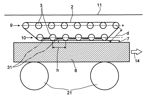
In the embodiment represented in Figure 7, an electrically conductive
structure 7
on a substrate 8 is coated with a device designed according to the invention.
The
device comprises a band 2, which is guided around a plurality of shafts 3. The
shafts 3 are arranged in an upper row 9 and a lower row 10. The shafts of the
lower row 10 are connected cathodically, while the shafts of the upper row 9
are
connected anodically. The voltage of the cathodically connected shafts of the
lower row 10 is transmitted to the electrically conductive structure 7 via the
band
2. By means of this, the electrically conductive structure 7 is likewise
charged
negatively so that metal ions of the electrolyte solution, in which the
substrate 8
PF 0000057900/HMS CA 02649786 2008-10-17
-20-
and the device are held, deposit to form a metal layer. Since the shafts 3 of
the
lower row 10 and the band 2 in the region of the lower row 10 are negatively
charged, metal ions likewise deposit on them. So that the metal deposited on
the
band 2 can be removed again, the upper row 9 is connected anodically. By means
of this, the band 2 is charged positively in the region of the upper row 9 and
the
metal ions pass back into the electrolyte solution. The liquid level of the
bath of
electrolyte solution is denoted by reference numeral 11 and is represented by
a
solid line.
In addition to the anodically connected shafts of the upper row 9, anodes 31
may
be arranged between the cathodes as represented here. The anodes 31 are, for
example, designed as flat rods.
So that there is no short circuit in the band 2, the band 2 in the embodiment
represented in Figure 7 is constructed as represented in Figure 8. Here, the
band
2 comprises electrically conductive sections 12 and electrically nonconductive
sections, i.e. insulating sections 13. The length L of an electrically
conductive
section 12 is preferably greater than or equal to the distance h between two
cathodically connected shafts 3. In order to avoid a short circuit, however,
the
length L of an electrically conductive section 12 must be less than the
distance d
from a cathodically connected shaft to a neighboring anodically connected
shaft.
The transport direction of the substrate 8 is represented by the arrow 14. In
order
to press the substrate against the barid 2, pressure rolls 21 are arranged
below
the substrate 8. The substrate 8 is guided through between the pressure rolls
21
and the band 2. The required pressure force may be achieved on the one hand in
that the pressure rolls 21 are mountecl firmly and the shafts 3, around which
the
band 2 runs, are sprung-mounted and pressed against the substrate 8, or in
that
the shafts 3 are mounted firmly and the pressure rolls 21 are mounted a mobile
fashion and moved against the substrate 8 with the required pressure force.
When
it is intended that the shafts 3 of the upper row 9 and of the lower row 10
can
change their position, it is preferable for the pressure rolls 21 to be
mounted firmly
and for the required application pressui-e to be applied onto the substrate 8
by the
mobile shafts 3 of the lower row 10.
Instead of the individual pressure rolls 21 as represented in Figure 7, it is
also
possible to use a band which runs around shafts and which, for example, is
PF 0000057900/HMS CA 02649786 2008-10-17
-21-
constructed like the cathode represented in Figure 2 but without being
electrically
conductive.
In a further embodiment, another electrolytic coating device may be arranged
below the substrate 8 instead of the pressure rolls 21. In this case, the
substrate 8
can then be coated simultaneously on its upper side and its lower side.
Figure 9 shows a side view of a device designed according to the invention in
a
further embodiment.
In the embodiment represented in Figure 9, the shafts of the anodically
connected
upper row 9 are arranged offset with respect to the shafts of the cathodically
connected lower row 10. The distance h between two anodically connected
shafts,
or between two cathodically connected shafts, is selected respectively so that
an
anodically connected shaft can be guided through between two neighboring
cathodically connected shafts and a cathodically connected shaft between two
anodically connected shafts. The arrows 15 in Figure 9 represent the fact that
the
shafts of the lower row 10 can be raised and the shafts of the upper row 9 can
be
lowered. This makes it possible for the metal deposited on the cathodically
connected shafts to be removed even in continuous production operation. To
this
end, the cathodically connected shafts of the lower row 10 are raised as
represented by the arrows 15, while the shafts of the upper row 9 are lowered
as
represented by the arrows 16. At the same time, the polarity of the shafts is
reversed so that after lowering the upper row 9, these shafts are connected
cathodically, and after raising the lower row 10, these shafts are connected
anodically. Owing to the polarity change, metal now deposits on the shafts of
the
upper row 9 which were previously connected anodically but now form the lower
row 10 and are connected anodically, while metal is removed from the shafts of
the lower row 10 which were previously connected cathodically, so long as they
form the upper row 9 and are connected anodically.
Besides the embodiment as represented in Figures 3 and 5, in which all the
shafts
of the upper row 9 are connected anodically and all the shafts of the lower
row 10
are connected cathodically, it is also possible to provide at least one
transport
shaft which is electrically nonconductive in each row. Preferably, the
transport
shafts are respectively the first and/or last shaft of a row 9, 10.
PF 0000057900/HMS CA 02649786 2008-10-17
-22-
So that all the metal can be removed again from the shafts 3 and the bands 2,
at
least as many shafts 3 are connected anodically as cathodically. The number of
the anodically connected shafts is preferably greater than that of the
cathodically
connected shafts. In order to achieve this, for example in the embodiment
represented in Figure 9, the first shaft of the upper row 9 always remains
connected anodically and stays in its position.
Figure 10 shows an electrolytic coating device in a further embodiment.
In the device represented in Figure 10, the substrate 8 is coated
simultaneously
on the upper and lower sides. To this end, the substrate 8 is guided through
between an upper device 17 and a lower device 18. The distance between the
upper device 17 and the lower device 18 is selected so that it corresponds
precisely to the thickness of the substrate 8.
In the embodiment represented here, the shafts 19 next to the substrate are
respectively connected cathodically, while the shafts 20 remote from the
substrate
are connected anodically. In the embodiment represented in Figure 10 ~as well,
the
shafts 19 can preferably be raised from the substrate 8 and the shafts 20
lowered
onto the substrate 8. The polarity of the shafts is simultaneously reversed,
so that
the shafts 20 are connected cathodically as soon as they contact the substrate
8,
and the shafts 19 are connected anodically as soon as they are raised from the
substrate 8. In the embodiment represented here, a plurality of bands 2 are
arranged in series on the upper side and the lower side of the substrate 8.
The
bands 2 are respectively guided around separate shafts. The successively
arranged bands 2 are preferably arranged mutually offset.
The embodiment represented in Figure 11 corresponds substantially to the
embodiment represented in Figure 10. However, a cathodically connected shaft
19 and an anodically connected shaft 20 respectively form the rear shaft of a
band
2 and simultaneously the front shaft of a further band 22, which is
represented
here by dashes. In plan view, the arrangement of the bands 2 and of the
further
bands 22 represented by dashes corresponds to the arrangement represented in
Figure 1. Here, the bands 22 are respectively arranged offset behind the bands
2.
Figure 12 represents an enlarged representation of a first embodiment of a
band
designed according to the invention with electrically conductive sections and
CA 02649786 2008-10-17
PF 0000057900/HMS
-23-
electricafly nonconductive sections.
The band 2 schematically represented here is constructed from individual
conductive segments 23 and nonconductive segments 24. The individual
segments 23, 24 are respectively fastened to one another by brackets 25. The
length of the conductive sections is established by the number of conductive
segments 23 which are fastened together. An electrically nonconductive section
is
in each case arranged between two conductive sections. In general, it is
sufficient
merely to use a single electrically noriconductive segment 24 for the
electrically
nonconductive section. It is nevertheless also possible to arrange a plurality
of
nonconductive segments 24 in series.
Figure 13 represents a further embodiment of a band 2. The band 2 is made from
a flexible support 26, around which an electrically conductive wire 27 is
wound in
order to produce an electrically conductive section 12. A suitable flexible
support
26 is, for example, a nonconductive plastic band which is optionally made of
an
elastomer. Instead of the electrically conductive wire 27 represented in
Figure 13,
for example, an electrically conductive foil may be wound around the flexible
support 26 in order to produce the electrically conductive section 12.
A further embodiment of a band 2 is schematically represented in a plan view
in
Figure 14 and a side view in Figure 15. The band 2 represented here comprises
two flexible nonconductive supports 26, on which conductive sections 32 are
fastened at a regular spacing. The conductive sections 32 may, for example, be
fastened on the conductive supports 26 by adhesive bonding. The conductive
sections 32 may be either rigid or flexible. In the case of rigid conductive
sections
32, their width is preferably selected so that they can run around the shafts
3. To
this end, it is necessary for the width of the conductive sections 32 to be
less than
the radius of the shaft 3. If the conductive sections 32 are intended to be
made
wider, they are preferably made of this flexible material. A suitable material
is, for
example, a likewise flexible metal foil. The nonconductive support 26 and/or
the
conductive sections 32 of the band 2 may also be provided with holes or
designed
in the form of a network.
Besides the embodiments of the bands 2 with electrically conductive sections
12
and electrically nonconductive sections 13 as represented in Figures 12 to 15,
any
other structure known to the person skilled in the art from which a band,
which
PF 0000057900/HMS CA 02649786 2008-10-17
-24-
alternately has electrically conductive and electrically nonconductive
sections, can
be produced is possible. For example, it is possible to provide a network
structure
as the band 2, an electrically conductive network being connected to an
electrically nonconductive network, wire or polymer support in order to form
the
electrically conductive sections 12 and electrically nonconductive sections
13. For
example, the electrically conductive sections in the form of a network may
then be
connected to the meshes of a nonconductive section with the aid of a wire
which
is guided through the individual meshes of the network structure.
Figure 16 shows an embodiment of a device designed according to the invention,
in which the shafts 3 are constructed from individual conductive segments 35
and
nonconductive segments 36. The conductive segments 35 and the nonconductive
segments 36 are arranged alternately. This makes it possible for a conductive
segment 35 to be connected cathodically and for a neighboring conductive
segment 35, which is separated from the cathodically connected segment 35 by a
nonconductive segment 36, to be connected anodically. In order to prevent a
short
circuit, it is necessary for the band 2 running around the shafts 3 to be
configured
with individual conductive 12 and electrically nonconductive sections 13. The
nonconductive sections 13 of the band 2 must be arranged so that they
respectively rest on a nonconductive segment 36 of the shaft. Removal of the
metal deposited on the cathodically connected segment 35 of the shaft and the
cathodically connected section 12 of the band 2 is achieved by connecting them
anodically in a further revolution. To this end, sliding contacts 37, 38 are
preferably provided on the shafts 3. The first sliding contact 37 is used as
an
anode, and the second sliding contact 38 as a cathode. So long as a conductive
segment 35 is in contact with the first sliding contact 37, this segment 35 is
connected anodically, and it is connected cathodically as soon as it comes in
contact with the second sliding contact 38. Besides the sliding contacts 37,
38
described here, it is also possible to use any other contact which does not
hinder
rotation of the shafts 3, and with which the conductive segments 35 can be
selectively connected cathodically and anodically. The distance between the
anode 37 and the cathode 38 must be large enough to prevent simultaneous
contact of the anode 37 and cathode 38 with a conductive segment 35.
Owing to the anodically connected electrically conductive segments 35, in the
embodiment represented in Figure 16 it is not necessary to provide further
additional anodes. It is nevertheless possible to arrange further anodes
between
PF 0000057900/HMS CA 02649786 2008-10-17
-25-
the shafts 3, for example in the form of flat rods.
Figure 17 shows a side view of anodes during the electrolytic coating.
Figure 18 shows the anodes in a position when the shafts 3 (which are not
represented here) change their position.
If anodes 31 are provided in addition to the anodically connected shafts 3 or
electrically conductive segments of the shafts 3, they may for example be
constructed as represented in Figures 17 and 18.
During the coating process, the anocles 31 are in their deployed position. For
a
substrate 8 which is coated simultaneously on the upper side and the lower
side,
they are then arranged above and below the substrate 8. When only one side of
the substrate 8 is coated, the anode 31 is preferably arranged on the side of
the
substrate 8 which is coated. In this case, care should be taken that the anode
31
does not touch the substrate. Otherwise, on the one hand, a short circuit
could
occur when the cathode touches the same electrically conductive structure as
the
anode, and on the other hand metal previously deposited on the structure would
be removed again during the contact with the anode 31.
In order to make it possible to change the shafts, the anodes 31 can be moved
parallel to the surface of the substrate 8 which is to be coated, as
represented by
the double arrow 41 in Figure 18. The movement takes place transversely to the
direction in which the substrate is transported through the bath. This makes
it
possible to remove the anodes while the shafts 3 change their position. Damage
of the anodes 31 and shafts 3 is thereby avoided. In the embodiment
represented
here, the anodes 31 are made of a flexible material. This makes it possible
for the
anodes to be wound in respectively allocated anode winding/unwinding devices
40 and unwound therefrom. The anode winding/unwinding devices 40 are
preferably arranged above and below the bath, as represented here. Such
windable and unwindable anodes are, for example, made in the form of flexible
metal bands or resilient spirals. If the anodes made of resilient spirals, a
plurality
of the spirals are preferably fastened next to one another.
PF 0000057900/HMS CA 02649786 2008-10-17
-26-
List of References
1 cathode
2 band
3 shaft
4 gap
5 upper side
6 lower side
7 electrically conductive structure
8 substrate
9 upper row
10 lower row
11 liquid level
12 electrically conductive section
13 electrically nonconductive section
14 transport direction
15 movement direction of the shafts
16 movement direction of the shafts
17 upper device
18 lower device
19 cathodically connected shafts
20 anodically connected shafts
21 pressure roll
22 further band
23 conductive segment
24 nonconductive segment
25 bracket
26 flexible support
27 wire
groove
30 31 anode
32 conductive section
conductive segment
36 nonconductive segment
37 anode
35 38 cathode
anode winding/unwinding device
41 movement direction of the anode
PF 0000057900/HMS CA 02649786 2008-10-17
..27-
d distance between a cathodically connected shaft and an anodically connected
shaft
h distance between two cathodically connected shafts
L length