Note: Descriptions are shown in the official language in which they were submitted.
CA 02650475 2008-10-24
WO 2007/130017 PCT/US2006/016439
BUS LOOP POWER INTERFACE AND METHOD
Background of the Invention
1. Field of the Invention
The present invention relates to a bus loop power interface, and more
particularly, to a bus loop power interface and method for an instrumentation
bus.
2. Statement of the Problem
Flowmeters are used to measure the mass flow rate, density, and other
characteristics of flowing materials. The flowing materials can comprise
liquids,
gases, combined liquids and gases, solids suspended in liquids, and liquids
including gases and suspended solids. For example, flowmeters are widely used
in
the well production and refining of petroleum and petroleum products. A
flowmeter
can be used to determine well production by measuring a flow rate (i.e., by
measuring a mass flow through the flowmeter), and can even be used to
determine
the relative proportions of the gas and liquid components of a flow.
In many process control or industrial automation settings, a bus loop (or
instrumentation bus) is used to connect to various devices, such as sensor
devices
and other instrument devices. The bus loop is commonly used to deliver
electrical
power to the various attached instrument or sensor devices. In addition, the
bus
loop is also commonly used to communicate data both to and from the sensor or
instrument device. Therefore, the bus loop is connected to a master device
that
can provide regulated electrical power over the bus and that can perform
communications over the bus. The master device can send commands and/or
programming, data, calibrations and other settings, etc., to the sensor and
instrument devices. The master device can also receive data from the sensor
and
instrument devices, including identification data, calibration data,
measurement
data, operational data, etc.
FIG. I shows a two-wire bus loop 1 according to the prior art. The bus loop
1 can include a master device 2 that operates the bus loop 1, multiple sensor
or
instrument devices 3-5, and terminators 6. The master device 2 can pass
digital
communication signals to external devices, such as to monitoring and control
stations, for example. The master device 2 is connected to an electrical power
1
CA 02650475 2008-10-24
WO 2007/130017 PCT/US2006/016439
source and provides electrical power over the two-wire bus loop 1. The master
device 2 typically provides electrical power that is current limited, voltage
limited,
and power limited.
The bus loop 1 can comprise a FIELDBUS bus loop, for example. The term
FIELDBUS refers to a two-wire instrumentation bus standard that is typically
used
to connect together multiple instruments and is further capable of being used
to
provide digital communications between instruments. Alternatively, the bus
loop 1
can comprise other buses, such as PROFIBUS, HART, a 4-20 mA bus loop, etc.
FIG. 2 shows a prior art power regulation scheme for a prior art bus device 3
connected to the bus loop 1. The prior art bus device 3 includes voltage
regulator 8
and a load 9 in series with the voltage regulator S. The voltage regulator 8
maintains a constant voltage level to the load 9.
However, this prior art power regulation has drawbacks. The maximum
electrical power (P) provided in this prior art arrangement comprises the
output
voltage of the series regulator (V) multiplied by the loop current (I). A Ioop
interface
that uses this kind of linear regulation has poor power transfer because the
voltage
parameter V in the available power equation (P = V X I) is essentially fixed.
In
addition, the bus voltage dips when the loop current increases, due to the
relatively
high loop impedance.
One possible solution could be the use of a switch mode power supply
(SMPS). A SMPS is also referred to as a switched mode power supply or a
switching power supply. A SMPS generates a time varying signal from the DC bus
voltage, performs a voltage step-up conversion, and converts the resulting
time-
varying signal back to a DC voltage that can have a higher voltage level than
the
original DC bus voltage. As a result, the V term in the power equation can be
increased.
However, the drawback of a SMPS device is that a SMPS device typically
has a low input impedance characteristic. This is not compatible with a device
powered from the bus loop 1, where the loop impedance is kept high in order to
enable communication signals to pass over the bus loop 1.
Summary of the Solution
A bus loop power interface is provided according to an embodiment of the
invention. The bus loop power interface comprises a voltage control module
receiving a loop voltage VLoop and generating a predetermined supply voltage
2
CA 02650475 2008-10-24
WO 2007/130017 PCT/US2006/016439
VSUPPLY, an impedance control module coupled to the voltage control module,
with
the impedance control module receiving a loop current ILOOP and generating a
predetermined supply current IsuPPLY, and a feedback coupled between the
voltage
control module and the impedance control module. The feedback provides a
feedback signal to the voltage control module that enables the voltage control
module to substantially maintain the predetermined supply voltage VSUPPLY.
A bus loop power interface is provided according to an embodiment of the
invention. The bus loop power interface comprises a switch mode power supply
(SMPS) U2 receiving a loop voltage VLooP and generating a predetermined supply
voltage VSUPPLY. The bus loop power interface further comprises a current
measuring resistor R, receiving a loop current ILOOP, an op-amp U, including
input
terminals across the current measuring resistor RI, and a transistor Q, biased
by
the op-amp Ul. The transistor Q, receives the loop current ILooP and generates
a
predetermined supply current IsuPPLY. The output of the op-amp U, controls an
impedance characteristic of the transistor Q, and controls the predetermined
supply
current ISUPPLY= The bus loop power interface further comprises a transistor
Q2
coupled to the SMPS U2. The transistor Q2 is biased by the loop voltage VLOOP.
The bus loop power interface further comprises a feedback resistor R2
connected
between the transistor Q2 and ground. The feedback resistor R2 receives a
feedback current IF from the transistor Q2. A feedback voltage VFB across the
feedback resistor R2 is received by a feedback input FB of the SMPS U2. The
transistor Q2 and the feedback resistor R2 enable the SMPS U2 to substantially
maintain the predetermined suppiy voltage VSUPPLY.
A method of controlling electrical power in a bus loop power interface is
provided according to an embodiment of the invention. The method comprises
receiving electrical power from an instrumentation bus at a loop voltage VLOOP
and
at a loop current ILOOP, generating a predetermined supply voltage VsuPPLY
from the
loop voltage VLOOP, and generating a predetermined supply current IsuPPLY,
with the
predetermined supply current IsuPPLY being related to a predetermined
impedance
characteristic of the bus loop power interface.
ASPECTS
In one aspect of the bus loop power interface, the predetermined supply
current IsuPPLY is substantially fixed.
3
CA 02650475 2008-10-24
WO 2007/130017 PCT/US2006/016439
In another aspect of the bus loop power interface, the predetermined supply
current IsuPPLY is varying. -
In yet another aspect of the bus loop power interface, the impedance control
module regulates electrical impedance in the bus loop power interface.
In yet another aspect of the bus loop power interface, the impedance control
module further comprises an impedance control line, with the impedance control
line being configured to control the predetermined supply current IsuPPLY and
control
an electrical impedance of the impedance control module.
In yet another aspect of the bus loop power interface, the bus loop power
interface further comprises a pair of input terminals and a pair of output
terminals,
wherein the impedance control module receives the loop current.l1-ooP from the
input terminals and wherein the voltage control module is connected to the
pair of
output terminals.
In yet another aspect of the bus loop power interface, the voltage control
module further comprises a switch mode power supply (SMPS) U2.
In yet another aspect of the bus loop power interface, the impedance control
module further comprises a current measuring resistor R, receiving the loop
current
ILOOP, an op-amp U, including input terminals across the current measuring
resistor
RI, and a transistor Q, biased by the op-amp U, and receiving the loop current
ILOOP, with the output of the op-amp U, controlling an impedance
characteristic of
the transistor Q, and controlling the predetermined supply current IsuppLy.
In yet another aspect of the bus loop power interface, the feedback
comprises a transistor Q2 that is biased by the-loop voltage VLOoP and a
feedback
resistor R2 connected between the transistor Q2 and ground, with the feedback
resistor R2 receiving a feedback current IF from the transistor Q2, wherein a
feedback voltage VFB across the feedback resistor R2 is received by a feedback
input FB of the SMPS U2.
'In yet another aspect of the bus loop power interface, the SMPS U2
comprises a voltage control module.
In yet another aspect of the bus loop power interface, the current measuring
resistor Rl, the op-amp Ul, and the transistor Q, comprise an impedance
control
module.
In yet another aspect of the bus loop power interface, the transistor Q2 and
the feedback resistor R2 comprise a feedback.
4
CA 02650475 2008-10-24
WO 2007/130017 PCT/US2006/016439
In yet another aspect of the bus loop power interface, the current measuring
resistor Rl, the op-amp Ul, and the transistor Q, regulate electrical
impedance in
the bus loop power interface.
In yet another aspect of the bus loop power interface, the bus loop power
interface further comprises an impedance control line configured to control
the
predetermined supply current IsuPPLY and control an electrical impedance of
the
impedance control module.
In yet another aspect of the bus loop power interface, the bus loop power
interface further comprises an impedance control line coupied to the op-amp
Ul,
with the impedance control line being configured to control a bias voltage of
the
transistor Ql.
In one aspect of the method, the method maximizes the electrical power
available to the bus loop power interface.
In another aspect of the method, the method maximizes the electrical power
available to the bus loop power interface while maintaining a substantially
high
impedance.
In yet another aspect of the method, the method maximizes the electrical
power available to the bus loop power interface by maximizing the
predetermined
supply voltage VsuPPLY and the predetermined supply current 1suPPLY.
In yet another aspect of the method, the method further comprises regulating
the predetermined supply current 1suPPLY to generate a communication signal.
In yet another aspect of the method, the method further comprises receiving
an impedance controi input and generating the predetermined supply current
1suPPLY based on the impedance control input.
In yet another aspect of the method, the bus loop power interface comprises
a voltage control module receiving a loop voltage VLoop and generating a
predetermined supply voltage VsuPPLY, an impedance control module coupled to
the
voltage control module, with the impedance control module receiving a loop
current
lLooP and generating, a predetermined supply current IsuPPLY, and a feedback
coupled between the voltage control module and the impedance control module,
with the feedback providing a feedback signal to the voltage control module
that
enables the voltage control module to substantially maintain the.
predetermined
supply voltage VSUPPLY.
5
CA 02650475 2008-10-24
WO 2007/130017 PCT/US2006/016439
In yet another aspect of the method, the predeterrrmined supply current
IsuPPLv is substantially fixed.
In yet another aspect of the method, the predetermined supply current
1suPPLY is varying.
In yet another aspect of the method, the impedance control module further
comprises an impedance control line, with the impedance control line being
configured to control the predetermined supply current IsuPPLY and control an
electrical impedance of the impedance control module.
In yet another aspect of the method, the voltage control module further
comprises a switch mode power supply (SMPS) U2.
In yet another aspect of the method, the impedance control module further
comprises a current measuring resistor R, receiving the loop current IlooP, an
op-
amp U, including input terminals across the current measuring resistor Ri, and
a
transistor Q, biased by the op-amp U, and receiving the loop current lLOOP,
with the
output of the op-amp U, controlling an impedance characteristic of the
transistor Q,
and controlling the predetermined supply current IsuPPLY=
In yet another aspect of the method, the feedback further comprises a
transistor Q2 that is biased by the loop voltage VLooP and a feedback resistor
R2
connected between the transistor Q2 and ground, with the feedback resistor R2
receiving a feedback current IF from the transistor Q2, wherein a feedback
voltage
VFB across the feedback resistor R2 is received by a feedback input FB of the
SMPS U2.
Description of the Drawings
FIG. I shows a two-wire bus loop according to the prior art.
FIG. 2 shows a prior art power regulation scheme'for a prior art bus device
connected to the bus loop.
FIG. 3 shows a bus loop power interface according to an embodiment of the
invention.
FIG. 4 shows the bus loop power interface according to an embodiment of
the invention.
Detailed Description of the Invention
FIGS. 3-4 and the following description depict specific examples to teach
those skilled in the art how to make and use the best mode of the invention.
For
6
CA 02650475 2008-10-24
WO 2007/130017 PCT/US2006/016439
the purpose of teaching inventive principles, some conventional aspects have
been
simplified or omitted. Those skilled in the art will appreciate variations
from these
examples that fall within the scope of the invention. Those skilled in the art
will
appreciate that the features described below can be combined in various ways
to
form multiple variations of the invention. As a result, the invention is not
limited to
the specific examples described below, but only by the claims and their
equivalents.
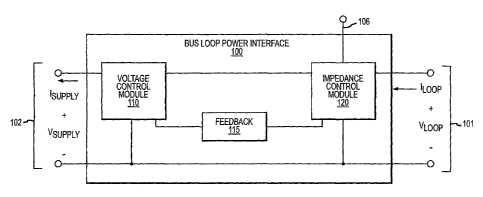
FIG. 3 shows a bus loop power interface 100 according to an embodiment of
the invention. The bus loop power interface 100 provides electrical power to a
bus
device attached to an instrument bus loop 1(not shown). The bus loop power
interface.100 can be the only device attached to the bus loop 1 or can be one
bus
instrument of many.
The bus device in one embodiment comprises a flow meter, such as a
Coriolis flow meter or a vibrating densitometer, for example. However, other
bus
devices are contemplated and are within the scope of the description and
claims.
The bus loop power interface 100 includes a voltage control module 110, an
impedance control module 120, and a feedback 115 coupled between the voltage
control module 110 and the impedance control module 120. The bus loop power
interface 100 includes a pair of input terminals 101 configured to be coupled
to an
bus loop 1 and a pair of output terminals 102 configured to be coupled to a
sensor
or instrument device (also not shown). The impedance control module 120
receives the loop current ILooP from the input terminals 101 and the voltage
control
module 110 is connected to the pair of output terminals, 102. The bus loop
power
interface 100 receives a loop voltage VLOOP from the bus and provides a
predetermined supply voltage VSupPLY at the output terminals 102. In addition,
the
bus loop power interface 100 receives a loop current ILOOP from the bus and
provides a predetermined supply current IsuPPLY at the output terminals 102.
The voltage control module 110 provides the predetermined supply voltage
VSUPPLY from the loop voltage VLooP. The voltage control module 110 includes a
switch mode power supply (SMPS) in some embodiments. The supply voltage
VSUPPLY of the voltage control moduie 110 (and of the bus loop power interface
100)
can comprise a direct current (DC) voltage in some embodiments. Alternatively,
the suppiy voltage VsuPPLY can comprise a DC voltage including a superimposed
digital communication signal.
7
CA 02650475 2008-10-24
WO 2007/130017 PCT/US2006/016439
The supply voltage VsuppLy can be less than the loop voltage VLOOP. The
supply voltage VsuppLy can be greater than or equal to the loop voltage VLOOP.
The
supply voltage VSUPPLY can be at a fixed or varying level.
The impedance control module 120 regulates electrical impedance in the
bus loop power interface 100. The impedance .control module 120 provides the
predetermined supply current IsupPLY from the loop current ILooP. The supply
current IsuPPLY is generated by varying the impedance provided by the
impedance
control module 120. As a result, the impedance of the bus loop power interface
100 can be maintained at a relatively high impedance level.
In some embodiments, the predetermined supply current IsuPPLY produced
by the impedance control module 120 is substantially fixed. Alternatively, in
other
embodiments the predetermined supply current IsuPPLY is varying, such as in
embodiments where a varying current is used to generate a communication
signal.
In some embodiments, the impedance control module 120 includes an
impedance control line 106. The impedance control line 106 is configured to
control the predetermined supply current lsuPPLy and control the electrical
impedance of the impedance control module 120.
The impedance control line 106 can be used in some embodiments to vary
the supply current IsuPPLY, such as in embodiments that employ electrical
current to
generate a communication signal. Alternatively, in other embodiments the
impedance control line 106 can comprise a fixed value that generates a
substantially fixed impedance value (and therefore a substantially fixed
supply
current ISUPPLY).
The feedback 115 generates feedback from the impedance control module
120 to the voltage control module 110. The feedback 115 provides a feedback
signal to the voltage control module 110 that enables the voltage control
module
110 to substantially maintain the predetermined supply voltage VsuPPLY. The
feedback 115 can include a voltage level feedback, for example, wherein the
voltage control module 110 uses the voltage level feedback in order to
maintain the
supply voltage VsuPPLY. In addition or alternatively, the feedback 115 can
transfer
an error current to the voltage control module 110, wherein the error current
generates a feedback voltage that is used by the voltage control module 110 to
maintain the supply voltage VsuppLy (see FIG. 4 and the accompanying text).
8
CA 02650475 2008-10-24
WO 2007/130017 PCT/US2006/016439
The feedback 115 is used to generate and maintain the regulated supply
voltage VsuPPLY. In addition, the feedback 115 is also used to maximize
electrical
power output by the bus loop power interface 100 and therefore to achieve a
maximum power transfer. The feedback 115 can ensure that the bus loop power
interface 100 tracks a specific electrical power operating point. Even when
the
supply voltage VSUPPLY changes, the bus loop power interface 100 maximizes
available power. A bus device coupled to the pair of input terminals 101 may
have
to operate at a specific supply current IsupPLr that is determined by a
process value.
In such a case, the bus loop power interface 100 can still maximize the
available
power.
The bus loop power interface 100 can be used with any instrument bus, such
as a FIELDBUS, a PROFIBUS, or a HART bus, for example. In these applications,
a digital communication signal can be superimposed on the supplied electrical
power. Alternatively, the bus loop power interface 100 can be used for a 4-20
milliamp (mA) bus loop, for example, wherein the electrical current output is
modulated in order to generate a superimposed communication signal.
In some embodiments, the bus loop power interface 100 can be used in
intrinsically safe (IS) environments. An IS environment can include vapors,
gases,
liquids, dust, etc., that presents a fire or explosion hazard. Therefore, an
IS
compliant bus is limited in available current and/or voltage that it can
supply.
Advantageously, the bus loop power interface 100 can maximize delivered
electrical power by maximizing both the available voltage and the available
current.
This is achieved while maintaining a high input impedance. The bus loop power
interface 100 will substantially maintain the supply voltage VsuPPLY over
various
current levels. The bus loop power interface 100 therefore facilitates
communication while delivering maximum electrical power.
The bus loop power interface 100 implements a method of controlling
electrical power according to an embodiment of the invention. The bus loop
power
interface 100 receives electrical power from an instrumentation bus at a loop
'30 voltage VLooP and at a loop current ILooP, generates a predetermined
supply
voltage VsuPpLY from the loop voltage VLOOP, and generates a predetermined
supply
current IsuPPLY. The predetermined supply current IsuPPLY is related to a
predetermined impedance characteristic of the bus loop power interface.
9
CA 02650475 2008-10-24
WO 2007/130017 PCT/US2006/016439
The method maximizes the electrical power available to the bus loop power
interface 100. The method maximizes the electrical power available to the bus
loop
power interface 100 while maintaining a substantially high impedance. The
method
maximizes the electrical power available to the bus loop power interface 100
by
maximizing the predetermined supply voltage VsuPPLY and the predetermined
supply current IsuPPLY. This is achieved even where the supply voltage VSUPPLY
or
the supply current IsuPPLY may be constrained by a process value of the
corresponding bus device.
The method can regulate the predetermined supply current IsuPPLY in order
to generate a communication signal. The method can receive an impedance
control input and can generate the predetermined supply current IsuPPLY based
on
the impedance control input.
FIG. 4 shows the bus loop power interface 100 according to an embodiment
of the invention. The bus loop power interface 100 in this embodiment inciudes
the
voltage control module 110, the impedance control module 120, and the feedback
115, as previously discussed.
The voltage control module 110 in this embodiment includes a switch mode
power supply (SMPS) U2, an inductor LI, capacitors C, and C2, a diode Dl, and
a
Zener diode ZI. As previously discussed, the predetermined supply voltage
VsuPPLY
can comprise a DC voltage that is greater than, equal to, or less than the
loop DC
voltage VLooP. The capacitor, inductor, and diode components can be chosen to
achieve the predetermined supply voltage VsuPPLY=
The impedance control module 120 in this embodiment includes an op-amp
Ul, a resistor RI, a voltage input V_ISet, and a transistor Qti. The op-amp U,
includes input terminals across the resistor RI. The transistor Q, is biased
by the
op-amp Ul. The resistor R, receives the loop current ILooP and the transistor
Q,
receives the loop current ILooP and generates a predetermined supply current
IsuPPLY= The op-amp U, is configured to measure the voltage across the
resistor Rl,
wherein the voltage is generated by an electrical current (i.e., ILOOP)
flowing through
the resistor Rl. The.measured current is used to control the gate (G) voltage
of the
transistor Ql. Changing the voltage bias of the gate of the transistor Q,
changes
the source-to-drain impedance of the transistor Ql.
CA 02650475 2008-10-24
WO 2007/130017 PCT/US2006/016439
The voltage input V Iset in some embodiments comprises the impedance
control input 106 of FIG. 3. The impedance control line 106 is coupled to the
op-
amp U, and can therefore control a bias voltage of the transistor Ql.
The transistor Q, can comprise a power transistor. In the embodiment
shown, the transistor QT comprises a field effect transistor (FET) or a metal
oxide
semiconductor field effect transistor (MOSFET), such as a BSP 149 transistor,
available from Infineon Technologies AG. However, any suitable transistor
device
can be used, and is within the scope of the description and claims.
The feedback 115 in this embodiment includes a transistor Q2 and a
feedback resistor R2. The transistor Q2 is biased by the loop voltage VLOOP.
The
feedback resistor R2 is connected between the transistor Q2 and ground. The
feedback resistor R2 receives a feedback current IF from the transistor Q2. A
feedback voltage VFB across the feedback resistor R2 is received by a feedback
input FB of the SMPS U2. When the actual supply voltage VsuPPLY increases to
above a target supply voltage, the bias voltage at the base of the transistor
Q2 will
increase. If the voltage across the base-collector junction of the transistor
Q2 (i.e.,
VBC of Q2) becomes greater than' 0.7 volts, then a positive feedback current
IFB will
flow through the feedback resistor R2 to ground. This in turn causes the
voltage
across the feedback resistor R2 to increase and consequently places a higher
feedback voltage on the feedback (FB) pin of the SMPS U2. As a result, the
supply
voltage VsuPPLY will be reduced by the SMPS U2. Conversely, if the actual
supply
voltage VsuPPLY drops below the predetermined supply voltage, the feedback
voltage at the FB pin will decrease and the SMPS U2 will bring the actual
supply
voltage VsuPPLY up to substantially the same level as the predetermined target
supply voltage VSUPPLY. The transistor Q2 and the feedback resistor R2 enable
the
SMPS U2 to substantially maintain the predetermined supply voltage VsuPPLY=
The invention can advantageously maximize available power at the pair of
output terminals 102. The power can be represented as:
P = [VLOOP - (VBE Of Q2)] * ILOOP * (E of U2) (1)
where (VBE of Q2) is the voltage across the base-emitter junction of
transistor Q2
and where (E of U2) is the switching efficiency of the SMPS U2. The term
[VLOOP --
(VBE of Q2)] comprises the voltage Vc, across the capacitor Cl, and is
equivalent to
the supply voltage VSUPPLY.
11
CA 02650475 2008-10-24
WO 2007/130017 PCT/US2006/016439
In one embodiment, the transistor Q2 comprises a bipolar junction transistor
(BJT), such as a BC 859 transistor, available from Fairchild Semiconductor
Corporation. However, it should be understood that other transistors are
contemplated and are within the scope of the description and claims.
The bus loop power interface and method according to the invention can be
employed according to any of the embodiments in order to provide several
advantages, if desired. The invention provides a regulated electrical voltage.
The
invention provides a regulated electrical current. The invention provides a
high
input impedance. The invention provides an ability to control current. The
invention provides an ability to control impedance. The invention provides a
maximized electrical power.
12