Note: Descriptions are shown in the official language in which they were submitted.
CA 02650532 2008-10-24
WO 2007/133323 PCT/US2007/006197
1
Systems and Methods of RF Power Transmission, Modulation, and
Amplification
Background of the Invention
Field of the Invention
[00011 The present invention relates generally to RF power transmission,
modulation,
and amplification. More particularly, the invention relates to methods and
systems for
vector combining power amplification.
Background Art
[0002] In power amplifiers, a complex tradeoff typically exists between
linearity and
power efficiency.
100031 Linearity is determined by a power amplifier's operating range on a
characteristic curve that relates its input to output variables -- the more
linear the
operating range the more linear the power amplifier is said to be. Linearity
is a
desired characteristic of a power amplifier. In one aspect, for example, it is
desired
that a power amplifier uniformly amplifies signals of varying amplitude,
and/or phase
and/or frequency.. Accordingly, linearity is an important determiner of the
output
signal quality of a power amplifier.
[0004] Power efficiency can be calculated using the relationship of the total
power
delivered to a load divided by the total power supplied to the amplifier. For
an ideal
amplifier, power efficiency is 100%. Typically, power amplifiers are divided
into
classes which determine the amplifier's maximum theoretical power efficiency.
Power efficiency is clearly a desired characteristic of a power amplifier --
particularly,
in wireless communication systems where power consumption is significantly
dominated by the power amplifier.
[0005] Unfortunately, the traditional tradeoff between linearity and
efficiency in
power amplifiers is such that the more linear a power amplifier is the less
power
efficient it is. For example, the most linear amplifier is biased for class A
operation,
which is the least efficient class of amplifiers. On the other hand, higher
class
amplifiers such as class B,C,D,E, etc, are more power efficient, but are
considerably
non-linear which can result in spectrally distorted output signals.
[00061 The tradeoff described above is further accentuated by typical wireless
communication signals. Wireless communication signals, such as OFDM, CDMA,
and W-CDMA for example, are generally characterized by their peak-to-average
CA 02650532 2008-10-24
WO 2007/133323 PCT/US2007/006197
-2-
power ratios. The larger the signal's peak to average ratio the more non-
linear
distortion will be produced when non-linear amplifiers are employed.
[00071 Outphasing amplification techniques have been proposed for RF amplifier
designs. In several aspects, however, existing outphasing techniques are
deficient in
satisfying complex signal amplification requirements, particularly as defined
by
wireless communication standards, for example.
[0008] In one aspect, existing outphasing techniques employ an isolating
and/or a
combining element when combining constant envelope constituents of a desired
output signal. For example, it is commonly the case that a power combiner is
used to
combine the constituent signals. This combining approach, however, typically
results
in a degradation of output signal power due to insertion loss and limited
bandwidth,
and, correspondingly, a decrease in power efficiency.
[0009] In another aspect, the typically large size of combining elements
precludes
having them in monolithic amplifier designs.
[0010] What is needed therefore are power amplification methods and systems
that
solve the deficiencies of existing power amplifying techniques while
maximizing
power efficiency and minimizing non-linear distortion. Further, power
amplification
methods and systems that can be implemented without the limitations of
traditional
power combining circuitry and techniques are needed.
Brief Summary of the Invention
[0011] Embodiments for vector combining power amplification are disclosed
herein.
[0012] In one embodiment, a plurality of substantially constant envelope
signals are
individually amplified, then combined to form a desired time-varying complex
envelope signal. Phase and/or frequency characteristics of one or more of the
signals
are controlled to provide the desired phase, frequency, and/or amplitude
characteristics of the desired time-varying complex envelope signal.
[0013] In another embodiment, a time-varying complex envelope signal is
decomposed into a plurality of substantially constant envelope constituent
signals.
The constituent signals are amplified, and then re-combined to construct an
amplified
version of the original time-varying envelope signal.
CA 02650532 2008-10-24
WO 2007/133323 PCT/US2007/006197
-3-
[00141 Embodiments of the invention can be practiced with modulated carrier
signals
and with baseband information and clock signals. Embodiments of the invention
also
achieve frequency up-conversion. Accordingly, embodiments of the invention
represent integrated solutions for frequency up-conversion, amplification, and
modulation.
[0015] Embodiments of the invention can be implemented with analog and/or
digital
controls. The invention can be implemented with analog components or with a
combination of analog components and digital components. In the latter
embodiment,
digital signal processing can be implemented in an existing baseband processor
for
added cost savings.
[00161 Additional features and advantages of the invention will be set forth
in the
description that follows. Yet further features and advantages will be apparent
to a
person skilled in the art based on the description set forth herein or may be
learned by
practice of the invention. The advantages of the invention will be realized
and attained
by the structure and methods particularly pointed out in the written
description and
claims hereof as well as the appended drawings.
[00171 It is to be understood that both the foregoing summary and the
following
detailed description are exemplary and explanatory and are intended to provide
further explanation of embodiments of the invention as claimed.
Brief Description of the Figures
[0018] Embodiments of the present invention will be described with reference
to the
accompanying drawings, wherein generally like reference numbers indicate
identical
or functionally similar elements. Also, generally, the leftmost digit(s) of
the reference
numbers identify the drawings in which the associated elements are first
introduced.
[0019] FIG. 1 A is an example that illustrates the generation of an exemplary
time-
varying complex envelope signal.
[0020] FIG. 1B is another example that illustrates the generation of an
exemplary
time-varying complex envelope signal.
[0021] FIG. 1C is an example that illustrates the generation of an exemplary
time-
varying complex envelope signal from the sum of two or more constant envelope
signals.
CA 02650532 2008-10-24
WO 2007/133323 PCT/US2007/006197
-4-
[0022] FIG. 1 D illustrates the power amplification of an example time-varying
complex envelope signal according to an embodiment of the present invention.
[0023] FIG. 1E is a block diagram that illustrates a vector power
amplification
embodiment of the present invention.
[0024] FIG. 1 illustrates a phasor representation of a signal.
[0025] FIG. 2 illustrates a phasor representation of a time-varying complex
envelope
signal.
[0026] FIGs. 3A-3C illustrate an example modulation to generate a time-varying
complex envelope signal.
[0027] FIG. 3D is an example that illustrates constant envelope decomposition
of a
time-varying envelope signal.
[0028] FIG. 4 is a phasor diagram that illustrates a Cartesian 4-Branch Vector
Power
Amplification (VPA) method of an embodiment of the present invention.
[00291 FIG. 5 is a block diagram that illustrates an exemplary embodiment of
the
Cartesian 4-Branch VPA method.
[0030] FIG. 6 is a process flowchart embodiment for power amplification
according
to the Cartesian 4-Branch VPA method.
[0031] FIG. 7A is a block diagram that illustrates an exemplary embodiment of
a
vector power amplifier for implementing the Cartesian 4-Branch VPA method.
[0032] FIG. 7B is a block diagram that illustrates another exemplary
embodiment of a
vector power amplifier for implementing the Cartesian 4-Branch VPA method.
[0033] FIG. 8A is a block diagram that illustrates another exemplary
embodiment of a
vector power amplifier according to the Cartesian 4-Branch VPA method.
[0034] FIG. 8B is a block diagram that illustrates another exemplary
embodiment of a
vector power amplifier according to the Cartesian 4-Branch VPA method.
[0035] FIG. 8C is a block diagram that illustrates another exemplary
embodiment of a
vector power amplifier according to the Cartesian 4-Branch VPA method.
[0036] FIG. 8D is a block diagram that illustrates another exemplary
embodiment of a
vector power amplifier according to the Cartesian 4-Branch VPA method.
[0037] FIGs. 9A-9B are phasor diagrams that illustrate a Cartesian-Polar-
Cartesian-
Polar (CPCP) 2-Branch Vector Power Amplification (VPA) method of an
embodiment of the present invention.
CA 02650532 2008-10-24
WO 2007/133323 PCT/US2007/006197
-5-
[0038] FIG. 10 is a block diagram that illustrates an exemplary embodiment of
the
CPCP 2-Branch VPA method.
[0039] FIG. l0A is a block diagram that illustrates another exemplary
embodiment of
the CPCP 2-Branch VPA method.
[0040] FIG. 11 is a process flowchart embodiment for power amplification
according
to the CPCP 2-Branch VPA method.
[0041] FIG. 12 is a block diagram that illustrates an exemplary embodiment of
a
vector power amplifier for implementing the CPCP 2-Branch VPA method.
[0042] FIG. 12A is a block diagram that illustrates another exemplary
embodiment of
a vector power amplifier for implementing the CPCP 2-Branch VPA method.
[0043] FIG. 12B is a block diagram that illustrates another exemplary
embodiment of
a vector power amplifier for implementing the CPCP 2-Branch VPA method.
[0044] FIG. 13 is a block diagram that illustrates another exemplary
embodiment of a
vector power amplifier for implementing the CPCP 2-Branch VPA method.
[0045] FIG. 13A is a block diagram that illustrates another exemplary
embodiment of
a vector power amplifier for implementing the CPCP 2-Branch VPA method.
[0046] FIG. 14 is a phasor diagram that illustrates a Direct Cartesian 2-
Branch Vector
Power Amplification (VPA) method of an embodiment of the present invention.
[0047] FIG. 15 is a block diagram that illustrates an exemplary embodiment of
the
Direct Cartesian 2-Branch VPA method.
[0048] FIG. 15A is a block diagram that illustrates another exemplary
embodiment of
the Direct Cartesian 2-Branch VPA method.
[0049] FIG. 16 is a process flowchart embodiment for power amplification
according
to the Direct Cartesian 2-Branch VPA method.
[0050] FIG. 17 is a block diagram that illustrates an exemplary embodiment of
a
vector power amplifier for implementing the Direct Cartesian 2-Branch VPA
method.
[0051] FIG. 17A is a block diagram that illustrates another exemplary
embodiment of
a vector power amplifier for implementing the Direct Cartesian 2-Branch VPA
method.
[0052] FIG. 17B is a block diagram that illustrates another exemplary
embodiment of
a vector power amplifier for implementing the Direct Cartesian 2-Branch VPA
method.
CA 02650532 2008-10-24
WO 2007/133323 PCT/US2007/006197
-6-
[0053] FIG. 18 is a block diagram that illustrates another exemplary
embodiment of a
vector power amplifier for implementing the Direct Cartesian 2-Branch VPA
method.
[0054] FIG. 18A is a block diagram that illustrates another exemplary
embodiment of
a vector power amplifier for implementing the Direct Cartesian 2-Branch VPA
method.
[0055] FIG. 19 is a'process flowchart that illustrates an I and Q transfer
function
embodiment according to the Cartesian 4-Branch VPA method.
[0056] FIG. 20 is a block diagram that illustrates an exemplary embodiment of
an I
and Q transfer function according to the Cartesian 4-Branch VPA method.
[0057] FIG. 21 is a process flowchart that illustrates an I and Q transfer
function
embodiment according to the CPCP 2-Branch VPA method.
[00581 FIG. 22 is a block diagram that illustrates an exemplary embodiment of
an I
and Q transfer function according to the CPCP 2-Branch VPA method.
[0059] FIG. 23 is a process flowchart that illustrates an I and Q transfer
function
embodiment according to the Direct Cartesian 2-Branch VPA method.
[0060] FIG. 24 is a block diagram that illustrates an exemplary embodiment of
an I
and Q transfer function according to the Direct Cartesian 2-Branch VPA method.
[0061] FIG. 25 is a phasor diagram that illustrates the effect of waveform
distortion
on a representation of a signal phasor.
[0062] FIG. 26 illustrates magnitude to phase transform functions according to
an
embodiment of the present invention.
[0063] FIG. 27 illustrates exemplary embodiments of biasing circuitry
according to
embodiments of the present invention..
[0064] FIG. 28 illustrates a method of combining constant envelope signals
according
to an embodiment the present invention.
[0065] FIG. 29 illustrates a vector power amplifier output stage embodiment
according to the present invention.
[0066] FIG. 30 is a block diagram of a power amplifier (PA) output stage
embodiment.
[0067] FIG. 31 is a block diagram of another power amplifier (PA) output stage
embodiment.
CA 02650532 2008-10-24
WO 2007/133323 PCT/US2007/006197
-7-
[0068] FIG. 32 is a block diagram of another power amplifier (PA) output stage
embodiment.
[0069] FIG. 33 is a block diagram of another power amplifier (PA) output stage
embodiment according to the present invention.
[0070] FIG. 34 is a block diagram of another power amplifier (PA) output stage
embodiment according to the present invention.
[0071] FIG. 35 is a block diagram of another power amplifier (PA) output stage
embodiment according to the present invention.
[0072] FIG. 36 is a block diagram of another power amplifier (PA) output stage
embodiment according to the present invention.
[0073] FIG. 37 illustrates an example output signal according to an embodiment
of
the present invention.
[0074] FIG. 38 illustrates an exemplary PA embodiment.
[0075] FIG. 39 illustrates an example time-varying complex envelope PA output
signal and a corresponding envelop signal.
[0076] FIG. 40 illustrates example timing diagrams of a PA output stage
current.
[0077] FIG. 41 illustrates exemplary output stage current control functions.
[0078] FIG. 42 is a block diagram of another power amplifier (PA) output stage
embodiment.
[0079] FIG. 43 illustrates an exemplary PA stage embodiment.
[0080] FIG. 44 illustrates an exemplary waved-shaped PA output signal.
[0081] FIG. 45 illustrates a power control method.
[0082] FIG. 46 illustrates another power control method.
[0083] FIG. 47 illustrates an exemplary vector power amplifier embodiment.
[0084] FIG. 48 is a process flowchart for implementing output stage current
shaping
according to an embodiment of the present invention.
[0085] FIG. 49 is a process flowchart for implementing harmonic control
according to
an embodiment of the present invention.
[0086] FIG. 50 is a process flowchart for power amplification according to an
embodiment of the present invention.
[0087] FIGs. 51A-I. illustrate exemplary multiple-input single-output (MISO)
output
stage embodiments.
CA 02650532 2008-10-24
WO 2007/133323 PCT/US2007/006197
-8-
[0088] FIG. 52 illustrates an exemplary MISO amplifiier embodiment.
[0089] FIG. 53 illustrates frequency band allocation on lower and upper
spectrum
bands for various communication standards.
[0090] FIGs. 54A-B illustrate feedforward techniques for compensating for
errors.
[0091] FIG. 55 illustrates a receiver-based feedback error correction
technique.
[0092] FIG. 56 illustrates a digital control module embodiment.
[0093] FIG. 57 illustrates another digital control module embodiment.
[0094] FIG. 58 illustrates another digital control module embodiment.
[0095] FIG. 59 illustrates a VPA analog core embodiment.
[0096] FIG. 60 illustrates an output stage embodiment according to the VPA
analog
core embodiment of FIG. 60.
[0097] FIG. 61 illustrates another VPA analog core embodiment.
[0098] FIG. 62 illustrates an output stage embodiment according to the VPA
analog
core embodiment of FIG. 61.
[0099] FIG. 63 illustrates another VPA analog core embodiment.
[00100] FIG. 64 illustrates an output stage embodiment according to the VPA
analog
core embodiment of FIG. 63.
[00101] FIG. 65 illustrates real-time amplifier class control using an
exemplary
waveform, according to an embodiment of the present invention.
[00102] FIG. 66 is an example plot of output power versus outphasing angle.
[00103] FIG. 67 illustrates exemplary power control mechanisms using an
exemplary
QPSK waveform, according to an embodiment of the present invention.
[00104] FIG. 68 illustrates real-time amplifier class control using an
exemplary
waveform, according to an embodiment of the present invention.
[00105] FIG. 69 illustrates real-time amplifier class control using an
exemplary
waveform, according to an embodiment of the present invention.
[00106] FIG. 70 illustrates an exemplary plot of VPA output stage theoretical
efficiency versus VPA output stage current, according to an embodiment of the
present invention.
[00107] FIG. 71 illustrates an exemplary VPA according to an embodiment of the
present invention.
CA 02650532 2008-10-24
WO 2007/133323 PCT/US2007/006197
-9-
[00108] FIG. 72 is a process flowchart that illustrates a method for real-time
amplifier
class control in a power amplifier, according to an embodiment of the present
invention.
[00109] FIG. 73 illustrates an example VPA output stage.
[00110] FIG. 74 illustrates an equivalent circuit for amplifier class S
operation of the
VPA output stage of FIG. 73.
[00111] FIG. 75 illustrates an equivalent circuit for amplifier class A
operation of the
VPA output stage of FIG. 73.
[00112] FIG. 76 is a plot that illustrates exemplary magnitude to phase shift
transform
functions for amplifier class A and class S operation of the VPA output stage
of FIG.
73.
[00113] FIG. 77 is a plot that illustrates a spectrum of magnitude to phase
shift
transform functions corresponding to a range of amplifier classes of operation
of the
VPA output stage of FIG. 73.
[00114] FIG. 78 illustrates a mathematical derivation of the magnitude to
phase shift
transform in the presence of branch phase and amplitude errors.
[00115] The present invention will be described with reference to the
accompanying
drawings. The drawing in which an element first appears is typically indicated
by the
leftmost digit(s) in the corresponding reference number.
Detailed Description of the Invention
Table of Contents
1. Introduction
1.1. Example Generation of Time-Varying Complex Envelope Input Signals
1.2. Example Generation of Time-Varying Complex Envelope Signals from
Constant Envelope Signals
1.3. Vector Power Amplification Overview
2. General Mathematical Overview
CA 02650532 2008-10-24
WO 2007/133323 PCT/US2007/006197
-10-
2.1. Phasor Signal Representation
2.2. Time-Varying Complex Envelope Signals
2.3. Constant Envelope Decomposition of Time-Varying Envelope Signals
3. Vector Power Amplification (VPA) Methods and Systems
3.1. Cartesian 4-Branch Vector Power Amplifier
3.2. Cartesian-Polar-Cartesian-Polar (CPCP) 2-Branch Vector Power Amplifier
3.3. Direct Cartesian 2-Branch Vector Power Amplifier
3.4. I and Q Data to Vector Modulator Transfer Functions
3.4.1. Cartesian 4-Branch VPA Transfer Function
3.4.2. CPCP 2-Branch VPA Transfer Function
3.4.3. Direct Cartesian 2-Branch VPA Transfer Function
3.4.4. Magnitude to Phase Shift Transform
3.4.4.1. Magnitude to Phase Shift Transform for Sinusoidal
Signals
3.4.4.2. Magnitude to Phase Shift Transform for Square Wave
Signals
3.4.5. Waveform Distortion Compensation
3.5. Output Stage
3.5.1. Output Stage Embodiments
3.5.2. Output Stage Current Shaping
3.5.3. Output Stage Protection
3.6. Harmonic Control
3.7. Power Control
3.8. Exemplary Vector Power Amplifier Embodiment
4. Additional Exemplary Embodiments and Implementations
4.1.. Overview
CA 02650532 2008-10-24
WO 2007/133323 PCT/US2007/006197
-11-
4.1.1. Control of Output Power and Power Efficiency
4.1.2. Error Compensation and/or Correction
4.1.3. Multi-Band Multi-Mode Operation
4.2. Digital Control Module
4.3. VPA Analog Core
4.3.1. VPA Analog Core Implementation A
4.3.2. VPA Analog Core Implementation B
4.3.3. VPA Analog Core Implementation C
5. Real-Time Amplifier Class Control of VPA Output Stage
6. Summary
7. Conclusions
CA 02650532 2008-10-24
WO 2007/133323 PCT/US2007/006197
-12-
Introduction
[00116] Methods, apparatuses and systems for vector combining power
amplification
are disclosed herein.
[00117] Vector combining power amplification is an approach for optimizing
linearity
and power efficiency simultaneously. Generally speaking, and referring to
flowchart
502 in FIG. 50, in step 504 a time-varying complex envelope input signal, with
varying amplitude and phase, is decomposed into constant envelope constituent
signals. In step 506, the constant envelope constituent signals are amplified,
and then
in step 508 summed to generate an amplified version of the input complex
envelope
signal. Since substantially constant envelope signals may be amplified with
minimal
concern for non-linear distortion, the result of summing the constant envelope
signals
suffers minimal non-linear distortion while providing optimum efficiency.
[00118] Accordingly, vector combining power amplification allows for non-
linear
power amplifiers to be used to efficiently amplify complex signals whilst
maintaining
minimal non-linear distortion levels.
[00119] For purposes of convenience, and not limitation, methods and systems
of the
present invention are sometimes referred to herein as vector power
amplification
(VPA) methods and systems.
[00120] A high-level description of VPA methods and systems according to
embodiments of the present invention is now provided. For the purpose of
clarity,
certain terms are first defined below. The definitions described in this
section are
provided for convenience purposes only, and are not limiting. The meaning of
these
terms will be apparent to persons skilled in the art(s) based on the entirety
of the
teachings provided herein. . These terms may be discussed throughout the
specification with additional detail.
[00121] The term signal envelope, when used herein, refers to an amplitude
boundary
within which a signal is contained as it fluctuates in the time domain.
Quadrature-
modulated signals can be described by r(t) = i(t)=cos(ooc=t) + q(t)=sin((oc=t)
where i(t) and
q(t) represent in-phase and quadrature signals with the signal envelope e(t),
being
equal to e(t) = Ji(t)Z + q(t)2 and the phase angle associated with r(t) is
related to arctan
(q(t)/i(t).
CA 02650532 2008-10-24
WO 2007/133323 PCT/US2007/006197
-13-
[00122] The term constant envelope signal, when used herein, refers to in-
phase and
quadrature signals where e(t) = i(t)2 + q(t)2, with e(t) having a relatively
or
substantially constant value.
[00123] The term time-varying envelope signal, when used herein, refers to a
signal
having a time-varying signal envelope. A time-varying envelope signal can be
described in terms of in-phase and quadrature signals as e(t) = Ji(t)2 +
q(t)2,with e(t)
having a time-varying value.
[00124] The term phase shifting, when used herein, refers to delaying or
advancing the
phase component of a time-varying or constant envelope signal relative to a
reference
phase.
1.l) Example Generation of Complex Envelope Time- Varying Input Signals
[00125] FIGs. IA and 1B are examples that illustrate the generation of time-
varying
envelope and phase complex input signals. In FIG. lA, time-varying envelope
carrier
signals 104 and 106 are input into phase controller 110. Phase controller 110
manipulates the phase components of signals 104 and 106. In other words, phase
controller 110 may phase shift signals 104 and 106. Resulting signals 108 and
112,
accordingly, may be phased shifted relative to signals 104 and 106. In the
example of
FIG. lA, phase controller 110 causes a phase reversal (180 degree phase shift)
in
signals 104 and 106 at time instant to, as can be seen from signals 108 and
112.
Signals 108 and 112 represent time-varying complex carrier signals. Signals
108 and
112 have both time-varying envelopes and phase components. When summed,
signals 108 and 112 result in signal 114. Signal 114 also represents a time-
varying
complex signal. Signal 114 may be an example input signal into VPA embodiments
of the present invention (for example, an example input into step 504 of FIG.
50).
1001261 Time-varying complex signals may also be generated as illustrated in
FIG. 1B.
In FIG. 1B, signals 116 and 118 represent baseband signals. For example,
signals 116
and 118 may be in-phase (I) and quadrature (Q) baseband components of a
signal. In
the example of FIG. 1B, signals 116 and 118 undergo a zero crossing as they
transition from +1 to -1. Signals 116 and 118 are multiplied by signal 120 or
signal
120 phase shifted by 90 degrees. Signal 116 is multiplied by a 0 degree
shifted
CA 02650532 2008-10-24
WO 2007/133323 PCT/US2007/006197
-14-
version of signal 120. Signal 118 is multiplied by a 90 degree shifted version
of
signal 120. Resulting signals 122 and 124 represent time-varying complex
carrier
signals. Note that signals 122 and 124 have envelopes that vary according to
the
time-varying amplitudes of signals 116 and 118. Further, signals 122 and 124
both
undergo phase reversals at the zero crossings of signals 116 and 118. Signals
122 and
124 are summed to result in signal 126. Signal 126 represents a time-varying
complex signal. Signal 126 may represent an example input signal into VPA
embodiments of the present invention. Additionally, signals 116 and 118 may
represent example input signals into VPA embodiments of the present invention.
1.2) Example Generation of Time-Varying Complex Envelope Signals from Constant
Envelope Signals
[00127] The description in this section generally relates to the operation of
step 508 in
FIG. 50. FIG. 1C illustrates three examples for the generation of time-varying
complex signals from the sum of two or more substantially constant envelope
signals.
A person skilled in the art will appreciate, however, based on the teachings
provided
herein that the concepts illustrated in the examples of FIG. 1C can be
similarly
extended to the case of more than two constant envelope signals.
[00128] In example I of FIG. 1 C, constant envelope signals 132 and 134 are
input into
phase controller 130. Phase controller 130 manipulates phase components of
signals
132 and 134 to generate signals 136 and 138, respectively. Signals 136 and 138
represent substantially constant envelope signals, and are summed to generate
signal
140. The phasor representation in FIG. 1 C, associated with example 1
illustrates
signals 136 and 138 as phasors P136 and P13S, respectively. Signal 140 is
illustrated as
phasor P140. In example 1, P136 and P138 are symmetrically phase shifted by an
angle
~j relative to a reference signal assumed to be aligned with the real axis of
the phasor
representation. Correspondingly, time domain signals 136 and 138 are phase
shifted
in equal amounts but opposite directions relative to the reference signal.
Accordingly,
Pi4o, which is the sum of P136 and P138, is in-phase with the reference
signal.
[00129] In example 2 of FIG. 1C, substantially constant envelope signals 132
and 134
are input into phase controller 130. Phase controller 130 manipulates phase
components of signals 132 and 134 to generate signals 142 and 144,
respectively.
CA 02650532 2008-10-24
WO 2007/133323 PCT/US2007/006197
-15-
Signals 142 and 144 are substantially constant envelope signals, and are
summed to
generate signal 150. The phasor representation associated with example 2
illustrates
signals 142 and 144 as phasors P142 and P144, respectively. Signal 150 is
illustrated as
phasor P150. In example 2, P142 and P144 are symmetrically phase shifted
relative to a
reference signal. Accordingly, similar to P140i P150 is also in-phase with the
reference
signal. P142 and P144, however, are phase shifted by an angle whereby ~2:t-~,
relative to
the reference signal. P150, as a result, has a different magnitude than P140
of example
1. In the time domain representation, it is noted that signals 140 and 150 are
in-phase
but have different amplitudes relative to each other.
[00130] In example 3 of FIG. 1C, substantially constant envelope signals 132
and 134
are input into phase controller 130. Phase controller 130 manipulates phase
components of signals 132 and 134 to generate signals 146 and 148,
respectively.
Signals 146 and 148 are substantially constant envelope signals, and are
summed to
generate signal 160. The phasor representation associated with example 3
illustrates
signals 146 and 148 as phasors P146 and P148, respectively. Signal 160 is
illustrated as
phasor P160. In example 3, P146 is phased shifted by an angle ~3 relative to
the
reference signal. P148 is phase shifted by an angle 04 relative to the
reference signal.
~3 and 04 may or may not be equal. Accordingly, P160, which is the sum of P146
and
P148i is no longer in-phase with the reference signal. P160 is phased shifted
by an angle
O relative to the reference signal. Similarly, Pi6o is phase shifted by O
relative to P140
and P150 of examples 1 and 2. P160 may also vary in amplitude relative to P1ao
as
illustrated in example 3.
[00131] In summary, the examples of FIG. 1C demonstrate that a time-varying
amplitude signal can be obtained by the sum of two or more substantially
constant
envelope signals (Example 1). Further, the time-varying signal can have
amplitude
changes but no phase changes imparted thereon by equally shifting in opposite
directions the two or more substantially constant envelope signals (Example
2).
Equally shifting in the same direction the two or more constant envelope
constituents
of the signal, phase changes but no amplitude changes can be imparted on the
time-
varying signal. Any time-varying amplitude and phase signal can be generated
using
two or more substantially constant envelope signals (Example 3).
CA 02650532 2008-10-24
WO 2007/133323 PCT/US2007/006197
-16-
[00132] It is noted that signals in the examples of FIG. 1C are shown as
sinusoidal
waveforms for purpose of illustration only. A person skilled in the art will
appreciate
based on the teachings herein that other types of waveforms may also have been
used.
It should also be noted that the examples of FIG. 1C are provided herein for
the
purpose of illustration only, and may or may not correspond to a particular
embodiment of the present invention.
l.3) Vector Power Amplification Overview
[00133] A high-level overview of vector power amplification is now provided.
FIG.
1D illustrates the power amplification of an exemplary time-varying complex
input
signal 172. Signals 114 and 126 as illustrated in FIGs. IA and 1B may be
examples
of signal 172. Further, signal 172 may be generated by or comprised of two or
more
constituent signals such as 104 and 106 (FIG. 1A), 108 and 112 (FIG. 1A), 116
and
118 (FIG. 1B), and 122 and 124 (FIG. 1B).
[00134] In the example of FIG. 1D, VPA 170 represents a VPA system embodiment
according to the present invention. VPA 170 amplifies signal 172 to generate
amplified output signal 178. Output signal 178 is amplified efficiently with
minimal
distortion.
[00135] In the example of FIG. 1D, signals 172 and 178 represent voltage
signals
V;,,(t) and Voit(t), respectively. At any time instant, in the example of FIG.
1D, V;,,(t)
and Vo1t(t) are related such that Volt(t) = Kev;n(tat'), where K is a scale
factor and t'
represents a time delay that may be present in the VPA system. For power
2
implication, y"` (t) > where output signal 178 is a power amplified version of
Zout Zin
input signal 172.
[00136]
[00137] Linear (or substantially linear) power amplification of time-varying
complex
signals, as illustrated in FIG. 1D, is achieved according to embodiments of
the present
as shown in FIG. 1 E.
[00138] FIG. IE is an example block diagram that conceptually illustrates a
vector
power amplification embodiment according to embodiments of the present
invention.
In FIG. 1E, input signal 172 represents a time-varying complex signal. For
example,
CA 02650532 2008-10-24
WO 2007/133323 PCT/US2007/006197
-17-
input signal 172 may be generated as illustrated in FIGs. 1A and 1B. In
embodiments, signal 172 may be a digital or an analog signal. Further, signal
172
may be a baseband or a carrier-based signal.
[00139] Referring to FIG. IE, according to embodiments of the present
invention,
input signal 172 or equivalents thereof are input into VPA 182. In the
embodiment of
FIG. 1E, VPA 182 includes a state machine 184 and analog circuitry 186. State
machine 184 may include digital and/or analog components. Analog circuitry 186
includes analog components. VPA 182 processes input signal 172 to generate two
or
more signals 188-{1,..., n}, as illustrated in FIG. lE. As described with
respect to
signals 136, 138, 142, 144, and 146, 148, in FIG. 1C, signals 188-{1,..., n}
may or
may not be phase shifted relative to each other over different periods of
time. Further,
VPA 182 generates signals 188-{1,..., n} such that a sum of signals 188-
{I,..., n}
results in signal 194 which, in certain embodiments, can be an amplified
version of
signal 172.
[00140] Still referring to FIG. IE, signals 188-{ 1,..., n} are substantially
constant
envelope signals. Accordingly, the description in the prior paragraph
corresponds to
step 504 in FIG. 50.
[00141] In the example of FIG. 1E, generally corresponding to step 506 in FIG.
50,
constant envelope signals 188-{ 1,..., n} are each independently amplified by
a
corresponding power amplifier (PA) 190-{1,..., n} to generate amplified
signals 192-
{ 1,..., n}. In embodiments, PAs 190-{ 1,..., n} amplify substantially equally
respective constant envelope signals 188-{1,..., n}. Amplified signals 192-
{1,..., n}
are substantially constant envelope signals, and in step 508 are summed to
generate
output signal 194. Note that output signal 194 can be a linearly (or
substantially
linearly) amplified version of input signal 172. Output signal 194 may also be
a
frequency-upconverted version of input signal 172, as described herein.
General Mathematical Overview
2.1) Pl:asor Signal Representation
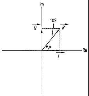
[00142] FIG. 1 illustrates a phasor representation R 102 of a signal r(t). A
phasor
representation of a signal is explicitly representative of the magnitude of
the signal's
CA 02650532 2008-10-24
WO 2007/133323 PCT/US2007/006197
-18-
envelope and of the signal's phase shift relative to a reference signal. In
this
document, for purposes of convenience, and not limitation, the reference
signal is
defined as being aligned with the real (Re) axis of the orthogonal space of
the phasor
representation. The invention is not, however, limited to this embodiment. The
frequency information of the signal is implicit in the representation, and is
given by
the frequency of the reference signal. For example, referring to FIG. 1, and
assuming
that the real axis corresponds to a cos(cot) reference signal, phasor R would
translate
to the function r(t) = R(t) cos(c)t +0(t)), where R is the magnitude of R
[00143] Still referring to FIG. 1, it is noted that phasor R can be decomposed
into a
real part phasor I and an imaginary part phasor Q. I and Q are said to be the
in-
phase and quadrature phasor components of R with respect to the reference
signal. It
is further noted that the signals that correspond to I and Q are related to
r(t) as
I(t)=R(t)=cos(O(t)) and Q(t)=R(t)-sin(O(t)), respectively. In the time domain,
signal r(t)
can also be written in terms of its in-phase and quadrature components as
follows:
r(t) = I(t)-cos(wt) + Q(t)-sin(c)t) _
R(t)-cos(O(t))-cos(cot) + R(t)-sin(O(t))-sin(c)t) (1)
[00144] Note that, in the example of FIG. 1, R(t) is illustrated at a
particular instant of
time.
2.2) Time-Varying Complex Envelope Signals
[00145] FIG. 2 illustrates a phasor representation of a signal r(t) at two
different
instants of time tl and Q. It is noted that the magnitude of the phasor, which
represents the magnitude of the signal's envelope, as well as its relative
phase shift
both vary from time tl to time Q. In FIG. 2, this is illustrated by the
varying
magnitude of phasors RI and R2 and their corresponding phase shift angles 01
and
02. Signal r(t), accordingly, is a time-varying complex envelope signal.
CA 02650532 2008-10-24
WO 2007/133323 PCT/US2007/006197
-19-
[00146] It is further noted, from FIG. 2, that the real and imaginary phasor
components
of signal r(t) are also time-varying in amplitude. Accordingly, their
corresponding
time domain signals also have time-varying envelopes.
[00147] FIGs. 3A-3C illustrate an example modulation to generate a time-
varying
complex envelope signal. FIG. 3A illustrates a view of a signal m(t). FIG. 3B
illustrates a view of a portion of a carrier signal c(t). FIG. 3C illustrates
a signal r(t)
that results from the multiplication of signals m(t) and c(t).
[00148] In the example of FIG. 3A, signal m(t) is a time-varying magnitude
signal.
m(t) further undergoes a zero crossing. Carrier signal c(t), in the example of
FIG. 3B,
oscillates at some carrier frequency, typically higher than that of signal
m(t).
[00149] From FIG. 3C, it can be noted that the resulting signal r(t) has a
time-varying
envelope. Further, it is noted, from FIG. 3C, that r(t) undergoes a reversal
in phase at
the moment when the modulating signal m(t) crosses zero. Having both non-
constant
envelope and phase, r(t) is said to be a time-varying complex envelope signal.
2.3) Constant Envelope Decomposition of Time-Varying Envelope Signals
[00150] Any phasor of time-varying magnitude and phase can be obtained by the
sum
of two or more constant magnitude phasors having appropriately specified phase
shifts relative to a reference phasor.
[00151] FIG. 3D illustrates a view of an example time-varying envelope and
phase
signal S(t). For ease of illustration, signal S(t) is assumed to be a
sinusoidal signal
having a maximum envelope magnitude A. FIG. 3D further shows an example of
how signal S(t) can be obtained, at any instant of time, by the sum of two
constant
envelope signals S1(t) and S2(t). Generally, Sj(t)=Ajsin(wt+0j(t)) and
S I (t)=A2sin(t,t)t+02(t)).
[00152] For the purpose of illustration, three views are provided in FIG. 3D
that
illustrate how by appropriately phasing signals SI(t) and S2(t) relative to
S(t), signals
SI(t) and SZ(t) can be summed so that S(t)=K(S1(t)+S2(t)) where K is a
constant. In
other words, signal S(t) can be decomposed, at any time instant, into two or
more
signals. From FIG. 3D, over period T,, St(t) and S2(t) are both in-phase
relative to
signal S(t), and thus sum to the maximum envelope magnitude A of signal S(t).
Over
CA 02650532 2008-10-24
WO 2007/133323 PCT/US2007/006197
-20-
period T3, however, signals Si(t) and S2(t) are 180 degree out-of-phase
relative to
each other, and thus sum to a minimum envelope magnitude of signal S(t).
[00153] The example of FIG. 3D illustrates the case of sinusoidal signals. A
person
skilled in the art, however, will understand that any time-varying envelope,
which
modulates a carrier signal that can be represented by a Fourier series or
Fourier
transform, can be similarly decomposed into two or more substantially constant
envelope signals. Thus, by controlling the phase of a plurality of
substantially
constant envelope signals, any time-varying complex envelope signal can be
generated.
Vector Power Amplification Methods and Systems
[00154] Vector power amplification methods and systems according to
embodiments
of the present invention rely on the ability to decompose any time-varying
envelope
signal into two or more substantially constant envelope constituent signals or
to
receive or generate such constituent signals, amplify the constituent signals,
and then
sum the amplified signals to generate an amplified version of the time-varying
complex envelope signal.
[00155] In sections 3.1-3.3, vector power amplification (VPA) embodiments of
the
present invention are provided, including 4-branch and 2-branch embodiments.
In the
description, each VPA embodiment is first presented conceptually using a
mathematical derivation of underlying concepts of the embodiment. An
embodiment
of a method of operation of the VPA embodiment is then presented, followed by
various system level embodiments of the VPA embodiment.
[00156] Section 3.4 presents various embodiments of control modules according
to
embodiments of the present invention. Control modules according to embodiments
of
the present invention may be used to enable certain VPA embodiments of the
present
invention. In some embodiments, the control modules are intermediary between
an
input stage of the VPA embodiment and a subsequent vector modulation stage of
the
WA embodiment.
[00157] Section 3.5 describes VPA output stage embodiments according to
embodiments of the present invention. Output stage embodiments are directed to
generating the output signal of a VPA embodiment.
CA 02650532 2008-10-24
WO 2007/133323 PCT/US2007/006197
-21 -
[00158] Section 3.6 is directed to harmonic control according to embodiments
of the
present invention. Harmonic control may be implemented in certain embodiments
of
the present invention to manipulate the real and imaginary power in the
harmonics of
the VPA embodiment, thus increasing the power present in the fundamental
frequency
at the output.
[00159] Section 3.7 is directed to power control according to embodiments of
the
present invention. Power control may be implemented in certain embodiments of
the
present invention in order to satisfy power level requirements of applications
where
VPA embodiments of the present invention may be employed.
3.1) Cartesian 4-Branch Vector Power Amplifier
[00160] According to one embodiment of the invention, herein called the
Cartesian 4-
Branch VPA embodiment for ease of illustration and not limitation, a time-
varying
complex envelope signal is decomposed into 4 substantially constant envelope
constituent signals. The constituent signals are equally or substantially
equally
amplified individually, and then summed to construct an amplified version of
the
original time-varying complex envelope signal.
[00161] It is noted that 4 branches are employed in this embodiment for
purposes of
illustration, and not limitation. The scope of the invention covers use of
other
numbers of branches, and implementation of such variations will be apparent to
persons skilled in the art based on the teachings contained herein.
[00162] In one embodiment, a time-varying complex envelope signal is first
decomposed into its in-phase and quadrature vector components. In phasor
representation, the in-phase and quadrature vector components correspond to
the
signal's real part and imaginary part phasors, respectively.
1001631 As described above, magnitudes of the in-phase and quadrature vector
components of a signal vary proportionally to the signal's magnitude, and are
thus not
constant envelope when the signal is a time-varying envelope signal.
Accordingly,
the 4-Branch VPA embodiment further decomposes each of the in-phase and
quadrature vector components of the signal into four substantially constant
envelope
CA 02650532 2008-10-24
WO 2007/133323 PCT/US2007/006197
-22-
components, two for the in-phase and two for the quadrature signal components.
This
concept is illustrated in FIG. 4 using a phasor signal representation.
[00164] In the example of FIG. 4, phasors I' and I2 correspond to the real
part
phasors of an exemplary time-varying complex envelope signal at two instants
of time
tl and t2, respectively. It is noted that phasors II and 12 have different
magnitudes.
[00165] Still referring to FIG. 4, at instant tl, phasor I~ can be obtained by
the sum of
upper and lower phasors I ul and I4 . Similarly, at instant t2, phasor I z can
be
obtained by the sum of upper and lower phasors I U2 and IL2 . Note that
phasors I U,
and I U2 have equal or substantially equal magnitude. Similarly, phasors 'r,
and
I
IL2 have substantially equal magnitude. Accordingly, the real part phasor of
the
time-varying envelope signal can be obtained at any time instant by the sum of
at least
two substantially constant envelope components.
[001661 The phase shifts of phasors I U, and I,, relative to I1, as well as
the phase
shifts of phasors I UZ and IL2 relative to I2 are set according to the desired
magnitude of phasors I1 and I2 , respectively. In one case, when the upper and
lower phasors are selected to have equal magnitude, the upper and lower
phasors are
symmetrically shifted in phase relative to the phasor. This is illustrated in
the
example of FIG. 4, and corresponds to I ul , I4 , I U= , and IL2 all having
equal
magnitude. In a second case, the phase shift of the upper and lower phasors
are
substantially symmetrically shifted in phase relative to the phasor. Based on
the
description herein, anyone skilled in the art will understand that the
magnitude and
phase shift of the upper and lower phasors do not have to be exactly equal in
value
CA 02650532 2008-10-24
WO 2007/133323 PCT/US2007/006197
-23-
[00167] As an example, it can be further verified that, for the case
illustrated in FIG. 4,
ol 02
the relative phase shifts, illustrated as 2 and 2 in FIG. 4, are related to
the
magnitudes of normalized phasors I1 and I z as follows:
cot-' and (2)
2 2
2 1 - I'-
4
2 = cot-' I2 , (3)
2 z
2 1-IZ
4
[00168] wherein I, and IZ represent the normalized magnitudes of phasors It
and 12,
respectively, and wherein the domains of I1 and I2 are restricted
appropriately
according to the domain over which equation (2) and (3) are valid. It is noted
that
equations (2) and. (3) are one representation for relating the relative phase
shifts to the
normalized magnitudes. Other, solutions, equivalent representations, and/or
simplified representations of equations (2) and (3) may also be employed. Look
up
tables relating relative phase shifts to riormalized magnitudes may also be
used.
[00169] The concept describe above can be similarly applied to the imaginary
phasor
or the quadrature component part of a signal r(t) as illustrated in FIG. 4.
Accordingly,
at any time instant t, imaginary phasor part Q of signal r(t) can be obtained
by
summing upper and lower phasor components Qu and QL of substantially equal and
constant magnitude. In this example, Qu and QL are symmetrically shifted in
phase
relative to Q by an angle set according to the magnitude of Q at time t. The
relationship of Qu and QL to the desired phasor Q are related as defined in
equations
2 and 3 by substituting Q1 and Q2 for Ii and 12 respectively.
CA 02650532 2008-10-24
WO 2007/133323 PCT/US2007/006197
-24-
[00170] It follows from the above discussion that, in phasor representation,
any phasor
R of variable magnitude and phase can be constructed by the sum of four
substantially constant magnitude phasor components:
R=Iu+I". +Qu+QL;
Iu + IL = I;
Qu + QL = Q; (4)
lu =1L = constant;
Qu = QL = constant;
where Iu, IL, Qu, and QL represent the magnitudes of phasors Iu ~ I c= Qu ,
and Qc ,
respectively.
[00171] Correspondingly, in the time domain, a time-varying complex envelope
sinusoidal signal r(t) = R(t) cos(wt +0) is constructed by the sum of four
constant
envelope signals as follows:
r(t) = Iu (t)+Ic(t)+Qu(t)+Qc(t);
Iu (t) = sgn(I) x Iu x cos( ' ) x cos(wt) + Iu x sin( ' ) x sin(tvt);
2 2
IL (t) = sgn(I) x 'L x cos( 2' ) x cos(twt) - IL x sin( ' ) x sin(wt); (5)
Qu (t) = - sgn(Q) x Qu x cos( ~2 ) x sin(wt) + Qu x sin( ~~ ) x cos(wt);
QL (t) =-sgn(g) x Qt x cos(~2 ) x sin(wt) Q
-L x sin(~2 ) x cos(wt).
where sgn( I)= 1 depending on whether I is in-phase or 180 degrees out-of-
phase
with the positive real axis. Similarly, sgn( Q)= 1 depending on whether Q is
in-
ol
phase or 180 degrees out-of-phase with the imaginary axis. 2 corresponds to
the
OQ
phase shift of Iu and IL relative to the real axis. Similarly, 2 corresponds
to the
o, OQ
phase shift of Qu and QL relative to the imaginary axis. 2 and 2 can be
calculated using the equations given in (2) and (3).
CA 02650532 2008-10-24
WO 2007/133323 PCT/US2007/006197
- 25 -
[00172] Equations (5) can be further simplified as:
r(t) = Iu (t) + IL (t) + Qu (t) + Qc (t);
Iu (t) = sgn(I) x IuX x cos(wt) + Iu,, x sin(o)t);
I,, (t) = sgn(I) x IuX x cos(wt) - Iu,, x sin(wt); (6) where
Qu (t) =-QuX x cos(wt) + sgn(g) x Q. x sin(wt);
QL (t) = Q. x cos(wt) - sgn(Q) x Q,, x sin(wt).
IuX = Iu x cos(' )= IL x cos(' ) IuY = Iu x sin(' ) IL x sin(L)
2 2 2 2
QUx =QU xsin(OQ)=QL xsin(og) QU3, =Qu xcos(OQ)=QL xcos(Og)
2 2 and 2 2
[00173] It can be understood by a person skilled in the art that, whereas the
time
domain representations in equations (5) and (6) have been provided for the
case of a
sinusoidal waveform, equivalent representations can be developed for non-
sinusoidal
waveforms using appropriate basis functions. Further, as understood by a
person
skilled in the art based on the teachings herein, the above-describe two-
dimensional
decomposition into substantially constant envelope signals can be extended
appropriately into a multi-dimensional decomposition.
[00174] FIG. 5 is an example block diagram of the Cartesian 4-Branch VPA
embodiment. An output signal r(t) 578 of desired power level and frequency
characteristics is generated from baseband in-phase and quadrature components
according to the Cartesian 4-Branch VPA embodiment.
[00175] In the example of FIG. 5, a frequency generator such as a synthesizer
510
generates a reference signal A*cos(wt) 511 having the same frequency as that
of
output signal r(t) 578. It can be understood by a person skilled in the art
that the
choice of the reference signal is made according to the desired output signal.
For
example, if the desired frequency of the desired output signal is 2.4 GHz,
then the
frequency of the reference signal is set to be 2.4 GHz. In this manner,
embodiments
of the invention achieve frequency up-conversion.
[00176] Referring to FIG. 5, one or more phase splitters are used to generate
signals
521, 531, 541, and 551 based on the reference signal 511. In the example of
FIG. 5,
this is done using phase splitters 512, 514, and 516 and by applying 0 phase
shifts at
CA 02650532 2008-10-24
WO 2007/133323 PCT/US2007/006197
-26-
each of the phase splitters. A person skilled in the art will appreciate,
however, that
various techniques may be used for generating signals 521, 531, 541, and 551
of the
reference signal 511. For example, a 1:4 phase splitter may be used to
generate the
four replicas 521, 531, 541, and 551 in a single step or in the example
embodiment of
FIG 5, signal 511 can be directly coupled to signals 521, 531, 541, 551
Depending on
the embodiment, a variety of phase shifts may also be applied to result in the
desired
signals 521, 531, 541, and 551.
[00177) Still referring to FIG. 5, the signals 521, 531, 541, and 551 are each
provided
to a corresponding vector modulator 520, 530, 540, and 550, respectively.
Vector
modulators 520, 530, 540, and 550, in conjunction with their appropriate input
signals, generate four constant envelope constituents of signal r(t) according
to the
equations provided in (6). In the example embodiment of FIG. 5, vector
modulators
520 and 530 generate the Iu(t) and IL(t) components, respectively, of signal
r(t).
Similarly, vector modulators 540 and 550 generate the Qu(t) and QL(t)
components,
respectively, of signal r(t).
[00178] The actual implementation of each of vector modulators 520, 530, 540,
and
550 may vary. It will be understood by a person skilled in the art, for
example, that
various techniques exist for generating the constant envelope constituents
according
to the equations in (6).
[00179] In the example embodiment of FIG. 5, each of vector modulators 520,
530,
540, 550 includes an input phase splitter 522, 532, 542, 552 for phasing the
signals
522, 531, 541, 551. Accordingly, input phase splitters 522, 532, 542, 552 are
used to
generate an in-phase and a quadrature components or their respective input
signals.
[00180] In each vector modulator 520, 530, 540, 550, the in-phase and
quadrature
components are multiplied with amplitude information. In FIG. 5, for example,
multiplier 524 multiplies the quadrature component of signal 521 with the
quadrature
amplitude information IUY of Iu(t). In parallel, multiplier 526 multiplies the
in-phase
replica signal with the in-phase amplitude information sgn(I)xlux of Iu(t).
[00181] To generate the Iu(t) constant envelope constituent signals 525 and
527 are
summed using phase splitter 528 or alternate summing techniques. The resulting
signal 529 corresponds to the IU(t) component of signal r(t).
CA 02650532 2008-10-24
WO 2007/133323 PCT/US2007/006197
-27-
[00182] In similar fashion as described above, vector modulators 530, 540, and
550,
respectively, generate the IL(t), Qu(t), and QL(t) components of signal r(t).
IL(t),
Qu(t), and QL(t), respectively, correspond to signals 539, 549, and 559 in
FIG. 5.
[00183] Further, as described above, signals 529, 539, 549, and 559 are
characterized
by having substantially equal and constant magnitude envelopes. Accordingly,
when
signals 529, 539, 549, and 559 are input into corresponding power amplifiers
(PA)
562, 564, 566, and 568, corresponding amplified signals 563, 565, 567, and 569
are
substantially constant envelope signals.
[00184] Power amplifiers 562, 564, 566, and 568 amplify each of the signals
529, 539,
549, 559, respectively. In an embodiment, substantially equal power
amplification is
applied to each of the signals 529, 539, 549, and 559. In an embodiment, the
power
amplification level of PAs 562, 564, 566, and 568 is set according to the
desired
power level of output signal r(t).
[00185] Still referring to FIG. 5, amplified signals 563 and 565 are summed
using
summer 572 to generate an amplified version 573 of the in-phase component I(t)
of
signal r(t). Similarly, amplified signals 567 and 569 are summed using summer
574
to generate an amplified version 575 of the quadrature component Q(t) of
signal r(t).
[00186] Signals 573 and 575 are summed using summer 576, as shown in FIG. 5,
with
the resulting signal corresponding to desired output signal r(t).
[00187] It must be noted that, in the example of FIG. 5, summers 572, 574, and
576 are
being used for the purpose of illustration only. Various techniques may be
used to
sum amplified signals 563, 565, 567, and 569. For example, amplified signals
563,
565, 567, and 569 may be summed all in one step to result in signal 578. In
fact,
according to various VPA embodiments of the present invention, it suffices
that the
summing is done after amplification. Certain VPA embodiments of the present
invention, as will be further described below, use minimally lossy summing
techniques such as direct coupling via wire. Alternatively, certain VPA
embodiments
use conventional power combining techniques. In other embodiments, as will be
further described below, power amplifiers 562, 564, 566, and 568 can be
implemented
as a multiple-input single-output power amplifier.
CA 02650532 2008-10-24
WO 2007/133323 PCT/US2007/006197
-28-
[00188] Operation of the Cartesian 4-Branch VPA embodiment shall now be
further
described with reference to the process flowchart of FIG. 6. The process
begins at
step 610, which includes receiving the baseband representation of the desired
output
signal. In an embodiment, this involves receiving in-phase (I) and quadrature
(Q)
components of the desired output signal. In another embodiment, this involves
receiving magnitude and phase of the desired output signal. In an embodiment
of the Cartesian 4-Branch VPA embodiment, the I and Q are baseband components.
In
another embodiment, the I and Q are RF components and are down-converted to
baseband.
[00189] Step 620 includes receiving a clock signal set according to a desired
output
signal frequency of the desired output signal. In the example of FIG. 5, step
620 is
achieved by receiving reference signal 511.
[00190] Step 630 includes processing the I component to generate first and
second
signals having the output signal frequency. The first and second signals have
substantially constant and equal magnitude envelopes and a sum equal to the I
component. The first and second signals correspond to the Iu(t) and IL(t)
constant
envelope constituents described above. In the example of FIG. 5, step 630 is
achieved
by vector modulators 520 and 530, in conjunction with their appropriate input
signals.
[00191] Step 640 includes processing the Q component to generate third and
fourth
signals having the output signal frequency. The third and fourth signals have
substantially constant and equal magnitude envelopes and a sum equal to the Q
component. The third and fourth signals correspond to the Qu(t) and QL(t)
constant
envelope constituents described above. In the example of FIG. 5, step 630 is
achieved
by vector modulators 540 and 550, in conjunction with their appropriate input
signals.
[00192] Step 650 includes individually amplifying each of the first, second,
third, and
fourth signals, and summing the amplified signals to generate the desired
output
signal. In an embodiment, the amplification of the first, second, third, and
fourth
signals is substantially equal and according to a desired power level of the
desired
output signal. In the example of FIG. 5, step 650 is achieved by power
amplifiers
562, 564, 566, and 568 amplifying respective signals 529, 539, 549, and 559,
and by
summers 572, 574, and 576 sununing amplified signals 563, 565, 567, and 569 to
generate output signa1578.
CA 02650532 2008-10-24
WO 2007/133323 PCT/US2007/006197
-29-
[00193] FIG. 7A is a block diagram that illustrates an exemplary embodiment of
a
vector power amplifier 700 implementing the process flowchart 600 of FIG. 6.
In the
example of FIG. 7A, optional components are illustrated with dashed lines. In
other
embodiments, additional components may be optional.
[00194] Vector power amplifier 700 includes an in-phase (I) branch 703 and a
quadrature (Q) branch 705. Each of the I and Q branches further comprises a
first
branch and a second branch.
[00195] In-phase (I) information signal 702 is received by an I Data Transfer
Function
module 710. In an embodiment, I information signal 702 includes a digital
baseband
signal. In an embodiment, I Data Transfer Function module 710 samples I
information signal 702 according to a sample clock 706. In another embodiment,
I
information signal 702 includes an analog baseband signal, which is converted
to
digital using an analog-to-digital converter (ADC) (not shown in FIG. 7A)
before
being input into I Data Transfer Function module 710. In another embodiment, I
information signal 702 includes an analog baseband signal which input in
analog form
into I Data Transfer Function module 710, which also includes analog
circuitry. In
another embodiment, I information signal 702 includes a RF signal which is
down-
converted to baseband before being input into I Data Transfer Function module
710
using any of the above described embodiments.
[00196] I Data Transfer Function module 710 processes I information signal
702, and
determines in-phase and quadrature amplitude information of at least two
constant
envelope constituent signals of I information signal 702. As described above
with
reference to FIG. 5, the in-phase and quadrature vector modulator input
amplitude
information corresponds to sgn(I)xlux and IuY, respectively. The operation of
I Data
Transfer Function module 710 is further described below in section 3.4.
[00197] I Data Transfer Function module 710 outputs information signals 722
and 724
used to control the in-phase and quadrature amplitude components of vector
modulators 760 and 762. In an embodiment, signals 722 and 724 are digital
signals.
Accordingly, each of signals 722 and 724 is fed into a corresponding digital-
to-analog
converter (DAC) 730 and 732, respectively. The resolution and sample rate of
DACs
730 and 732 is selected to achieve the desired I component of the output
signal 782.
DACs 730 and 732 are controlled by DAC clock signals 723 and 725,
respectively.
CA 02650532 2008-10-24
WO 2007/133323 PCT/US2007/006197
-30-
DAC clock signals 723 and 725 may be derived from a same clock signal or may
be
independent.
[00198] In another embodiment, signals 722 and 724 are analog signals, and
DACs
730 and 732 are not required.
[00199] In the exemplary embodiment of FIG. 7A, DACs 730 and 732 convert
digital
infonmation signals 722 and 724 into corresponding analog signals, and input
these
analog signals into optional interpolation filters 731 and 733, respectively.
Interpolation filters 731 and 733, which also serve as anti-aliasing filters,
shape the
DACs outputs to produce the desired output waveform. Interpolation filters 731
and
733 generate signals 740 and 742, respectively. Signal 741 represents the
inverse of
signal 740. Signals 740-742 are input into vector modulators 760 and 762.
[00200] Vector modulators 760 and 762 multiply signals 740-742 with
appropriately
phased clock signals to generate constant envelope constituents of I
information
signal 702. The clock signals are derived from a channel clock signal 708
having a
rate according to a desired output signal frequency. A plurality of phase
splitters,
such as 750 and 752, for example, and phasors associated with the vector
modulator
multipliers may be used to generate the appropriately phased clock signals.
[00201] In the embodiment of FIG. 7A, for example, vector modulator 760
modulates
a 90 shifted channel clock signal with quadrature amplitude information
signal 740.
In parallel, vector modulator 760 modulates an in-phase channel clock signal
with in-
phase amplitude information signal 742. Vector modulator 760 combines the two
modulated signals to generate a first modulated constant envelope constituent
761 of I
information signal 702. Similarly, vector modulator 762 generates a second
modulated constant envelope constituent 763 of I information signal 702, using
signals 741 and 742. Signals 761 and 763 correspond, respectively, to the
IU(t) and
IL(t) constant envelope components described with reference to FIG. 5.
[00202] In parallel and in similar fashion, the Q branch of vector power
amplifier 700
generates at least two constant envelope constituent signals of quadrature (Q)
information signal 704.
[00203] In the embodiment of FIG. 7A, for example, vector modulator 764
generates a
first constant envelope constituent 765 of Q information signal 704, using
signals 744
CA 02650532 2008-10-24
WO 2007/133323 PCT/US2007/006197
-31-
and 746. Similarly, vector modulator 766 generates a second constant envelope
constituent 767 of Q information signal 704, using signals 745 and 746.
[00204] As described above with respect to FIG. 5, constituent signals 761,
763, 765,
and 767 have substantially equal and constant magnitude envelopes. In the
exemplary
embodiment of FIG. 7A, signals 761, 763, 765, and 767 are, respectively, input
into
corresponding power amplifiers (PAs) 770, 772, 774, and 776. PAs 770, 772,
774,
and 776 can be linear or non-linear power amplifiers. In an embodiment, PAs
770,
772, 774, and 776 include switching power amplifiers.
[00205] Circuitry 714 and 716 (herein referred to as "autobias circuitry" for
ease of
reference, and not limitation) and in this embodiment, control the bias of PAs
770,
772, 774, and 776 according to I and Q information signals 702 and 704. In the
embodiment of FIG. 7A, autobias circuitry 714 and 716 provide, respectively,
bias
signals 715 and 717 to PAs 770, 772 and PAs 774, 776. Autobias circuitry 714
and
716 are further described below in section 3.5. Embodiments of PAs 770, 772,
774,
and 776 are also discussed below in section 3.5.
[00206] In an embodiment, PAs 770, 772, 774, and 776 apply substantially equal
power amplification to respective substantially constant envelope signals 761,
763,
765, and 767. In other embodiments, PA drivers are additionally employed to
provide
additional power amplification. In the embodiment of FIG. 7A, PA drivers 794,
795,
796, and 797 are optionally added between respective vector modulators 760,
762,
764 766 and respective PAs 770, 772, 774, and 776, in each branch of vector
power
amplifier 700.
[00207] The outputs of PAs 770, 772, 774, and 776 are coupled together to
generate
output signal 782 of vector power amplifier 700. In an embodiment, the outputs
of
PAs 770, 772, 774, and 776 are directly coupled together using a wire. Direct
coupling in this manner means that there is minimal or no resistive,
inductive, or
capacitive isolation between the outputs of PAs 770, 772, 774, and 776. In
other
words, outputs of PAs 770, 772, 774, and 776, are coupled together without
intervening components. Alternatively, in an embodiment, the outputs of PAs
770,
772,. 774, and 776 are coupled together indirectly through inductances and/or
capacitances that result in low or minimal impedance connections, and/or
connections
that result in minimal isolation and minimal power loss. Alternatively,
outputs of PAs
CA 02650532 2008-10-24
WO 2007/133323 PCT/US2007/006197
-32-
770, 772, 774, and 776 are coupled using well known combining techniques, such
as
Wilkinson, hybrid, transformers, or known active combiners. In an embodiment,
the
PAs 770, 772, 774, and 776 provide integrated amplification and power
combining in,
a single operation. In an embodiment, one or more of the power amplifiers
and/or
drivers described herein are implemented using multiple input, single output
power
amplification techniques, examples of which are shown in FIGS. 7B, and 51 A-H.
1002081 Output signal 782 includes the I and Q characteristics of I and Q
information
signals 702 and 704. Further, output signal 782 is of the same frequency as
that of its
constituents, and thus is of the desired up-converted output frequency. In
embodiments of vector power amplifier 700, a pull-up impedance 780 is coupled
between the output of vector amplifier 700 and a power supply. Output stage
embodiments according to power amplification methods and systems of the
present
invention will be further described below in section 3.5.
[00209] In other embodiments of vector power amplifier 700, process detectors
are
employed to compensate for any process variations in circuitry of the
amplifier. In
the embodiment of FIG. 7A for example, process detectors 791-793 are
optionally
added to monitor variations in PA drivers 794-797 and phase splitter 750. In
further
embodiments, frequency compensation circuitry 799 may be employed to
compensate
for frequency variations.
[00210] FIG. 7B is a block diagram that illustrates another exemplary
embodiment of
vector power amplifier 700. Optional components are illustrated with dashed
lines,
although other embodiments may have more or less optional components.
[00211] The embodiment illustrates a multiple-input single-output (MISO)
implementation of the amplifier of FIG. 7A. In the embodiment of FIG. 7B,
constant
envelope signals 761, 763, 765 and 767, output from vector modulators 760,
762, 764,
and 766, are input into MISO PAs 784 and 786. MISO PAs 784 and 786 are two-
input single-output power amplifiers. In an embodiment, MISO PAs 784 and 786
include elements 770, 772, 774, 776, 794-797 as shown in the embodiment of
FIG.
7A or functional equivalence thereof. In another embodiment, MISO PAs 784 and
786 may include other elements, such as optional pre-drivers and optional
process
detection circuitry.. Further, MISO PAs 784 and 786 are not limited to being
two-
input PAs as shown in FIG. 7B. In other embodiments as will be described
further
CA 02650532 2008-10-24
WO 2007/133323 PCT/US2007/006197
-33-
below with reference to FIGs. 51A-H, PAs 784 and 786 can have any number of
inputs and outputs.
[00212] FIG. 8A is a block diagram that illustrates another exemplary
embodiment
800A of a vector power amplifier according to the Cartesian 4-Branch VPA
method
shown in FIG. 6. Optional components are illustrated with dashed lines,
although
other embodiments may have more or less optional components.
[00213] In the embodiment of FIG. 8A, a DAC 830 of sufficient resolution and
sample
rate replaces DACs 730, 732, 734, and 736 of the embodiment of FIG. 7A. DAC
830's sample rate is controlled by a DAC clock signal 826.
[00214] DAC 830 receives in-phase and quadrature information signals 810 and
820
from I Data Transfer Function module 710 and Q Data Transfer Function module
712,
respectively, as described above. In an embodiment, a input selector 822
selects the
order of signals 810 and 820 being input into DAC 830.
[00215] DAC 830 may output a single analog signal at a time. In an embodiment,
a
sample and hold architecture may be used to ensure proper signal timing to the
four
branches of the amplifier, as shown in FIG. 8A.
[00216] DAC 830 sequentially outputs analog signals 832, 834, 836, 838 to a
first set
of sample-and-hold circuits 842, 844, 846, and 848. In an embodiment, DAC 830
is
clocked at a sufficient rate to emulate the operation of DACs 730, 732, 734,
and 736
of the embodiment of FIG. 7A. An output selector 824 determines which of
output
signals 832, 834, 836, and 838 should be selected for output.
[00217] DAC830's DAC clock signal 826, output selector signal 824, input
selector
822, and sample-and-hold clocks 840A-D, and 850 are controlled by a control
module
that can be independent or integrated into transfer function modules 710
and/or 712.
[00218] . In an embodiment, sample-and-hold circuits (S/H) 842, 844, 846, and
848
sample and hold the received analog values from DAC 830 according to a clock
signals 840A-D. Sample-and-hold circuits 852, 854, 856, and 858 sample and
hold the
analog values from sample and hold circuits 842, 844, 846, and 848.
respectively. In
turn, sample-and-hold circuits 852, 854, 856, and 858 hold the received analog
values,
and simultaneously release the values to vector modulators 760, 762, 764, and
766
according to a common clock signal 850. In another embodiment, sample-and-hold
circuits 852, 854, 856, and 858 release the values to optional interpolation
filters 731,
CA 02650532 2008-10-24
WO 2007/133323 PCT/US2007/006197
-34-
733, 735, and 737 which are also anti-aliasing filters. In an embodiment, a
common
clock signal 850 is used in order to ensure that the outputs of S/H 852, 854,
856, and
858 are time-aligned.
[00219] Other aspects of vector power amplifier 800A substantially correspond
to
those described above with respect to vector power amplifier 700.
[00220] FIG. 8B is a block diagram that illustrates another exemplary
embodiment
800B of a vector power amplifier according to the Cartesian 4-Branch VPA
method
shown in FIG. 6. Optional components are illustrated with dashed lines,
although
other embodiments may have more or less optional components.
[00221] Embodiment 800B illustrates another single DAC implementation of the
vector power amplifier. However, in contrast to the embodiment of FIG. 8A, the
sample and hold architecture includes a single set of sample-and-hold (S/H)
circuits.
As shown in FIG. 8B, S/H 842, 844, 846, and 848 receive analog values from DAC
830, illustrated as signals 832, 834, 836, and 838. Each of S/H circuits 842,
844, 846
and 848 release its received value according to a different clock 840A-D as
shown.
The time difference between analog samples used for to generate signals 740,
741,
742, 744, 745, and 746 can be compensated for in transfer functions 710 and
712.
According to the embodiment of FIG. 8B, one level of S/H circuitry can be
eliminated
relative to the embodiment of FIG. 8A, thereby reducing the size and the
complexity
of the amplifier.
[00222] Other aspects of vector power amplifier 800B substantially correspond
to
those described above with respect to vector power amplifiers 700 and 800A.
[00223] FIG. 8C is a block diagram that illustrates another exemplary
embodiment
800C of vector power amplifier 700. Optional components are illustrated with
dashed
lines, although other embodiments may have more or less optional components.
The
embodiment of FIG. 8C illustrates a multiple-input single-output (MISO)
implementation of the amplifier of FIG. 8A. In the embodiment of FIG. 8C,
constant
envelope signals 761, 763, 765 and 767, output from vector modulators 760,
762, 764,
and 766, are input into MISO PAs 860 and 862. MISO PAs 860 and 862 are two-
input single-output power amplifiers. In an embodiment, MISO PAs 860 and 862
include elements 770, 772, 774, 776, 794-797 as shown in the embodiment of
FIG.
7A or functional equivalence thereof. In another embodiment, MISO PAs 860 and
CA 02650532 2008-10-24
WO 2007/133323 PCT/US2007/006197
-35-
862 may include other elements, such as optional pre-drivers and optional
process
detection circuitry. In another embodiment, MISO PAs 860 and 862 may include
other elements, such as pre-drivers, not shown in the embodiment of FIG. 7A.
Further, MISO PAs 860 and 862 are not limited to being two-input PAs as shown
in
FIG. 8C. In other embodiments as will be described further below with
reference to
FIGs. 51A-H, PAs 860 and 862 can have any number of inputs and outputs.
[00224] Other aspects of vector power amplifier 800C substantially correspond
to
those described above with respect to vector power amplifiers 700 and 800A.
.[00225] FIG. 8D is a block diagram that illustrates another exemplary
embodiment
800D of vector power amplifier 700. Optional components are illustrated with
dashed
lines, although other embodiments may have more or less optional components.
The
embodiment of FIG. 8D illustrates a multiple-input single-output (MISO)
implementation of the amplifier of FIG. 8B. In the embodiment of FIG. 8D,
constant
envelope signals 761, 763, 765 and 767, output from vector modulators 760,
762, 764,
and 766, are input into MISO PAs 870 and 872. MISO PAs 870 and 872 are two-
input single-output power amplifiers. In an embodiment, MISO PAs 870 and 872
include elements 770, 772, 774, 776, 794-797 as shown in the embodiment of
FIG.
7A or functional equivalence thereof. In another embodiment, MISO PAs 870 and
872 may include other elements, such as optional pre-drivers and optional
process
detection circuitry. In another embodiment, MISO PAs 870 and 872 may include
other elements, such as pre-drivers, not shown in the embodiment of FIG. 7A.
Further, MISO PAs 870 and 872 are not limited to being two-input PAs as shown
in
FIG. 8D. In other embodiments as will be described further below with
reference to
FIGs. 51 A-H, PAs 870 and 872 can have any number of inputs and outputs.
[00226] Other aspects of vector power amplifier 800D substantially correspond
to
those described above with respect to vector power amplifiers 700 and 800B.
3.2) Cartesian Polar-Cartesian Polar 2-Branch Vector Power Amplifier
[00227] A Cartesian-Polar-Cartesian-Polar (CPCP) 2-Branch VPA embodiment shall
now be described (The name of this embodiment is provided for ease of
reference,
and is not limiting).
CA 02650532 2008-10-24
WO 2007/133323 PCT/US2007/006197
-36-
[00228] According to the Cartesian-Polar-Cartesian-Polar (CPCP) 2-Branch VPA
method, a time-varying complex envelope signal is decomposed into 2
substantially
constant envelope constituent signals. The constituent signals are
individually
amplified, and then summed to construct an amplified version of the original
time-
varying complex envelope signal. In addition, the phase angle of the time-
varying
complex envelope signal is determined and the resulting summation of the
constituent
signals are phase shifted by the appropriate angle.
[00229] In one embodiment of the CPCP 2-Branch VPA method, a magnitude and a
phase angle of a time-varying complex envelope signal are calculated from in-
phase
and quadrature components of a signal. Given the magnitude information, two
substantially constant envelope constituents are calculated from a normalized
version
of the desired time-varying envelope signal, wherein the normalization
includes
implementation specific manipulation of phase and/or amplitude. The two
substantially constant envelope constituents are then phase shifted by an
appropriate
angle related to the phase shift of the desired time-varying envelope signal.
The
substantially constant envelope constituents are then individually amplified
substantially equally, and summed to generate an amplified version of the
original
desired time-varying envelope signal.
[00230] FIGs. 9A and 9B conceptually illustrate the CPCP 2-Branch VPA
embodiment
using a phasor signal representation. In FIG. 9A, phasor R. represents a time-
varying complex envelope input signal r(t). At any instant of time, reflects a
magnitude and a phase shift angle of signal r(t). In the example shown in FIG.
9A,
R;,, is characterized by a magnitude R and a phase shift angle 0. As described
above,
the phase shift angle is measured relative to a reference signal.
[00231] Referring to FIG. 9A, R represents the relative amplitude component of
Rn
generated by U' and L'.
[00232] Still referring to FIG. 9A, it is noted that, at any time instant, R
can be
obtained by the sum of an upper phasor U and a lower phasor L. Further, U and
can be maintained to have substantially constant magnitude. The phasors, U and
CA 02650532 2008-10-24
WO 2007/133323 PCT/US2007/006197
-37-
L, accordingly, represent two substantially constant envelope signals. r(t)
can thus
be obtained, at any time instant, by the sum of two substantially constant
envelope
signals that correspond to phasors U and L.
[00233] The phase shifts of phasors U' and L relative to R are set according
to the
desired magnitude R of R. In the simplest case, when upper and lower phasors U
and L are selected to have equal magnitude, upper and lower phasors U and L
are
substantially symmetrically shifted in phase relative to R. This is
illustrated in the
example of FIG. 9A. It is noted that terms and phrases indicating or
suggesting
orientation, such as but not limited to "upper and lower" are used herein for
ease of
reference and are not functionally or structurally limiting.
[00234] It can be verified that, for the case illustrated in FIG. 9A, the
phase shift of U
0
and L relative to R, illustrated as angle 2 in FIG. 9A, is related to the
magnitude
of R as follows:
2 = cot-' R Z (7)
2
where R represents a normalized magnitude of phasor R.
[00235] Equation (7) can further be reduced to
2 = cos-~ I 2 ~ (7.10)
where R represents a normalized magnitude of phasor R.
[00236] Alternatively, any substantially equivalent mathematical equations or
other
substantially equivalent mathematical techniques such as look up tables can be
used.
CA 02650532 2008-10-24
WO 2007/133323 PCT/US2007/006197
-38-
[00237] It follows from the above discussion that, in phasor representation,
any phasor
R' of variable magnitude and phase can be constructed by the sum of two
constant
magnitude phasor components:
R* = U'+ L (8)
1 U 1=1 L(= A = constant
[00238] Correspondingly, in the time domain, a time-varying envelope
sinusoidal
signal r(t) = R(t)xcos(wt) is constructed by the sum of two constant envelope
signals
as follows:
r'(t) = U ' (t)+L(t);
U '(t ) = A x cos(tvt + 2 (9)
L (t) = Ax cos(wt - 2
0
where A is a constant and 2 is as shown in equation (7).
[00239] From FIG. 9A, it can be further verified that equations (9) can be
rewritten as:
r'(t)=U'(t)+L(t);
U'(t) = C cos(wt) +a sin(wt); (10)
L' (t) = C cos(wt) - Q sin(r.vt);
where C denotes the real part component of phasors U and L and is equal to
0
Axcos( 2). Note that C is a common component of U and i. a and [i denote the
0
imaginary part components of phasors U and L, respectively. a=[3=Axsin( 2).
0
Accordingly, from equations (12), r(t) = 2Cxcos((ot) = 2Axcos( 2)xcos((ot). As
understood by a person skilled in the art based on the teachings herein, other
equivalent and/or simplified representations of the above representations of
the
quantities A, B, and C may also be used, including look up tables, for
example.
CA 02650532 2008-10-24
WO 2007/133323 PCT/US2007/006197
-39-
[00240] Note that R;n is shifted by 9 degrees relative to R. Accordingly,
using
equations (8), it can be deduced that:
=Wepq =(F +l)e'B =U.e'B+lejB (11)
[00241] Equations (11) imply that a representation of R;,, can be obtained by
summing
phasors U and L, described above, shifted by 0 degrees. Further, an amplified
output version, of R,n can be obtained by separately amplifying substantially
equally each of the 0 degrees shifted versions of phasors U and L, and summing
them. FIG. 9B illustrates this concept. In FIG. 9B, phasors U and L represent
0
degrees shifted and amplified versions of phasors U and L. Note that, since U
and L are constant magnitude phasors, U and L are also constant magnitude
phasors. Phasors U and L sum, as shown FIG. 9B, to phasor Roõ, , which is a
power
amplified version of input signal R;n .
[00242] Equivalently, in the time domain, it can be shown that:
r,,,, (t) = U(t) + L(t);
U(t) = K[Ccos(wt + B) + a sin(wt + 6)]; (12)
L(t) = K[C cos(tvt + 9) -P sin(wt + 9)].
where ro,,, (t) corresponds to the time domain signal represented by phasor
Roõ. , U(t)
and L(t) correspond to the time domain signals represents by phasors U and L,
and
K is the power amplification factor.
[00243] A person skilled in the art will appreciate that, whereas the time
domain
representations in equations (9) and (10) have been provided for the case of a
sinusoidal waveform, equivalent representations can be developed for non-
sinusoidal
waveforms using appropriate basis functions.
[00244] FIG. 10 is a block diagram that conceptually illustrates an exemplary
embodiment 1000 of the CPCP 2-Branch VPA embodiment. An output signal r(t) of
CA 02650532 2008-10-24
WO 2007/133323 PCT/US2007/006197
-40-
desired power level and frequency characteristics is generated from in-phase
and
quadrature components according to the CPCP 2-Branch VPA embodiment.
[00245] In the example of FIG. 10, a clock signal 1010 represents a reference
signal
for generating output signal r(t). Clock signal 1010 is of the same frequency
as that of
desired output signal r(t).
[002461 Referring to FIG. 10, an Icik_phase signal 1012 and a Qclk_phase
signal 1014
represent amplitude analog values that are multiplied by the in-phase and
quadrature
components of Clk signal 1010 and are calculated from the baseband I and Q
signals.
[00247] Still referring to FIG. 10, clock signal 1010 is multiplied with
Iclk_phase
signal 1012. In parallel, a 90 degrees shifted version of clock signal 1010
is
multiplied with Qclk_phase signal 1014. The two multiplied signals are
combined to
generate Rclk signal 1016. Rclk signal 1016 is of the same frequency as clock
signal
1010. Further, Rclk signal 1016 is characterized by a phase shift angle
according to
the .ratio of Q(t) and I(t). The magnitude of Rclk signal 1016 is such that
R2clk =
IZclk_phase + QZCIk_phase. Accordingly, Rclk signal 1016 represents a
substantially
constant envelope signal having the phase characteristics of the desired
output signal
r(t).
[00248] Still referring to FIG. 10, Rclk signal 1016 is input, in parallel,
into two vector
modulators 1060 and 1062. Vector modulators 1060 and 1062 generate the U(t)
and
L(t) substantially constant envelope constituents, respectively, of the
desired output
signal r(t) as described in (12). In vector modulator 1060, an in-phase Rclk
signal
1020, multiplied with Common signal 1028, is combined with a 90 degree
shifted
version 1018 of Rclk signal, multiplied with first signal 1026. In parallel,
in vector
modulator 1062, an in-phase Rclk signal 1022, multiplied with Common signal
1028,
is combined with a 90 degrees shifted version 1024 of Rclk signal, multiplied
with
second signal 1030. Common signal 1028, first signal 1026, and second signal
1030
correspond, respectively, to the real part C and the imaginary parts a and 0
described
in equation (12).
[00249] Output signals 1040 and 1042 of respective vector modulators 1060 and
1062
correspond, respectively, to the U(t) and L(t) constant envelope constituents
of input
signal r(t).
CA 02650532 2008-10-24
WO 2007/133323 PCT/US2007/006197
-41-
[00250] As described above, signals 1040 and 1042 are characterized by having
substantially equal and constant magnitude envelopes. Accordingly, when
signals
1040 and 1042 are input into corresponding power amplifiers (PA) 1044 and
1046,
corresponding amplified signals 1048 and 1050 are substantially constant
envelope
signals.
[00251] Power amplifiers 1044 and 1046 apply substantially equal power
amplification
to signals 1040 and 1042, respectively. In an embodiment, the power
amplification
level of PAs 1044 and 1046 is set according to the desired power level of
output
signal r(t). Further, amplified signals 1048 and 1050 are in-phase relative to
each
other. Accordingly, when summed together, as shown in FIG. 10, resulting
signal
1052 corresponds to the desired output signal r(t).
[00252] FIG. l0A is another exemplary embodiment 1000A of the CPCP 2-Branch
VPA embodiment. Embodiment 1000A represents a Multiple Input Single Output
(MISO) implementation of embodiment 1000 of FIG. 10.
[00253] In embodiment 1000A, constant envelope signals 1040 and 1042, output
from
vector modulators 1060 and 1062, are input into MISO PA 1054. MISO PA 1054 is
a
two-input single-output power amplifier. In an embodiment, MISO PA 1054 may
include various elements, such as pre-drivers, drivers, power amplifiers, and
process
detectors (not shown in FIG. 10A), for example. Further, MISO PA 1054 is not
limited to being a two-input PA as shown in FIG. 10A. In other embodiments, as
will
be described further below with reference to FIGs. 51A-H, PA 1054 can have any
number of inputs.
[00254] Operation of the CPCP 2-Branch VPA embodiment is depicted in the
process
flowchart 1100 of FIG. 11.
[00255] The process begins at step 1110, which includes receiving a baseband
representation of the desired output signal. In an embodiment, this involves
receiving
in-phase (I) and quadrature (Q) components of the desired output signal. In
another
embodiment, this involves receiving magnitude and phase of the desired output
signal.
[00256] Step 1120 includes receiving a clock signal set according to a desired
output
signal frequency of the desired output signal. In the example of FIG. 10, step
1120 is
achieved by receiving clock signal 1010.
CA 02650532 2008-10-24
WO 2007/133323 PCT/US2007/006197
-42-
[00257] Step 1130 includes processing the clock signal to generate a
nonmalized clock
signal having a phase shift angle according to the received I and Q
components. In an
embodiment, the normalized clock signal is a constant envelope signal having a
phase
shift angle according to a ratio of the I and Q components. The phase shift
angle of
the normalized clock is -relative to the original clock signal. In the example
of FIG.
10, step 1130 is achieved by multiplying clock signal 1010's in-phase and
quadrature
components with Iclk~_phase 1012 and Qclk_phase 1014 signals, and then summing
the multiplied signal to generate Rclk signal 1016.
[00258] Step 1140 includes the processing of the I and Q components to
generate the
amplitude information required to produce first and second substantially
constant
envelope constituent signals.
[00259] Step 1150 includes processing the amplitude information of step 1140
and the
normalized clock signal Rclk to generate the first and second constant
envelope
constituents of the desired output signal. In an embodiment, step 1150
involves phase
shifting the first and second constant envelope constituents of the desired
output
signal by the phase shift angle of the normalized clock signal. In the example
of FIG.
10, step 1150 is achieved by vector modulators 1060 and 1062 modulating Rclk
signal
1016 with first signal 1026, second signal 1030, and common signal 1028 to
generate
signals 1040 and 1042.
[00260] Step 1160 includes individually amplifying the first and second
constant
envelope constituents, and summing the amplified signals to generate the
desired
output signal. In an embodiment, the amplification of the first and second
constant
envelope constituents is substantially equal and according to a desired power
level of
the desired output signal. In the example of FIG. 10, step 1160 is achieved by
PAs
1044 and 1046 amplifying signals 1040 and 1042 to generate amplified signals
1048
and 1050.
[00261] FIG. 12 is a block diagram that illustrates an exemplary embodiment of
a
vector power amplifier 1200 implementing the process flowchart 1100. Optional
components are illustrated with dashed lines, although in other embodiments
more or
less components may be optional.
[00262] Referring to FIG. 12, in-phase (I) and quadrature (Q) information
signal 1210
is received by an I and Q Data Transfer Function module 1216. In an
embodiment, I
CA 02650532 2008-10-24
WO 2007/133323 PCT/US2007/006197
- 43 -
and Q Data Transfer Function 1216 samples signal 1210 according to a sample
clock
1212. I and Q information signal 1210 includes baseband I and Q information of
a
desired output signal r(t).
[00263] In an embodiment, I and Q Data Transfer Function module 1216 processes
information signal 1210 to generate information signals 1220, 1222, 1224, and
1226.
The operation of I and Q Data Transfer Function module 1216 is further
described
below in section 3.4.
[00264] Referring to FIG. 12, information signal 1220 includes quadrature
amplitude
information of first and second constant envelope constituents of a baseband
version
of desired output signal r(t). With reference to FIG. 9A, for example,
information
signal 1220 includes the a and 0 quadrature components. Referring again to
FIG. 12,
information signal 1226 includes in-phase amplitude information of the first
and
second constant envelope constituents of the baseband version of signal r(t).
With
reference to FIG. 9A, for example, information signal 1226 includes the common
C
in-phase component.
[00265] Still referring to FIG. 12, information signals 1222 and 1224 include
normalized in-phase Iclk_phase and quadrature Qclk_phase signals,
respectively.
Iclk_phase and Qclk_phase are normalized versions of the I and Q information
signals
included in signal 1210. In an embodiment, Iclk_phase and Qclk_phase are
normalized such that that (IZclk_phase + Q2clk_phase = constant). It is noted
that the
phase of signal 1250 corresponds to the phase of the desired output signal and
is
created from Iclk_phase and Qclk_phase. Referring to FIG. 9B, Iclk_phase and
Qclk_phase are related to I and Q as follows:
9 = tan-'(Q) = tan-'(Qdk_Phase ) (12.1)
I Iclt _ Phwe
where 0 represents the phase of the desired output signal, represented b
phasor Ro,,, in FIG. 9B. The sign information of the baseband I and Q
information must be taken into account to calculate 9 for all four quadrants.
[00266] In the exemplary embodiment of FIG. 12, information signals 1220,
1222,
1224, and 1226 are digital signals. Accordingly, each of signals 1220, 1222,
1224,
and 1226 is fed into a corresponding digital-to-analog converter (DAC) 1230,
1232,
CA 02650532 2008-10-24
WO 2007/133323 PCT/US2007/006197
-44-
1234, and 1236. The resolution and sample rate of DACs 1230, 1232, 1234, and
1236
is selected according to specific signaling schemes. DACs 1230, 1232, 1234,
and
1236 are controlled by DAC clock signals 1221, 1223, 1225, and 1227,
respectively.
DAC clock signals 1221, 1223, 1225, and 1227 may be derived from a same clock
signal or may be independent.
[00267] In other embodiments, information signals 1220, 1222, 1224, and 1226
are
generated in analog format and no DACs are required.
[00268] Referring to FIG. 12, DACs 1230, 1232, 1234, and 1236 convert digital
information signals 1220, 1222, 1224, and 1226 into corresponding analog
signals,
and input these analog signal into optional interpolation filters 1231, 1233,
1235, and
1237, respectively. Interpolation filters 1231, 1233, 1235, and 1237, which
also serve
as anti-aliasing filters, shape the DACs output signals to produce the desired
output
waveform. Interpolation filters 1231, 1233, 1235, and 1237 generate signals
1240,
1244, 1246, and 1248, respectively. Signal 1242 represents the inverse of
signal
1240.
[00269] Still referring to FIG. 12, signals 1244 and 1246, which include
Iclk_phase
and Qclk_phase information, are input into a vector modulator 1238. Vector
modulator 1238 multiplies signal 1244 with a channel clock signal 1214.
Channel
clock signal 1214 is selected according to a desired output signal frequency.
In
parallel, vector modulator 1238 multiplies signal 1246 with a 90 shifted
version of
channel clock signal 1214. In other words, vector modulator 1238 generates an
in-
phase component having amplitude of Iclk_phase and a quadrature component
having
amplitude of Qclk_phase.
[00270] Vector modulator 1238 combines the two modulated signals to generate
Rclk
signal 1250. Rclk signal 1250 is a substantially constant envelope signal
having the
desired output frequency and a phase shift angle according to the I and Q data
included in signal 1210.
1002711 Still referring to FIG. 12, signals 1240, 1242, and 1248 include the
U, L, and
Common C amplitude components, respectively, of the complex envelope of signal
r(t). Signals 1240, 1242, and 1248 along with Rclk signal 1250 are input into
vector
modulators 1260 and 1262.
CA 02650532 2008-10-24
WO 2007/133323 PCT/US2007/006197
- 45 -
[00272) Vector modulator 1260 combines signal 1240, multiplied with a 90
shifted
version of Rclk signal 1250, and signal 1248, multiplied with a 0 shifted
version of
Rclk signal 1250, to generate output signal 1264. In parallel, vector
modulator 1262
combines signal 1242, multiplied with a 90 shifted version of Rclk signal
1250, and
signal 1248, modulated with a 0 shifted version of Rclk signal 1250, to
generate
output signal 1266.
[00273] Output signals 1264 and 1266 represent substantially constant envelope
signals. Further, phase shifts of output signals 1264 and 1266 relative to
Rclk signal
1250 are determined by the angle relationships associated with the ratios a/C
and (3/C,
respectively. In an embodiment, a=-(3 and therefore output signals 1264 and
1266 are
symmetrically phased relative to Rclk signal 1250. With reference to FIG. 9B,
for
example, output signals 1264 and 1266 correspond, respectively, to the U and L
constant magnitude phasors.
[00274] A sum of output signals 1264 and 1266 results in a channel-clock-
modulated
signal having the I and Q characteristics of baseband signal r(t). To achieve
a desired
power level at the output of vector power amplifier 1200, however, signals
1264 and
1266 are amplified to generate an amplified output signal. In the embodiment
of FIG.
12, signals 1264 and 1266 are, respectively, input into power amplifiers (PAs)
1270
and 1272 and amplified. In an embodiment, PAs 1270 and 1272 include switching
power amplifiers. Autobias circuitry 1218 controls the bias of PAs 1270 and
1272 as
further described below in section 3.5.2. In the embodiment of FIG. 12, for
example,
autobias circuitry 1218 provides a bias voltage 1228 to PAs 1270 and 1272.
[00275] In an embodiment, PAs 1270 and 1272 apply substantially equal power
amplification to respective constant envelope signals 1264-1266. In an
embodiment,
the power amplification is set according to the desired output power level. In
other
embodiments of vector power amplifier 1200, PA drivers and/or pre-drivers are
additionally employed to provide additional power amplification capability to
the
amplifier. In the embodiment of FIG. 12, for example, PA drivers 1284 and 1286
are
optionally added, respectively, between vector modulators 1260 and 1262 and
subsequent PAs 1270 and 1272.
CA 02650532 2008-10-24
WO 2007/133323 PCT/US2007/006197
-46-
[002761 Respective output signals 1274 and 1276 of PAs 1270 and 1272 are
substantially constant envelope signals. Further, when output signals 1274 and
1276
are summed, the resulting signal has minimal non-linear distortion. In the
embodiment of FIG. 12, output signals 1274 and 1276 are coupled together to
generate output signal 1280 of vector power amplifier 1200. In an embodiment,
no
isolation is used in coupling the outputs of PAs 1270 and 1272. Accordingly,
minimal power 'loss is incurred by the coupling. In an embodiment, the outputs
of
PAs 1270 and 1272 are directly coupled together using a wire. Direct coupling
in this
manner means that there is minimal or no resistive, inductive, or capacitive
isolation
between the outputs of PAs 1270 and 1272. In other words, outputs of PAs 1270
and
1272 are coupled together without intervening components. Alternatively, in an
embodiment, the outputs of PAs 1270 and 1272 are coupled together indirectly
through inductances and/or capacitances that result in low or minimal
impedance
connections, and/or connections that result in minimal isolation and minimal
power
loss. Alternatively, outputs of PAs 1270 - and 1272 are coupled using well
known
combining techniques, such as Wilkinson, hybrid combiners, transformers, or
known
active combiners. In an embodiment, the PAs 1270 and 1272 provide integrated
amplification and power combining in a single operation. In an embodiment, one
or
more of the power amplifiers and/or drivers described herein are implemented
using
multiple input, single output power amplification techniques, examples of
which are
shown in FIGS. 12A, 12B, and 5lA-H.
[00277] Output signal 1280 represents a signal having the I and Q
characteristics of
baseband signal r(t) and the desired output power level and frequency. In
embodiments of vector power amplifier 1200, a pull-up impedance 1288 is
coupled
between the output of vector power amplifier 1200 and a power supply. In other
embodiments, an impedance matching network 1290 is coupled at the output of
vector
power amplifier 1200. Output stage embodiments according to power
amplification
methods and systems of the present invention will be further described below
in
section 3.5.
[002781 In other embodiments of vector power amplifier 1200, process detectors
are
employed to compensate for any process variations in circuitry of the
amplifier. In
CA 02650532 2008-10-24
WO 2007/133323 PCT/US2007/006197
-47-
the exemplary embodiment of FIG. 12, for example, process detector 1282 is
optionally added to monitor variations in PA drivers 1284 and 1286.
[00279] FIG. 12A is a block diagram that illustrates another exemplary
embodiment of
a vector power amplifier 1200A implementing the process flowchart 1100.
Optional
components are illustrated with dashed lines, although in other embodiments
more or
less components may be optional.
[00280] Embodiment 1200A illustrates a multiple-input single-output (MISO)
implementation of embodiment 1200. In embodiment 1200A, constant envelope
signals 1261 and 1263, output from vector modulators 1260 and 1262, are input
into
MISO PA 1292. MISO PA 1292 is a two-input single-output power amplifier. In an
embodiment, MISO PA 1292 includes elements 1270, 1272, 1282, 1284, and 1286 as
shown in the embodiment of FIG. 12. In another embodiment, MISO PA 1292 may
include other elements, such as pre-drivers, not shown in the embodiment of
FIG. 12.
Further, MISO PA 1292 is not limited to being a two-input PA as shown in FIG.
12A.
In other embodiments as will be described further below with reference to
FIGs. 51A-
H, PA 1292 can have any number of inputs and outputs.
[00281] Still referring to FIG. 12A, embodiment 1200A illustrates one
implementation
for delivering autobias signals to MISO PA 1292. In the embodiment of FIG.
12A,
Autobias signal 1228 generated by Autobias circuitry 1218, has one or more
signals
derived from it to bias different stages of MISO PA 1292. As shown in the
example
of FIG. 12A, three bias control signals Bias A, Bias B, and Bias C are derived
from
Autobias signal 1228, and then input at different stages of MISO PA 1292. For
example, Bias C may be the bias signal to the pre-driver stage of MISO PA
1292.
Similarly, Bias B and Bias A may be the bias signals to the driver and PA
stages of
MISO PA 1292.
[00282] In another implementation, shown in embodiment 1200B of FIG. 12 B,
Autobias circuitry 1218 generates separate Autobias signals 1295, 1296, and
1295,
corresponding to Bias A, Bias B, and Bias C, respectively. Signals 1295, 1296,
and
1297 may or may not be generated separately within Autobias circuitry 1218,
but are
output separately as shown. Further, signals 1295, 1296, and 1297 may or may
not be
related as determined by the biasing of the different stages of MISO PA 1294.
CA 02650532 2008-10-24
WO 2007/133323 PCT/US2007/006197
-48-
[00283] Other aspects of vector power amplifiers 1200A and 1200B substantially
correspond to those described above with respect to vector power amplifier
1200.
[00284] FIG. 13 is a block diagram that illustrates another exemplary
embodiment
1300 of a vector power amplifier according to the CPCP 2-Branch VPA
embodiment.
Optional components are illustrated with dashed lines, although in other
embodiments
more or less components may be optional.
[00285] In the exemplary embodiment of FIG. 13, a DAC of sufficient resolution
and
sample rate 1320 replaces DACs 1230, 1232, 1234 and 1236 of the embodiment of
FIG. 12. DAC 1320 is controlled by a DAC clock 1324.
[00286] DAC 1320 receives information signal 1310 from I and Q Data Transfer
Function module 1216. Information signal 1310 includes identical information
content to signals 1220, 1222, 1224 and 1226 in the embodiment of FIG. 12.
[00287] DAC 1320 may output a single analog signal at a time. Accordingly, a
sample-and-hold architecture may be used as shown in FIG. 13.
[00288] DAC 1320 sequentially outputs analog signals 1332, 1334, 1336, 1336 to
a
first set of sample-and-hold circuits 1342, 1344, 1346, and 1348. In an
embodiment,
DAC 1230 is clocked at a sufficient rate to replace DACs 1230, 1232, 1234, and
1236
of the embodiment of FIG. 12. An output selector 1322 determines which of
output
signals 1332, 1334, 1336, and 1338 should be selected for output.
[00289] DAC 1320's DAC clock signal 1324, output selector signal 1322, and
sample-
and-hold clocks 1340A-D and 1350 are controlled by a control module that can
be
independent or integrated into transfer function module 1216.
[00290] In an embodiment, sample-and-hold circuits (S/H) 1342, 1344, 1346, and
1348
hold the received analog values and, according to a clock signal 1340A-D,
release the
values to a second set of sample-and-hold circuits 1352, 1354, 1356, and 1358.
For
example, S/H 1342 release its value to S/H 1352 according to a received clock
signal
1340A. In turn, sample-and-hold circuits 1352, 1354, 1356, and 1358 hold the
received analog values, and simultaneously release the values to interpolation
filters
1231, 1233, 1235, and 1237 according to a common clock signal 1350. A common
clock signal 1350 is used in order to ensure that the outputs of S/H 1352,
1354, 1356,
and 1358 are time-aligned.
CA 02650532 2008-10-24
WO 2007/133323 PCT/US2007/006197
-49-
[00291] In another embodiment, a single layer of S/H circuitry that includes
S/H 1342,
1344, 1346, and 1348 can be employed. Accordingly, S/H circuits 1342, 1344,
1346,
and 1348 receive analog values from DAC 1320, and each releases its received
value
according to a clock independent of the others. For example, S/H 1342 is
controlled
by clock 1340A, which may not be synchronized with clock 1340B that controls
S/H
1344. To ensure that outputs of S/H circuits 1342, 1344, 1346, and 1348 are
time-
aligned, delays between clocks 1340A-D are pre-compensated for in prior stages
of
the amplifier. For example, DAC 1320 outputs signal 1332, 1334, 1336, and 1338
with appropriately selected delays to S/H circuits 1342, 1344, 1346, and 1348
in order
to compensate for the time differences between clocks 1340A-D.
[00292] Other aspects of vector power amplifier 1300 are substantially
equivalent to
those described above with respect to vector power amplifier 1200.
[00293] FIG. 13A is a block diagram that illustrates another exemplary
embodiment
1300A of a vector power amplifier according to the CPCP 2-Branch VPA
embodiment. Optional components are illustrated with dashed lines, although in
other
embodiments more or less components may be optional. Embodiment 1300A is a
MISO implementation of embodiment 1300 of FIG. 13.
[00294] In the embodiment of FIG. 13A, constant envelope signals 1261 and 1263
output from vector modulators 1260 and 1262 are input into MISO PA 1360. MISO
PA 1360 is a two-input single-output power amplifier. In an embodiment, MISO
PA
1360 includes elements 1270, 1272, 1282, 1284, and 1286 as shown in the
embodiment of FIG. 13. In another embodiment, MISO PA 1360 may include other
elements, such as pre-drivers, not shown in the embodiment of FIG. 13, or
functional
equivalents thereof. Further, MISO PA 1360 is not limited to being a two-input
PA as
shown in FIG. 13A. In other embodiments as will be described further below
with
reference to FIGs. 51A-H, PA 1360 can have any number of inputs.
[00295] The embodiment of FIG. 13A further illustrates two different sample
and hold
architectures with a single or two levels of S/H circuitry as shown. The two
implementations have been described above with respect to FIG. 13.
[00296] Embodiment 1300A also illustrates optional bias control circuitry 1218
and
associated bias control signal 1325, 1326, and 1327. Signals 1325, 1326, and
1327
may be used to bias different stages of MISO PA 1360 in certain embodiments.
CA 02650532 2008-10-24
WO 2007/133323 PCT/US2007/006197
-50-
[00297] Other aspects of vector power amplifier 1300A are equivalent to those
described above with respect to vector power amplifiers 1200 and 1300.
3.3) Direct Cartesian 2-Branch Vector Power Amplffier
[00298] A Direct Cartesian 2-Branch VPA embodiment shall now be described.
This
name is used herein for reference purposes, and is not functionally or
structurally
limiting.
[00299) According to the Direct Cartesian 2-Branch VPA embodiment, a time-
varying
envelope signal is decomposed into two constant envelope constituent signals.
The
constituent signals are individually amplified equally or substantially
equally, and
then summed to construct an amplified version of the original time-varying
envelope
signal.
[00300] In one embodiment of the Direct Cartesian 2-Branch VPA embodiment, a
magnitude and a phase angle of a time-varying envelope signal are calculated
from in-
phase and quadrature components of an input signal. Using the magnitude and
phase
information, in-phase and quadrature amplitude components are calculated for
two
constant envelope constituents of the time-varying envelope signal. The two
constant
envelope constituents are then generated, amplified equally or substantially
equally,
and summed to generate an amplified version of the original time-varying
envelope
signal R;,,.
[00301] The concept of the Direct Cartesian 2-Branch VPA will now be described
with
reference to FIGs. 9A and 14.
[00302] As described and verified above with respect to FIG. 9A, the phasor R
can
be obtained by the sum of an upper phasor U and a lower phasor L appropriately
phased to produce R. R is calculated to be proportional to the magnitude Rin.
Further, U and L can be maintained to have substantially constant magnitude.
In
the time domain, U and L represent two substantially constant envelope
signals.
CA 02650532 2008-10-24
WO 2007/133323 PCT/US2007/006197
-51-
The time domain equivalent r(t) of R~ can thus be obtained, at any time
instant, by
the sum of two substantially constant envelope signals.
[00303] For the case illustrated in FIG. 9A, the phase shift of U and L
relative to
0
R, illustrated as angle 2 in FIG. 9A, is related to the magnitude of R as
follows:
cot-' R (13)
2
2 1-
4
where R represents the normalized magnitude of phasor R
[00304] In the time domain, it was shown that a time-varying envelope signal,
r'(t) _
R(t) cos(twt) for example, can be constructed by the sum of two constant
envelope
signals as follows:
r'(t) = U' (t) + L'(t);
U' (t) = C x cos(wt) + a x sin(wt); (14)
L(t) = C x cos(mt) -P x sin(wt).
where C denotes the in-phase amplitude component 'of phasors U and L and is
0
equal or substantially equal 'to Axcos( 2)(A being a constant). a and 0 denote
the
quadrature amplitude components of phasors U and L, respectively.
0
a=(3=Axsin( 2). Note that equations (14) can be modified for non-sinusoidal
signals
by changing the basis function from sinusoidal to the desired function.
[00305] FIG. 14 illustrates phasor R and its two constant magnitude
constituent
phasors U and L. R is shifted by 0 degrees relative to R in FIG. 9A.
Accordingly, it can be verified that:
CA 02650532 2008-10-24
WO 2007/133323 PCT/US2007/006197
-52-
R=RI xe'B =(U'+L)xe'8 =U+L;
U=U xe'B; (15)
L=L xeje.
[00306] From equations (15), it can be further shown that:
U=F xeje =(C+ja)xe'B;
=>U = (C+ ja)(cos8+ jsin9) = (CcosB-asinB)+ j(CsinB+acos8). (16)
[00307] Similarly, it can be shown that:
L=L xe'B =(C+jQ)xe'B;
(17)
=> L =(C+ jQ)(cos9+ jsin0)=(Ccos9-/3sin9)+ j(Csin0+,6 cosB).
[00308] Equations (16) and (17) can be re-written as:
U =(Ccos9-asin8)+ j(CsinB+acos9) =Ux + jUy;
(18)
L = (CcosB-/3sin6)+ j(Csin9+,0 cosB) = Lx + jLy.
[00309] Equivalently, in the time domain:
U(t) = Uxrp, (t) + Uyrp2 (t); (19)
L(t) = Lx4p, (t) + LyV2 (t);
where cpl(t) and cp2(t) represent an appropriately selected orthogonal basis
functions.
[00310] From equations (18) and (19), it is noted that it is sufficient to
calculate the
values of a, 0, C and sin(O) and cos(O) in order to determine the two constant
envelope constituents of a time-varying envelope signal r(t). Further, a, (3
and C can
be entirely determined from magnitude and phase information, equivalently I
and Q
components, of signal r(t).
[00311] FIG. 15 is a block diagram that conceptually illustrates an exemplary
embodiment 1500 of the Direct Cartesian 2-Branch VPA embodiment. An output
signal r(t) of desired power level and frequency characteristics is generated
from in-
phase and quadrature components according to the Direct Cartesian 2-Branch VPA
embodiment.
[00312] In the example of FIG. 15, a clock signal 1510 represents a reference
signal
for generating output signal r(t). Clock signal 1510 is of the same frequency
as that of
desired output signal r(t).
CA 02650532 2008-10-24
WO 2007/133323 PCT/US2007/006197
-53-
[00313] Referring to FIG. 15, exemplary embodiment 1500 includes a first
branch
1572 and a second branch 1574. The first branch 1572 includes a vector
modulator
1520 and a power amplifier (PA) 1550. Similarly, the second branch 1574
includes a
vector modulator 1530 and a power amplifier (PA) 1560.
[00314] Still referring to FIG. 15, clock signal 1510 is input, in parallel,
into vector
modulators 1520 and 1530. In vector modulator 1520, an in-phase version 1522
of
clock signal 1510, multiplied with U., signal 1526, is summed with a 90
degrees
shifted version 1524 of clock signal 1510, multiplied with Uy signal 1528. In
parallel,
in vector modulator 1530, an in-phase version 1532 of clock signal 1510,
multiplied
with Lx signal 1536, is summed with a 90 degrees shifted version 1534 of
clock
signal 1510, multiplied with Ly signal 1538. U. signal 1526 and Uy signal 1528
correspond, respectively, to the in-phase and quadrature amplitude components
of the
U(t) constant envelope constituent of signal r(t) provided in equation (19).
Similarly,
L, signal 1536, and Ly signal 1538 correspond, respectively, to the in-phase
and
quadrature amplitude components of the L(t) constant envelope constituent of
signal
r(t) provided in equation (19).
[00315] Accordingly, respective output signals 1540 and 1542 of vector
modulators
1520 and 1530 correspond, respectively, to the U(t) and L(t) constant envelope
constituents of signal r(t) as described above in equations (19). As described
above,
signals 1540 and 1542 are characterized by having equal and constant or
substantially
equal and constant magnitude envelopes.
[00316] Referring to FIG. 15, to generate the desired power level of output
signal r(t),
signals 1540 and 1542 are input into corresponding power amplifiers 1550 and
1560.
[00317] In an embodiment, power amplifiers 1550 and 1560 apply equal or
substantially equal power amplification to signals 1540 and 1542,
respectively. In an
embodiment, the power amplification level of PAs 1550 and 1560 is set
according to
the desired power level of output signal r(t).
[003181 Amplified output signals 1562 and 1564 are substantially constant
envelope
signals. Accordingly, when summed together, as shown in FIG. 15, resulting
signal
1570 corresponds to the desired output signal r(t).
CA 02650532 2008-10-24
WO 2007/133323 PCT/US2007/006197
-54-
[00319] FIG. 15A is another exemplary embodiment 1500A of the Direct Cartesian
2-
Branch VPA embodiment. Embodiment 1500A represents a Multiple Input Signal
Output (MISO) implementation of embodiment 1500 of FIG. 15.
[003201 In embodiment 1500A, constant envelope signals 1540 and 1542, output
from
vector modulators 1520 and 1530, are input into MISO PA 1580. MISO PA 1580 is
a
two-input single-output power amplifier. Iri an embodiment, MISO PA 1580 may
include various elements, such as pre-drivers, drivers, power amplifiers, and
process
detectors (not shown in FIG. 15A), for example. Further, MISO PA 1580 is not
limited to being a two-input PA as shown in FIG. 15A. In other embodiments, as
will
be described further below with reference to FIGs. 51A-H, PA 1580 can have any
number of inputs.
[00321] Operation of the Direct Cartesian 2-Branch VPA embodiment is depicted
in
the process flowchart 1600 of FIG. 16. The process begins at step 1610, which
includes receiving a baseband representation of a desired output signal. In an
embodiment, the baseband representation includes I and Q components. In
another
embodiment, the I and Q components are RF components that are down-converted
to
baseband.
[00322] Step 1620 includes receiving a clock signal set according to a desired
output
signal frequency of the desired output signal. In the example of FIG. 15, step
1620 is
achieved by receiving clock signal 1510.
[00323] Step 1630 includes processing the I and Q components to generate in-
phase
and quadrature amplitude information of first and second constant envelope
constituent signals of the desired output signal. In the example of FIG. 15,
the in-
phase and quadrature amplitude information is illustrated by U., Uy, L., and
Ly.
[00324] Step 1640 includes processing the amplitude information and the clock
signal
to generate the first and second constant envelope constituent signals of the
desired
output signal. In an embodiment, the first and second constant envelope
constituent
signals are modulated according to the desired output signal frequency. In the
example of FIG. 15, step 1640 is achieved by vector modulators 1520 and 1530,
clock
signal 1510, and amplitude information signals 1526, 1528, 1536, and 1538 to
generate signals 1540 and 1542.
CA 02650532 2008-10-24
WO 2007/133323 PCT/US2007/006197
-55-
[00325] Step 1650 includes amplifying the first and second constant envelope
constituents, and summing the amplified signals to generate the desired output
signal.
In an embodiment, the amplification of the first and second constant envelope
constituents is according to a desired power level of the desired output
signal. In the
example of FIG. 15, step 1650 is achieved by PAs 1550 and 1560 amplifying
respective signals 1540 and 1542 and, subsequently, by the summing of
amplified
signals 1562 and 1564 to generate output signal 1574.
[00326] FIG. 17 is a block diagram that illustrates an exemplary embodiment of
a
vector power amplifier 1700 implementing the process flowchart 1600. Optional
components are illustrated with dashed lines, although other embodiments may
have
more or less optional components.
[00327] Referring to FIG. 17, in-phase (I) and quadrature (Q) information
signal 1710
is received by an I and Q Data Transfer Function module 1716. In an
embodiment, I
and Q Data Transfer Function module 1716 samples signal 1710 according to a
sample clock 1212. 1 and Q information signal 1710 includes baseband I and Q
information.
[00328] In an embodiment, I and Q Data Transfer Function module 1716 processes
information signal 1710 to generate information signals 1720, 1722, 1724, and
1726.
The operation of I and Q Data Transfer Function module 1716 is further
described
below in section 3.4.
[00329] Referring to FIG. 17, information signal 1720 includes vector
modulator 1750
quadrature amplitude information that is processed through DAC 1730 to
generate
signal 1740. Information signal 1722 includes vector modulator 1750 in-phase
amplitude information that is processed through DAC 1732 to generate signal
1742.
Signals 1740 and 1742 are calculated to generate a substantially constant
envelope
signal 1754. With reference to FIG. 14, for example, information signals 1720
and
1722 include the upper quadrature and in-phase components Uy and UX,
respectively.
[00330] Still referring to FIG. 17, information signal 1726 includes vector
modulator
1752 quadrature amplitude information that is processed through DAC 1736 to
generate signal 1746. Information signal 1724 includes vector modulator 1752
in-
phase amplitude information that is processed through DAC 1734 to generate
signal
1744. Signals 1744 and 1746 are calculated to generate a substantially
constant
CA 02650532 2008-10-24
WO 2007/133323 PCT/US2007/006197
-56-
envelope signal 1756. With reference to FIG. 14, for example, information
signals
1724 and 1726 include the lower in-phase and quadrature components L,,, and
Ly,
respectively.
[00331] In the exemplary embodiment of FIG. 17, information signals 1720,
1722,
1724 and 1726 are digital signals. Accordingly, each of signals 1720, 1722,
1724 and
1726 is fed into a corresponding digital-to-analog converter (DAC) 1730, 1732,
1734,
and 1736. The resolution and sample rates of DACs 1730, 1732, 1734, and 1736
are
selected according to the specific desired signaling schemes. DACs 1730, 1732,
1734, and 1736 are controlled by DAC clock signals 1721, 1723, 1725, and 1727,
respectively. DAC clock signals 1721, 1723, 1725, and 1727 may be derived from
a
same clock or may be independent of each other.
[00332] In other embodiments, information signals 1720, 1722, 1724 and 1726
are
generated in analog format and no DACs are required.
[00333] Referring to FIG. 17, DACs 1730, 1732, 1734, and 1736 convert digital
information signals 1720, 1722, 1724, and 1726 into corresponding analog
signals,
and input these analog signals into optional interpolation filters 1731, 1733,
1735, and
1737, respectively. Interpolation filters 1731, 1733, 1735, and 1737, which
also serve
as anti-aliasing filters, shape the DACs output signals to produce the desired
output
waveform. Interpolation filters 1731, 1733, 1735, and 1737 generate signals
1740;
1742, 1744, and 1746, respectively.
[00334] Still referring to FIG. 17, signals 1740, 1742, 1744, and 1746 are
input into
vector modulators 1750 and 1752. Vector modulators 1750 and 1752 generate
first
and second constant envelope constituents. In the embodiment of FIG. 17,
channel
clock 1714 is set according to a desired output signal frequency to thereby
establish
the frequency of the output signal 1770.
[00335] Referring to FIG. 17, vector modulator 1750 combines signal 1740,
multiplied
with a 90 shifted version of channel clock signal 1714, and signal 1742,
multiplied
with a 0 shifted version of channel clock signal 1714, to generate output
signal 1754.
In parallel, vector modulator 1752 combines signal 1746, multiplied with a 90
shifted
version of channel clock signal 1714, and signal 1744, multiplied with a 0
shifted
version of channel clock signal 1714, to generate output signal 1756.
CA 02650532 2008-10-24
WO 2007/133323 PCT/US2007/006197
-57-
[00336] Output signals 1754 and 1756 represent constant envelope signals. A
sum of
output signals 1754 and 1756 results in a carrier signal having the I and Q
characteristics of the original baseband signal.. In embodiments, to generate
a
desired power level at the output of vector power amplifier 1700, signals 1754
and
1756 are amplified and then summed. In the embodiment of FIG. 17, for example,
signals 1754 and 1756 are, respectively, input into corresponding power
amplifiers
(PAs) 1760 and 1762. In an embodiment, PAs 1760 and 1762 include switching
power amplifiers. Autobias circuitry 1718 controls the bias of PAs 1760 and
1762.
In the embodiment of FIG. 17, for example, autobias circuitry 1718 provides a
bias
voltage 1728 to PAs 1760 and 1762.
[00337] In an embodiment, PAs 1760 and 1762 apply equal or substantially equal
power amplification to respective constant envelope signals 1754 and 1756. In
an
embodiment, the power amplification is set according to the desired output
power
level. In other embodiments of vector power amplifier 1700, PA drivers are
additionally employed to provide additional power amplification capability to
the
amplifier. In the embodiment of FIG. 17, for example, PA drivers 1774 and 1776
are
optionally added, respectively, between vector modulators 1750 and 1752 and
subsequent PAs 1760 and 1762.
[00338] Respective output signals 1764 and 1766 of PAs 1760 and 1762 are
substantially constant envelope signals. In the embodiment of FIG. 17, output
signals
1764 and 1766 are coupled together to generate output signal 1770 of vector
power
amplifier 1700. In embodiments, it is noted that the outputs of PAs 1760 and
1762
are directly coupled. Direct coupling in this manner means that there is
minimal or
no resistive, inductive, or capacitive isolation between the outputs of PAs
1760 and
1762. In other words, outputs of PAs 1760 and 1762 are coupled together
without
intervening components. Alternatively, in an embodiment, the outputs of PAs
1760
and 1762 are coupled together indirectly through inductances and/or
capacitances that
result in low or minimal impedance connections, and/or connections that result
in
minimal isolation and minimal power loss. Alternatively, outputs of PAs 1760
and
1762 are coupled using well known combining techniques, such as Wilkinson,
hybrid
couplers, transformers, or known active combiners. In an embodiment, the PAs
1760
and 1762 provide integrated amplification and power combining in a single
operation.
CA 02650532 2008-10-24
WO 2007/133323 PCT/US2007/006197
-58-
In an embodiment, one or more of the power amplifiers and/or drivers described
herein are implemented using multiple input, single output (MISO) power
amplification techniques, examples of which are shown in FIGS. 17A, 17B, and
51A-
H.
[00339] Output signal 1770 represents a signal having the desired I and Q
characteristics of the baseband signal and the desired output power level and
frequency. In embodiments of vector power amplifier 1700, a pull-up impedance
1778 is coupled between the output of vector power amplifier 1700 and a power
supply. In other embodiments, an impedance matching network 1780 is coupled at
the output of vector power amplifier 1700. Output stage embodiments according
to
power amplification methods and systems' of the present invention will be
further
described below in section 3.5.
[00340] In other embodiments of vector power amplifier 1700, process detectors
are
employed to compensate for any process and/or temperature variations in
circuitry of
the amplifier. In the exemplary embodiment of FIG. 17, for example, process
detector 1772 is optionally added to monitor variations in PA drivers 1774 and
1776.
[00341] FIG. 17A is a block diagram that illustrates another exemplary
embodiment
1700A of a vector power amplifier implementing process flowchart 1600.
Optional
components are illustrated with dashed lines, although other embodiments may
have
more or less optional components. Embodiment 1700A illustrates a multiple-
input
single-output (MISO) implementation of the amplifier of FIG. 17. In the
embodiment
of FIG. 17A, constant envelope signals 1754 and 1756, output from vector
modulators
1750 and 1760, are input into MISO PA 1790. MISO PA 1790 is a two-input single-
output power amplifier. In an embodiment, MISO PA 1790 include elements 1760,
1762, 1772, 1774, and 1776 as shown in the embodiment of FIG. 17, or
functional
equivalents thereof. In another embodiment, MISO PA 1790 may include other
elements, such as pre-drivers, not shown in the embodiment of FIG. 17.
Further,
MISO PA 1790 is not limited to being a two-input PA as shown in FIG. 17A. In
other
embodiments, as will be described further below with reference to FIGs. 51A-H,
PA
1790 can have any number of inputs.
[00342] In another embodiment of embodiment 1700, shown as embodiment 1700B of
FIG. 17B, optional Autobias circuitry 1218 generates separate bias control
signals
CA 02650532 2008-10-24
WO 2007/133323 PCT/US2007/006197
-59-
1715, 1717, and 1719, corresponding to Bias A, Bias B, and Bias C,
respectively.
Signals 1715, 1717, and 1719 may or may not be generated separately within
Autobias circuitry 1718, but are output separately as shown. Further, signals
1715,
1717, and 1719 may or may not be related as detennined by the biasing required
for
the different stages of MISO PA 1790.
[00343] FIG. 18 is a block diagram that illustrates another exemplary
embodiment
1800 of a vector power amplifier according to the Direct Cartesian 2-Branch
VPA
embodiment of FIG. 16. Optional components are illustrated with dashed lines,
although other embodiments may have more or less optional components.
[00344] In the exemplary embodiment of FIG. 18, a DAC 1820 of sufficient
resolution
and sample rate replaces DACs 1730, 1732, 1734, and 1736 of the embodiment of
FIG. 17. DAC 1820 is controlled by a DAC clock 1814.
[00345] DAC 1820 receives information signal 1810 from I and Q Data Transfer
Function module 1716. Inforination signal 1810 includes identical information
content to signals 1720, 1722, 1724, and 1726 in the embodiment of FIG. 17.
[00346] DAC 1820 may output a single analog signal at a time. Accordingly, a
sample-and-hold architecture may be used as shown in FIG. 18.
1003471 In the embodiment of FIG. 18, DAC 1820 sequentially outputs analog
signals
1822, 1824, 1826, and 1828 to sample-and-hold circuits 1832, 1834, 1836, and
1838,
respectively. In an embodiment, DAC 1820 is of sufficient resolution and
sample rate
to replace DACs 1720, 1722, 1724, and 1726 of the embodiment of FIG. 17. An
output selector 1812 determines which of output signals 1822, 1824, 1826, and
1828
are selected for output.
[00348] DAC1820's DAC clock signal 1814, output selector signal 1812, and
sample-
and-hold clocks 1830A-D, and 1840 are controlled by a control module that can
be
independent or integrated into transfer function module 1716.
[003491 In an embodiment, sample-and-hold circuits 1832, 1834, 1836, and 1838
sample and hold their respective values and, according to a clock signal 1830A-
D,
release the values to a second set of sample-and-hold circuits 1842, 1844,
1846, and
1848. For example, S/H 1832 release's its value to S/H 1842 according to a
received
clock signal 1830A. In turn, sample-and-hold circuits 1842, 1844, 1846, and
1848
CA 02650532 2008-10-24
WO 2007/133323 PCT/US2007/006197
-60-
hold the received analog values, and simultaneously release the values to
interpolation
filters 1852, 1854, 1856, and 1858 according to a common clock signal 1840.
[00350] In another embodiment, a single set of S/H circuitry that includes S/H
1832,
1834, 1836, and 1838 can be employed. Accordingly, S/H circuits 1832, 1834,
1836,
and 1838 receive analog values from DAC 1820, and each samples and holds its
received value according to independent clocks 1830A-D. For example, S/H 1832
is
controlled by clock 1830A, which may not be synchronized with clock 1830B that
controls S/H 1834. For example, DAC 1820 outputs signals 1822, 1824, 1826, and
1828 with appropriately selected analog values calculated by transfer function
module
1716 to S/H circuits 1832, 1834, 1836, and 1838 in order to compensate for the
time
differences between clocks 1830A-D.
[00351] Other aspects of vector power amplifier 1800 correspond substantially
to those
described above with respect to vector power amplifier 1700.
[00352] FIG. 18A is a block diagram that illustrates another exemplary
embodiment
1800A of a vector power amplifier according to the Direct Cartesian 2-Branch
VPA
embodiment. Optional components are illustrated with dashed lines, although in
other
embodiments more or less components may be optional. Embodiment 1800A is a
Multiple'Input Single Output (MISO) implementation of embodiment 1800 of FIG.
18.
[00353] In the embodiment of FIG. 18A, constant envelope signals 1754 and
1756,
output from vector modulators 1750 and 1752, are input into MISO PA 1860. MISO
PA 1860 is a two-input single-output power amplifier. In an embodiment, MISO
PA
1860 includes elements 1744, 1746, 1760, 1762, and 1772 as shown in the
embodiment of FIG. 18, or functional equivalents thereof. In another
embodiment,
MISO PA 1860 may include other elements, such as pre-drivers, not shown in the
embodiment.of FIG. 17. Further, MISO PA 1860 is not limited to being a two-
input
PA as shown in FIG. 18A. In other embodiments as will be described further
below
with reference to FIGs. 51 A-H, PA 1860 can have any number of inputs.
[00354] The embodiment of FIG. 18A further illustrates two different sample
and hold
architectures with a single or two levels of S/H circuitry as shown. The two
implementations have been described above with respect to FIG. 18.
CA 02650532 2008-10-24
WO 2007/133323 PCT/US2007/006197
-61 -
[00355J Other aspects of vector power amplifier 1800A are substantially
equivalent to
those described above with respect to vector power amplifiers 1700 and 1800.
3.4) I and Q Data to Vector Modulator Transfer Functions
[003561 In some of the above described embodiments, I and Q data transfer
functions
are provided to transform received I and Q data into amplitude information
inputs for subsequent stages of vector modulation and amplification. For
example, in the
embodiment of FIG. 17, I and Q Data Transfer Function module 1716 processes I
and Q information signal 1710 to generate in-phase and quadrature amplitude
information signals 1720, 1722, 1724, and 1726 of first and second constant
envelope
constituents 1754 and 1756 of signal r(t). Subsequently, vector modulators
1750 and
1752 utilize the generated amplitude information signals 1720, 1722, 1724, and
1726
to create the first and second constant envelope constituent signals 1754 and
1756.
Other examples include modules 710, 712, and 1216 in FIGS. 7, 8, 12, and 13.
These
modules implement transfer functions to transform I and/or Q data into
amplitude
information inputs for subsequent stages of vector modulation and
amplification.
[00357] According to the present invention, I and Q Data Transfer Function
modules
may be impleinented using digital circuitry,. analog circuitry, software,
firmware or
any combination thereof.
[00358] Several factors affect the actual implementation of a transfer
function
according to the present invention, and vary from embodiment to embodiment. In
one
aspect, the selected VPA embodiment governs the amplitude information output
of
the transfer function and associated module. It is apparent, for example, that
I and Q
Data Transfer Function module 1216 of the CPCP 2-Branch VPA embodiment 1200
differs in output than I and Q Data Transfer Function module 1716 of the
Direct
Cartesian 2-Branch VPA embodiment 1700.
[00359) In another aspect, the complexity of the transfer function varies
according to
the desired modulation scheme(s) that need to be supported by the VPA
implementation. For example, the sample clock, the DAC sample rate, and the
DAC
resolution are selected in accordance with the appropriate transfer function
to
construct the desired output waveform(s).
CA 02650532 2008-10-24
WO 2007/133323 PCT/US2007/006197
-62-
[00360] According to the present invention, transfer function embodiments may
be
designed to support one or more VPA embodiments with the ability to switch
between
the supported embodiments as desired. Further, transfer function embodiments
and
associated modules can be designed to accominodate a plurality of modulation
schemes. A person skilled in the art will appreciate, for example, that
embodiments
of the present invention may be designed to support a plurality of modulation
schemes
(individually or in combination) including, but not limited to,. BPSK, QPSK,
OQPSK,
DPSK, CDMA, WCDMA, W-CDMA, GSM, EDGE, MPSK, MQAM, MSK, CPSK,
PM, FM, OFDM, and multi-tone signals. In an embodiment, the modulation
scheme(s) may be configurable and/or programmable via the transfer function
module.
3.4.1) Cartesian 4-Branch VPA Transfer Function
[00361] FIG. 19 is a process flowchart 1900 that illustrates an example I and
Q transfer
function embodiment according to the Cartesian 4-Branch VPA embodiment. The
process begins at step 1910, which includes receiving an in-phase data
component and
a quadrature data component. In the Cartesian 4-Branch VPA embodiment of FIG.
7A, for example, this is illustrated by I Data Transfer Function module 710
receiving I
information signal 702, and Q Data Transfer Function module 712 receiving Q
information signal 704. It is noted that, in the embodiment of FIG. 7A, I and
Q Data
Transfer Function modules 710 and 712 are illustrated as separate components.
In
implementation, however, I and Q Data Transfer Function modules 710 and 712
may
be separate or combined into a single module.
[00362] Step 1920 includes calculating a phase shift angle between first and
second
substantially equal and constant envelope constituents of the I component. In
parallel,
step 1920 also includes calculating a phase shift angle between first and
second
substantially equal and constant envelope constituents of the Q component. As
described above, the first and second constant envelope constituents of the I
components are appropriately phased relative to the I component. Similarly,
the first
and second constant envelope constituents of the Q components are
appropriately
phased relative to the Q component. In the embodiment of FIG. 7A, for example,
step
1920 is performed by I and Q Data Transfer Function modules 710 and 712.
CA 02650532 2008-10-24
WO 2007/133323 PCT/US2007/006197
-63-
[00363] Step 1930 includes calculating in-phase and quadrature amplitude
information
associated with the first and second constant envelope constituents of the I
component. In parallel, step 1930 includes calculating in-phase and quadrature
amplitude infonnation associated with the first and second constant envelope
constituents of the Q component. In the embodiment of FIG. 7A, for example,
step
1930 is performed by and I and Q Data Transfer Function modules 710 and 712.
[00364] Step 1940 includes outputting the calculated amplitude information to
a
subsequent vector modulation stage. In the embodiment of FIG. 7A, for example,
I
and Q Transfer Function modules 710 and 712 output amplitude information
signals
722, 724, 726, and 728 to vector modulators 760, 762, 764, and 766 through
DACs
730, 732, 734, and 736.
[00365] FIG. 20 is a block diagram that illustrates an exemplary embodiment
2000 of a
transfer function module, such as transfer function modules 710 and 712 of
FIG. 7A,
implementing the process flowchart 1900. In the example of FIG. 20, transfer
function module 2000 receives I and Q data signals 2010 and 2012. In an
embodiment, I and Q data signals 2010 and 2012 represent I and Q data
components
of a baseband signal, such as signals 702 and 704 in FIG. 7A.
[00366] Referring to FIG. 20, in an embodiment, transfer function module 2000
samples I and Q data signals 2010 and 2012 according to a sampling clock 2014.
Sampled I and Q data signals are received by components 2020 and 2022,
respectively, of transfer function module 2000. Components 2020 and 2022
measure, respectively, the magnitudes of the sampled I and Q data signals. In
an
embodiment, components 2020 and 2022 are magnitude detectors.
[00367] Components 2020 and 2022 output the measured I and Q magnitude
information to components 2030 and 2032, respectively, of transfer function
module
2000. In an embodiment, the measured I and Q magnitude information is in the
form
of digital signals. Based on the I magnitude information, component 2030
calculates
a phase shift angle 01 between first and second equal and constant or
substantially
equal and constant envelope constituents of the sampled I signal. Similarly,
based on
the Q magnitude information, component 2032 calculates phase shift angle 0Q
between a first and second equal and constant or substantially equal and
constant
CA 02650532 2008-10-24
WO 2007/133323 PCT/US2007/006197
-64-
envelope constituents of the sampled Q signal. This operation shall now be
further
described.
[00368] In the embodiment of FIG. 20, 01 and 0Q are illustrated as functions
f(i 11)
and f(I Q 1) of the I and Q magnitude signals. In embodiments, functions f(1I
1) and
f(I Q 1) are set according to the relative magnitudes of the baseband I and Q
signals
respectively. f(1I1) and f(i Q 1) according to embodiments of the present
invention
will be further described below in section 3.4.4.
[00369] Referring to FIG. 20, components 2030 and 2032 output the calculated
phase
shift information to components 2040 and 2042, respectively. Based on phase
shift
angle 0l, component 2040 calculates in-phase and quadrature amplitude
information
of the first and second constant envelope constituents of the sampled I
signal.
Similarly, based on phase shift angleoQ, component 2042 calculates in-phase
and
quadrature amplitude information of the first and second constant envelope
constituents of the sampled Q signal. Due to symmetry, in embodiments of the
invention, calculation is required for 4 values only. In the example of FIG.
20, the
values are illustrated as sgn(I)xlux, Iuv, Qux, and sgn(Q)xQuy, as provided in
FIG. 5.
[003701 Components 2040 and 2042 output the calculated amplitude information
to
subsequent stages of the vector power amplifier. In embodiments, each of the
four
calculated values is output separately to a digital-to-analog converter. As
shown in the
embodiment of FIG. 7A for example, signals 722, 724, 726, and 728 are output
separately to DACs 730, 732, 734, and 736, respectively. In other embodiments,
signals 722, 724, 726, and 728 are output into a single DAC as shown in FIG. s
800A
and 800B.
3.4.2) CPCP 2-Branch VPA Transfer Function
[00371] FIG. 21 is a process flowchart 2100 that illustrates an example I and
Q transfer
function embodiment according to the CPCP 2-Branch VPA embodiment. The
process begins at step 2110, which includes receiving in-phase (1) and
quadrature (Q)
data components of a baseband signal. In the CPCP 2-Branch VPA embodiment of
CA 02650532 2008-10-24
WO 2007/133323 PCT/US2007/006197
-65-
FIG. 12, for example, this is illustrated by I and Q Data Transfer Function
module
1216 receiving I and Q information signal 1210.
[00372] Step 2120 includes determining the magnitudes III and IQI of the
received I and
Q data components.
[00373] Step 2130 includes calculating a magnitude IRI of the baseband signal
based
on the measured III and IQI magnitudes. In an embodiment, IRI is such that
IRI2-IIIZ+IQI 2. In the embodiment of FIG. 12, for example, steps 2120 and
2130 are
performed by I and Q Data Transfer Function module 1216 based on received
information signal 1210.
[00374] Step 2140 includes normalizing the measured III and IQI magnitudes. In
an
embodiment, II) and IQI are normalized to generate an Iclk_phase and
Qclk_phase
signals (as shown in FIG. 10) such that ILlk_phase12+[Qclk_ph.e12=constant. In
the
embodiment of FIG. 12, for example, step 2140 is performed by I and Q Data
Transfer Function module 1216 based on received information signal 1210.
[00375] Step 2150 includes calculating in-phase and quadrature amplitude
infonmation
associated with first and second constant envelope constituents. In the
embodiment of
FIG. 12, for example, step 2150 is performed by I and Q Data Transfer Function
module 1216 based on the envelope magnitude IRI.
[00376] Step 2160 includes outputting the generated Iclk_phase and Qclk_phase
(from
step 2140) and the calculated amplitude information (from step 2150) to
appropriate
vector modulators. In the embodiment of FIG. 12, for example, I and Q Data
Transfer
Function module 1216 output information signals 1220, 1222, 1224, and 1226 to
vector modulators 1238, 1260, and 1262 through DACs 1230, 1232, 1234, and
1236.
[00377] FIG. 22 is a block diagram that illustrates an exemplary embodiment
2200 of a
transfer function module (such as module 1216 of FIG. 12) implementing the
process
flowchart 2100. In the example of FIG. 22, transfer function module 2200
receives I
and Q data signal 2210. In an embodiment, I and Q data signal 2210 includes I
and Q
components of a baseband signal, such as signal 1210 in the embodiment of FIG.
12,
for example.
[00378] In an embodiment, transfer funetion module 2200 samples I and Q data
signal
2210 according to a sampling clock 2212. Sampled I and Q data signals are
received
CA 02650532 2008-10-24
WO 2007/133323 PCT/US2007/006197
-66-
by component 2220 of transfer function module 2200. Component 2220 measures
the
magnitudes 111 and I Q( of the sampled I and Q data signals.
[00379] Based on the measured 11 land I Q I magnitudes, component 2230
calculates
the magnitude IRI of the baseband signal. In an embodiment, is such that
IRI2 IIIZ+lQ1Z.
[00380] In parallel, component 2240 normalizes the measured I I I and I Q I
magnitudes.
In an embodiment, 1 and I Q I are normalized to generate Iclk_phase and
Qclk_phase signals such that lIclk_phaselZ+lQclk_phasel2=constant, where
lIclk_phasel and lQclk_phasel represent normalized magnitudes of iI land 1Q1.
Typically, given that the constant has a value A, the measured 171 and JI J
magnitudes are both divided by the quantity _-
IIIZ + IQ~Z
[00381] Component 2250 receives the calculated I R I magnitude from component
2230, and based on it calculates a phase shift angle ~ between first and
second
constant envelope constituents. Using the calculated phase shift angle ~,
component
2050 then calculates in-phase and quadrature amplitude information associated
with
the first and second constant envelope constituents.
[00382] In the embodiment of FIG. 22, the phase shift angle 0 is illustrated
as a
function f(I R I) of the calculated magnitude I R(.
[00383] Referring to FIG. 22, components 2240 and 2250 output the normalized
lIclk_phase) and JQclk_phasel magnitude information and the calculated
amplitude
information to DAC's for input into the appropriate vector modulators. In
embodiments, the output values are separately output to digital-to-analog
converters.
As shown in the embodiment of FIG. 12, for example, signals 1220, 1222, 1224,
and
1226 are output separately to DACs 1230, 1232, 1234, and 1236, respectively.
In
other embodiments, signals 1220, 1222, 1224, and 1226 are output into a single
DAC
as shown in FIG. s 13 and 13A.
CA 02650532 2008-10-24
WO 2007/133323 PCT/US2007/006197
-67-
3.4.31 Direct Cartesian 2-Branch Transfer Function
[00384] FIG. 23 is a process flowchart 2300 that illustrates an example I and
Q transfer
function embodiment according to the Direct Cartesian 2-Branch VPA embodiment.
The process begins at step 2310, which includes receiving in-phase (I) and
quadrature
(Q) data components of a baseband signal. In the Direct Cartesian 2-Branch VPA
embodiment of FIG. 17, for example, this is illustrated by I and Q Data
Transfer
Function module 1716 receiving I and Q information signal 1710.
[00385] Step 2320 includes determining the magnitudes III and IQI of the
received I and
Q data components.
[00386] Step 2330 includes calculating a magnitude IRI of the baseband signal
based
on the measured III and IQI magnitudes. In an embodiment, IRI is such that
IRI2-IIIZ+IQI2= In the embodiment of FIG. 17, for example, steps 2320 and 2330
are
performed by I and Q Data Transfer Function module 1716 based on received
information signal 1710.
[003871 Step 2340 includes calculating a phase shift angle 0 of the baseband
signal
based on the measured III and IQ[ magnitudes. In an embodiment, 0 is such that
0=tan-'(I Q 1)
II I , and wherein the sign of I and Q determine the quadrant of 0. In the
embodiment of FIG. 17, for example, step 2340 is performed by I and Q Data
Transfer Function module 1216 based on I and Q data components received in
information signal 1210.
[00388) Step 2350 includes calculating in-phase and quadrature amplitude
information
associated with a first and second constant envelope constituents of the
baseband
signal. In the embodiment of FIG. 17, for example, step 2350 is performed by I
and
Q Data Transfer Function module 1716 based on previously calculated magnitude
IRI
and phase shift angle 8.
[00389] Step 2360 includes outputting the calculated amplitude information to
DAC's
for input into the appropriate vector modulators. In the embodiment of FIG.
17, for
example, I and Q Data Transfer Function module 1716 output information signals
1720, 1722, 1724, and 1726 to vector modulators 1750 and 1752 through DACs
1730,
CA 02650532 2008-10-24
WO 2007/133323 PCT/US2007/006197
-68-
1732, 1734, and 1736. In other embodiments, signals 1720, 1722, 1724, and 1726
are
output into a single DAC as shown in FIG. s 18 and 18A.
[00390] FIG. 24 is a block diagram that illustrates an exemplary embodiment
2400 of a
transfer function module implementing the process flowchart 2300. In the
example of
FIG. 24, transfer function module 2400 (such as transfer function module 1716)
receives I and Q data signal 2410, such as signal 1710 in FIG. 17. In an
embodiment,
I and Q data signa12410 includes I and Q data components of a baseband signal
.
[00391] In an embodiment, transfer function module 2400 samples I and Q data
signal
2410 according to a sampling clock 2412. Sampled I and Q data signals are
received
by component 2420 of transfer function module 2200. Component 2420 measures
the
magnitudes 17 1 and I Q I of the sampled I and Q data signals.
[00392] Based on the measured 171 and magnitudes, component 2430 calculates
the magnitude 17? 1. In an embodiment, is such that I R( 2=I I I2+I Q IZ=
[00393] In parallel, component 2240 calculates the phase shift angle 0 of the
baseband
signal. In an embodiment, 0 is such that B= tan where the sign of I and Q
determine the quadrant of 0.
[00394] Component 2450 receives the calculated I R I magnitude from component
2430, and based on it calculates a phase shift angle ~ between first and
second
constant envelope constituent signals. In the embodiment of FIG. 24, the phase
shift
angle 0 is illustrated as a function f3 I R of the calculated magnitude I R 1.
This is
further described in section 3.4.4.
[00395] In parallel, component 2450 receives the calculated phase shift angle
9 from
component 2440. As functions of ~ and 0, component 2450 then calculates in-
phase
and quadrature amplitude information for the vector modulator inputs that
generate
the first and second constant envelope constituents. In an embodiment, the in-
phase
and quadrature amplitude information supplied to the vector modulators are
according
to the equations provided in (18).
CA 02650532 2008-10-24
WO 2007/133323 PCT/US2007/006197
-69-
[00396] Component 2450 outputs the calculated amplitude information to
subsequent
stages of the vector power amplifier. In embodiments, the output values are
separately output to digital-to-analog converters. As shown in the embodiment
of
FIG. 17, for example, signals 1720, 1722, 1724, and 1726 are output separately
to
DACs 1730, 1732, 1734, and 1736, respectively. In other embodiments, signals
1720,
1722, 1724, and 1726 are output into a single DAC as shown in FIG. s 18 and
18A.
[00397]
3.4.4) Magnitude to Phase Shift Transform
[00398] Embodiments of f(I1I), f(IQI) of FIG. 20 and f(IRI) of FIGs. 22 and 24
shall now
be further described.
[00399] According to the present invention, any periodic waveform that can be
represented by a Fourier series and a Fourier transform can be decomposed into
two
or more constant envelope signals.
[00400] Below are provided two examples for sinusoidal and square waveforms.
3.4.4.1) MaQnitude to Phase Shift Transform for Sinusoidal Signals:
[00401] Consider a time-varying complex envelope sinusoidal signal r(t). In
the time
domain, it can be represented as:
r(t) = R(t) sin(wt + t5(t)) (20)
where R(t) represents the signal's envelope magnitude at time t, S(t)
represents the
signal's phase shift angle at time t, and w represents the signal's frequency
in radians
per second.
[00402] It can be verified that, at any time instant t, signal r(t) can be
obtained by the
sum of two appropriately phased equal and constant or substantially equal and
constant envelope signals. In other words, it can be shown that:
R(t) sin(wt + 5(t)) = Asin(wt) + Asin(wt + 0(t)) (21)
for an appropriately chosen phase shift angle 0(t) between the two constant
envelope
signals. The phase shift angle 0(t) will be derived as a function of R(t) in
the
CA 02650532 2008-10-24
WO 2007/133323 PCT/US2007/006197
-70-
description below. This is equivalent to the magnitude to phase shift
transform for
sinusoidal signals.
[00403] Using a sine trigonometric identity, equation (21) can be re-written
as:
R(t) sin( r.vt + S(t)) = A sin( cvt) + A sin(wt) cos O(t) + A sin( ¾l (t)) cos
wt;
(22)
=> R(t)sin(wt + S(t)) = Asin(O(t)) cos wt + A(1 + cos 0(t)) sin wt.
[00404] Note, from equation (22), that signal r(t) is written as a sum of an
in-phase
component and a quadrature component. Accordingly, the envelope magnitude R(t)
can be written as:
R(t) = (A sin(o(t)))Z + (A(1 + cos(O(t))))2 ;
(23)
=> R(t) = 2A(A + cos(o(t))).
[00405] Equation (23) relates the envelope magnitude R(t) of signal r(t) to
the phase
shift angle ~(t) between two constant envelope constituents of signal r(t).
The
constant envelope constituents have equal or substantially equal envelope
magnitude
A, which is typically normalized to 1.
[00406] Inversely, from equation (23), the phase shift angle ~(t) can be
written as a
function of R(t) as follows:
z
O(t) = arccos( 2(~ -.1). (24)
[00407] Equation (24) represents the magnitude to phase shift transform for
the case of
sinusoidal signals, and is illustrated in FIG. 26.
3.4.4.2) Magnitude to Phase Shift Transform for Square Wave Signals:
[00408] FIG. 28 illustrates a combination of two constant envelope square wave
signals according to embodiments of the present invention. In FIG. 28, signals
2810
and 2820 are constant envelope signals having a period T, a duty cycle yT
(0<y<1),
and envelope magnitudes Al and A2, respectively.
[00409] Signal 2830 results from combining signals 2810 and 2820. According to
embodiments of the present invention, signal 2830 will have a magnitude equal
or
substantially equal to a product of signals 2810 and 2820. In other words,
signa12830
will have a magnitude of zero whenever either of signals 2810 or 2820 has a
CA 02650532 2008-10-24
WO 2007/133323 PCT/US2007/006197
-71 -
magnitude of zero, and a non-zero magnitude when both signals 2810 and 2820
have
non-zero magnitudes.
[00410] Further, signal 2830 represents a pulse-width-modulated signal. In
other
words, the envelope magnitude of signal 2830 is determined according to the
pulse
width of signal 2830 over one period of the signal. More specifically, the
envelope
magnitude of signal 2830 is equal or substantially to the area under the curve
of signal
2830.
[00411] Referring to FIG. 28, signals 2810 and 2820 are shown time-shifted
relative to
each other by a time shift t'. Equivalently, signals 2810 and 2820 are phase-
shifted
~=( t -)x2.,c
relative to each other by a phase shift angle radians.
[00412] Still referring to FIG. 28, note that the envelope magnitude R of
signal 2830,
in FIG. 28, is given by:
R= A, x A2 x(YI' - t) (25)
[00413] Accordingly, it can be deduced that ~ is related to R according to:
0 = y - T(A, AZ ) x (27r). (26)
[00414] Note, from equation (26), that R is at a maximum of yA1A2 when ~=0. In
other words, the envelope magnitude is at a maximum when the two constant
envelope signals are in-phase with each other.
[00415] In typical implementations, signals 2810 and 2820 are normalized and
have
equal or substantially equal envelope magnitude of 1. Further, signals 2810
and 2820
typically have a duty cycle of 0.5. Accordingly, equation (26) reduces to:
~=I0.5-T-,Ix(2;r). (27)
[00416] Equation (27) illustrates the magnitude to phase shift transform for
the case of
normalized and equal or substantially equal envelope magnitude square wave
signals. =
Equation (27) is illustrated in FIG. 26.
(
CA 02650532 2008-10-24
WO 2007/133323 PCT/US2007/006197
-72-
3.4.51 Waveform Distortion Compensation
[00417] In certain embodiments, magnitude to phase shift transforms may not be
implemented exactly as theoretically or practically desired. In fact, several
factors
may exist that require adjustment or tuning of the derived magnitude to phase
shift
transform for optimal (or at least improved) operation. In practice, phase and
amplitude errors may exist in the vector modulation circuitry, gain and phase
imbalances can occur in the vector power amplifier branches, and distortion
may exist
in the MISO amplifier itself including but not limited to errors introduced by
directly
combining at a single circuit node transistor outputs within the MISO
amplifier
described herein. Each of these factors either singularly or in combination
will
contribute to output waveform distortions that result in deviations from the
desired
output signal r(t). When output waveform distortion exceeds system design
requirements, waveform distortion compensation may be required.
[00418] FIG. 25 illustrates the effect of waveform distortion on a signal
using phasor
signal representation. In FIG. 25, R represents a phasor representation of a
desired
signal r(t). In the example of FIG. 25, waveform distortion can cause the
actual
output phasor to vary from r(t) anywhere within the phasor error region. An
exemplary phasor error region is illustrated in FIG. 25, and is equal or
substantially
equal to the maximum error vector magnitude. Phasors R, and R2 represent
examples of potential output phasors that deviate from the desired r(t).
[00419] According to embodiments of the present invention, waveform
distortions can
be measured, calculated, or estimated during the manufacture of the system
and/or in
real time or non-real time operation. FIG. 54A and FIG. 55 are examples of
methods
that can be used for phasor error measurement and correction. These waveform
distortions can be compensated for or reduced at various points in the system.
For
example, a phase error between the branch amplifiers can be adjusted by
applying an
analog voltage offset to the vector modulation circuitry, within the transfer
function,
and/or using real time or non-real time feedback techniques as shown in the
example
system illustrated in FIGs. 58, 59 and 60. Similarly, branch amplification
imbalances
can be adjusted by applying an analog voltage offset to the vector modulation
circuitry, within the transfer function, and/or using real time or non-real
time feedback
CA 02650532 2008-10-24
WO 2007/133323 PCT/US2007/006197
-73-
techniques as shown in FIGs. 58, 59 and 60. In the system illustrated in FIGs.
58, 59
and 60, for example, waveform distortion adjustment is performed, as
illustrated in
FIG. 60, using Differential Branch Amplitude Measurement Circuitry 6024 and
Differential Branch Phase Measurement Circuitry 6026, which provide a
Differential
Branch Amplitude signal 5950 and a Differential Branch Phase signal 5948,
respectively. These signals are input into an A/D Converter 5732 by input
signal
selector 5946, with the values generated by A/D converter 5732 being input
into
Digital Control Module 5602. Digital Control Module 5602 uses the values
generated
by A/D converter 5732 to calculate adjusted or offset values to provide
control
voltages for phase adjustments to Vector modulation circuitry 5922, 5924,
5926, and
5928 and control voltages for amplitude adjustments to Gain Balance control
circuitry
6016. In FIG. 58, these control voltages are illustrated using Gain Balance
Control
signal 5749 and Phase Balance Control signal 5751. The feedback approach
described above also compensates for process variations, temperature
variations, IC
package variations, and circuit board variations by ensuring the system
amplitude and
phase errors remain with a specified tolerance. Additional example feedback
and
feedforward error measurement and compensation techniques are further
described in
section 4.1.2.
[00420] In other embodiments, the measured, calculated, or estimated waveform
distortions are compensated for at the transfer function stage of the power
amplifier.
In this approach, the transfer function is designed to factor in and correct
the
measured, calculated, and/or estimated waveform distortions. FIG. 78
illustrates a
mathematical derivation of the magnitude to phase shift transform in the
presence of
amplitude and phase errors in branches of the VPA. Equation (28) in FIG. 78
takes
into account both phase and amplitude errors in an exemplary embodiment. Note
that R*sin((b*t + S) in FIG. 78 can be representative of either R, or R2 in
FIG. 25,
for example. Equation (28) assumes that amplitudes Al and A2 of the VPA
branches
can be different and that each branch can contain a respective phase error
cpel(t) and
cpe2(t). For reference purposes, in a theoretically perfect system, Al = A2
and cpel(t)
= cpe2(t) = 0. S(t) is adjusted by quadrant based on the sign value of the
input vectors
CA 02650532 2008-10-24
WO 2007/133323 PCT/US2007/006197
- 74 -
I(t) and Q(t). As such, with no amplitude or phase errors, the phasor
corresponding to
R*sin((o*t + 8) is aligned with the desired phasor R in FIG. 25.
[004211 In some embodiments, in practice, amplitude and phase components of
the
phasor corresponding to R*sin(C)*t + 8) are compared to the desired phasor R
to
generate system amplitude and phase error deviations. These amplitude and
phase
error deviations from the desired phasor R, as shown in FIG. 25, can be
accounted
for in the system transfer function. In an embodiment, Al and A2 can be
substantially equalized and cpel(t) and cpe2(t) can be minimized by properly
adjusting
the control inputs to the vector modulation circuitry. In an embodiment, as
illustrated
in FIG. 57, this is performed by the digital control module, which provides,
using
digital-to-analog converters DAC_O1, DAC 02, DAC_03, and DAC_04, control
inputs to the vector modulation circuitry.
[00422) Accordingly, given the fact that equations such as equation (28) can
be used to
calculate the resultant phasor at any instant in time based on the values of
Al and A2
and cpel(t) and cpe2(t), transfer function modification(s) can be made to
compensate
for the system errors, and such transfer function modification(s) will be
apparent to
persons skilled in the relevant art(s) based on the teachings contained
herein.
Exemplary methods for generating error tables and/or mathematical functions to
compensate for system errors are described in Section 4.1.2. It will be
apparent to
persons skilled in the relevant art(s) that these waveform distortion
correction and
compensation techniques can be implemented in either the digital or the analog
domains, and implementation of such techniques will be apparent to persons
skilled in
the relevant art(s) based on the teachings contained herein.
3.5) Output Stage
[00423] An aspect of embodiments of the present invention lies in summing
constituent signals at the output stage of a vector power amplifier (VPA).
This is
shown, for example, in FIG.7 where the outputs of PAs 770, 772, 774, and 776
are
summed. This is similarly shown in FIGS. 8, 12, 13, 17, and 18, for example.
Various embodiments for combining the outputs of VPAs are described herein.
While the following is described in the context of VPAs, it should be
understood that
CA 02650532 2008-10-24
WO 2007/133323 PCT/US2007/006197
-75-
the following teachings generally apply to coupling or summing the outputs of
any
active devices in any application.
[00424] FIG. 29 illustrates a vector power amplifier output stage embodiment
2900
according to an embodiment of the present invention. Output stage 2900
includes a
plurality of vector modulator signals 2910-{1,..., n) being input into a
plurality of
corresponding power amplifiers (PAs) 2920-{ 1,..., n}. As described above,
signals
2910-{ 1,..., n} represent constituent signals of a desired output signal of
the vector
power amplifier.
[00425] In the example of FIG. 29, PAs 2910-{1,..., n} equally amplify or
substantially equally amplify input signals 2910-{1,..., n} to generate
amplified
output signals 2930-{1,...,n}. Amplified output signals 2930-{l,...,n} are
coupled
together directly at summing node 2940. According to this example embodiment
of
the present invention, summing node 2940 includes no coupling or isolating
element,
such as a power combiner, for example. In the embodiment of FIG. 29, summing
node 2940 is a zero-impedance (or near-zero impedance) conducting wire.
Accordingly, unlike in conventional systems that employ combining elements,
the
combining of output signals according to this embodiment of the present
invention
incurs minimal power loss.
[00426] In another aspect, output stage embodiments of the present invention
can be
implemented using multiple-input single-output (MISO) power amplifiers.
[00427] In another aspect, output stage embodiments of the present invention
can be
controlled to increase the power efficiency of the amplifier by controlling
the output
stage current according to the desired output power level.
[004281 In what follows, various output stage embodiments according to VPA
embodiments of the present invention are provided in section 3.5.1. In section
3.5.2,
embodiments of output stage current shaping functions, for increasing the
power
efficiency of certain VPA embodiments of the present invention, are presented.
Section 3.5.3 describes embodiments of output stage protection techniques that
may
be utilized for certain output stage embodiments of the present invention.
3.5.1) Outnut Stage Embodiments
CA 02650532 2008-10-24
WO 2007/133323 PCT/US2007/006197
-76-
[00429] FIG. 30 is a block diagram that illustrates a power amplifier (PA)
output stage
embodiment 3000 according to an embodiment of the present invention. Output
stage
embodiment 3000 includes a plurality of PA branches 3005-{ 1,..., n}. Signals
3010-
{ 1,.., n} incoming from respective vector modulators represent inputs for
output stage
3000. According to this embodiment of the present invention, signals 3010-{
1,..., n}
represent equal and constant or substantially equal and constant envelope
constituent
signals of a desired output signal of the power amplifier.
[004301 PA branches 3005-{ 1,..., n} apply equal or substantially equal power
amplification to respective signals 3010-{ l,...,n}. In an embodiment, the
power
amplification level through PA branches 3005-{ 1,..., n} is set according to.
a power
level requirement of the desired output signal.
[00431] In the embodiment of FIG. 30, PA branches 3005-{1,..., n} each
includes a
power amplifier 3040-{ 1,..., n}. In other embodiments, drivers 3030-{ 1,...,
n} and
pre-drivers 3020-{ 1,..., n}, as illustrated in FIG. 30, may also be added in
a PA
branch prior to the power amplifier element. In embodiments, drivers and pre-
drivers
are employed whenever a required output power level may not be achieved in a
single
amplifying stage.
[00432] To generate the desired output signal, outputs of PA branches 3005-{
1,..., n}
are coupled directly at summing node 3050. Summing node 3050 provides little
or no
isolation between the coupled outputs. Further, summing node 3050 represents a
relatively lossless summing node. Accordingly, minimal power loss is incurred
in
summing the outputs of PAs 3040- { 1,.., n} .
[00433] Output signal 3060 represents the desired output signal of output
stage 3000.
In the embodiment of FIG. 30, output signal 3060 is measured across a load
impedance 3070.
[00434] FIG. 31 is a block diagram that illustrates another power amplifier
(PA) output
stage embodiment 3100 according to the present invention. Similar to the
embodiment of FIG. 30, output stage 3100 includes a plurality of PA
branches.3105-
{1,..., n}. Each of PA branches 3105-{1,..., n} may include multiple power
amplification stages represented by a pre-driver 3020-{1,..., n}, driver 3030-
{1,...,
n}, and power amplifier 3040-{1,..., n}. Output stage embodiment 3100 further
includes pull-up impedances coupled at the output of each power amplification
stage
CA 02650532 2008-10-24
WO 2007/133323 PCT/US2007/006197
-77-
to provide biasing of that stage. For example, pull-up impedances 3125-{
1,..., n}
and 3135-{l,...,n}, respectively, couple the pre-driver and driver stage
outputs to
power supply or independent bias power supplies. Similarly, pull-up impedance
3145
couples the PA stage outputs to the power supply or an independent bias power
supply. According to this embodiment of the present invention, pull-up
impedances
represent optional components that may affect the efficiency but not
necessarily the
operation of the output stage embodiment.
[00435] FIG. 32 is a block diagram that illustrates another power amplifier
(PA) output
stage embodiment 3200 according to the present invention. Similar to the
embodiment of FIG. 30, output stage 3200 includes a plurality of PA branches
3205-
{1,..., n}. Each of PA branches 3205-{1,..., n} may include multiple power
amplification stages represented by a pre-driver 3020-{ 1,..., n}, driver 3030-
{ 1,...,
n}, and power amplifier 3040-{ 1,..., n}. Output stage embodiment 3200 also
includes pull-up impedances coupled at the output of each power amplification
stage
to achieve a proper biasing of that stage. Further, output stage embodiment
3200
includes matching impedances coupled at the outputs of each power
amplification
stage to maximize power transfer from that stage. For example, matching
impedances
3210-{1,..., n} and 3220-{1,..., n}, are respectively coupled to the pre-
driver and
driver stage outputs. Similarly, matching impedance 3240 is coupled at the PA
stage
output. Note that matching impedance 3240 is coupled to the PA output stage
subsequent to summing node 3250.
[00436] In the above-described embodiments of FIGs. 30-32, the PA stage
outputs are
combined by direct coupling at a summing node. For example, in the embodiment
of
FIG. 30, outputs of PA branches 3005-{1,..., n} are coupled together at
summing node
3050. Summing node 3050 is a near zero-impedance conducting wire that provides
minimal isolation between the coupled outputs. Similar output stage coupling
is
shown in FIGS. 31 and 32. It is noted that in certain embodiments of the
present
invention, output coupling, as shown in the embodiments of FIGS. 30-32 or
embodiments subsequently described below, may utilize certain output stage
protection measures. These protection measures may be implemented at different
stages of the PA branch. Further, the type of protection measures needed may
be PA
CA 02650532 2008-10-24
WO 2007/133323 PCT/US2007/006197
-78-
implementation-specific. A further discussion of output stage protection
according to
an embodiment of the present invention is provided in section 3.5.3.
[00437] FIG. 33 is a block diagram that illustrates another power amplifier
(PA) output
stage embodiment 3300 according to the present invention. Similar to the
embodiment of FIG. 30, output stage 3300 includes a plurality of PA branches
3305-
{1,..., n}. Each of PA branches 3305-{1,..., n} may include multiple power
amplification stages represented by a pre-driver 3020-{1,..., n}, driver 3030-
{1,...,
n}, and power amplifier 3040-{1,..., n}. Output stage embodiment 3300 may also
include pull-up impedances 3125-{1,..., n}, 3135-{1,..., n}, and 3145 coupled
at the
output of each power amplification stage to achieve a proper biasing of that
stage.
Additionally, output stage embodiment 3300 may include matching impedances
3210-
{1,..., n}, 3220-{1,..., n), and 3240 coupled at the output of each power
amplification
stage to maximize power transfer from that stage. Further, output stage
embodiment
3300 receives an autobias signal 3310, from an Autobias module 3340, coupled
at the
PA stage input of each PA branch 3305-{1,..., n}. Autobias module 3340
controls
the bias of PAs 3040-{l,...,n}. In an embodiment, autobias signal 3340
controls the
amount of current flow through the PA stage according to a desired output
power
level and signal envelope of the output wavefonn. A further description of the
operation of autobias signal and the autobias module is provided below in
section
3.5.2.
[00438] FIG. 34 is a block diagram that illustrates another power amplifier
(PA) output
stage embodiment 3400 according to the present invention. Similar to the
embodiment of FIG. 30, output stage 3400 includes a plurality of PA branches
3405-
{ 1,. .., n}. Each of PA branches 3405-{ 1,..., n} may include multiple power
amplification stages represented by a pre-driver 3020-{ 1,..., n}, driver 3030-
(1,...,
n}, and power amplifier 3040-{1,..., n}. Output stage embodiment 3400 may also
include pull-impedances 3125-{1,..., n), 3135-{1,..., n}, and 3145 coupled at
the
output of each power amplification stage to achieve desired biasing of that
stage.
Additionally, output stage embodiment 3400 may include matching impedances
3210-
{1,..., n}, 3220-{1,..., n}, and 3240 coupled at the output of each power
amplification
stage to maximize power transfer from that stage. Further, output stage
embodiment
3400 includes a plurality of harmonic control circuit networks 3410-{ 1,. ..,
n)
CA 02650532 2008-10-24
WO 2007/133323 PCT/US2007/006197
-79-
coupled at the PA stage input of each PA branch {1,..., n}. Harmonic control
circuit
networks 3410-{ 1,..., n} may include a plurality of resistance, capacitance,
and/or
inductive elements and/or active devices coupled in series or in parallel.
According
to an embodiment of the present invention, harmonic control circuit networks
3410-
{ 1,..., n} provide harmonic control functions for controlling the output
frequency
spectrum of the power amplifier. In an embodiment, harmonic control circuit
networks 3410-{ 1.,..., n} are selected such that energy transfer to the
fundamental
harmonic in the summed output spectrum is increased while the harmonic content
of
the output waveform is decreased. A further description of harmonic control
according to embodiments of the present invention is provided below in section
3.6.
[00439] FIG. 35 is a block diagram that illustrates another power amplifier
(PA) output
stage embodiment 3500 according to the present invention. Output stage
embodiment
3500 represents a differential output equivalent of output stage embodiment
3200 of
FIG. 32. In embodiment 3500, PA stage outputs 3510-{1,..., n) are combined
successively to result in two aggregate signals. The two aggregate signals are
then
combined across a loading impedance, thereby having the output of the power
amplifier represent the difference between the two aggregate signals.
Referring to
FIG. 35, aggregate signals 3510 and 3520 are coupled across loading impedance
3530. The output of the power amplifier is measured across the loading
impedance
3530 as the voltage difference between nodes 3540 and 3550. According to
embodiment 3500, the maximum output of the power amplifier is obtained when
the
two aggregate signals are 180 degrees out-of-phase relative to each other.
Inversely,
the minimum output power results when the two aggregate signals are in-phase
relative to each other.
[004401 FIG. 36 is a block diagram that illustrates another output stage
embodiment
3600 according to the present invention. Similar to the embodiment of FIG. 30,
output stage 3600 includes a plurality of PA branches 3605-{ 1,..., n}. Each
of PA
branches { 1,..., n} may include multiple power amplification stages
represented by a
pre-driver 3020-{l,..., n}, a driver 3030-{ 1,..., n), and a power amplifier
(PA) 3620-
{ 1,..., n}.
[00441] According to embodiment 3600, PA's 3620-{1,.., n) include switching
power
amplifiers. In the example of FIG. 36, power amplifiers 3620-{ 1,..., n}
include npn
CA 02650532 2008-10-24
WO 2007/133323 PCT/US2007/006197
-80-
bipolar junction transistor (BJT) elements Q1,..., Qn. BJT elements Q1, ...,
Qn have
common collector nodes. Referring to FIG. 36, collector terminals of BJT
elements
Q1, ..., Qn are coupled together to provide summing node 3640. Emitter
terminals of
BJT elements Ql, ..., Qn are coupled to a ground node, while base terminals of
BJT
elements Q1, ..., Qn provide input terminals into the PA stage.
[00442] FIG. 37 is an example (related to FIG. 36) that illustrates an output
signal of
the PA stage of embodiment 3600 in response to square wave input signals. For
ease
of illustration, a two-branch PA stage is considered. In the example of FIG.
37,
square wave signals 3730 and 3740 are input, respectively, into BJT elements
3710
and 3720. Note than when either of BJT elements 3710 or 3720 turns on, summing
node 3750 is shorted to ground. Accordingly, when either of input signals 3730
or
3740 is high, output signal 3780 will be zero. Further, output signal 3780
will be high
only when both input signals 3730 and 3740 are zero. According to this
arrangement,
PA stage 3700 performs pulse-width modulation, whereby the magnitude of the
output signal is a function of the phase shift angle between the input
signals.
[00443] Embodiments are not limited to npn BJT implementations as described
herein.
A person skilled in the art will appreciate, for example, that embodiments of
the
present invention may be implemented using pnp BJTs, CMOS, NMOS, PMOS, or
other type of transistors. Further, embodiments can be implemented using GaAs
and/or SiGe transistors with the desired transistor switching speed being a
factor to
consider.
[00444] Referring back to FIG. 36, it is noted that while PAs 3620-{1,..., n)
are each
illustrated using a single BJT notation, each PA 3620-{ 1,..., n} may include
a
plurality of series-coupled transistors. In embodiments, the number of
transistors
included within each PA is set.according to a required maximum output power
level
of the power amplifier. In other embodiments, the number of transistors in the
PA is
such that the numbers of transistors in the pre-driver, driver, and PA stages
conform
to a geometric progression.
[00445] FIG. 38 illustrates an exemplary PA embodiment 3800 according to an
embodiment of the present invention. PA embodiment 3800 includes a BJT element
3870, a LC network 3860, and a bias impedance 3850. BJT element 3870 includes
a
plurality of BJT transistors Q1,..., Q8 coupled in series. As illustrated in
FIG. 38,
CA 02650532 2008-10-24
WO 2007/133323 PCT/US2007/006197
-81-
BJT transistors Q1,..., Q8 are coupled together at their base, collector, and
emitter
terminals. Collector terminal 3880 of BJT element 3870 provides an output
terminal
for PA 3800. Emitter terminal 3890 of BJT element 3870 may be coupled to
substrate
or to an emitter terminal of a preceding amplifier stage. For example, emitter
terminal
3890 is coupled to an emitter terminal of a preceding driver stage.
[00446] Referring to FIG. 38, LC network 3860 is coupled between PA input
terminal
3810 and input terminal 3820 of BJT element 3870. LC network 3860 includes a
plurality of capacitive and inductive elements. Optionally, a Harmonic Control
Circuit network 3830 is also coupled at input terminal 3820 of BJT element
3870. As
described above, the HCC network 3830 provides a harmonic control function for
controlling the output frequency spectrum of the power amplifier.
[00447] Still referring to FIG. 38, bias impedance 3850 couples Iref signal
3840 to
input terminal 3820 of BJT element 3870. Iref signal 3840 represents an
autobias
signal that controls the bias of BJT element 3870 according to a desired
output power
level and signal envelope characteristics.
[004481 It is noted that, in the embodiment of FIG. 38, BJT element 3870 is
illustrated
to include 8 transistors. It can be appreciated by a person skilled in the
art, however,
that BJT element 3870 may include any number of transistors as required to
achieve
the desired output power level of the power amplifier.
(00449] In another aspect, output stage embodiments can be implemented using
multiple-input single-output (MISO) power amplifiers. FIG. 51A is a block
diagram
that illustrates an exemplary MISO output stage embodiment 5100A. Output stage
embodiment 5100A includes a plurality of vector modulator signals 5110-{
1,..., n}
that are input into MISO power amplifier (PA) 5120. As described above,
signals
5110-{1,..., n} represent constant envelope constituents of output signal 5130
of the
power amplifier. MISO PA 5120 is a multiple input single output power
amplifier.
MISO PA 5120 receives and amplifies signals 5110-{ 1,..., n} providing a
distributed
multi signal amplification process to generate output signal 5130.
[00450] It is noted that MISO implementations, similar to the one shown in
FIG. 51A,
can be similarly extended to any of the output stage embodiments described
above.
More specifically, any of the output stage embodiments of FIGs. 29-37 can be
implemented using a MISO approach. Additional MISO embodiments will now be
CA 02650532 2008-10-24
WO 2007/133323 PCT/US2007/006197
-82-
provided with reference to FIGs. 51B-I. It is noted that any of the
embodiments
described above can be implemented using any of the MISO embodiments that will
now be provided.
[00451] Referring to FIG. 51A, MISO PA 5120 can have any number of inputs as
required by the substantially constant envelope decomposition of the complex
envelope input signal. For example, in a two-dimensional decomposition, a two-
input
power amplifier can be used. According to embodiments of the present
invention,
building blocks for creating MISO PAs for any number of inputs are provided.
FIG.
51B illustrates several MISO building blocks according to an embodiment of the
present invention. MISO PA 5110B represents a two-input single-output PA
block.
In an embodiment, MISO PA 5110B includes two PA branches. The PA branches of
MISO PA 5110B may be equivalent to any PA branches described above with
reference to FIGs. 29-37, for example. MISO PA 5120B represents a three-input
single-output PA block. In an embodiment, MISO PA 5120B includes three PA
branches. The PA branches of MISO PA 5120B may equivalent to any PA branches
described above with reference to FIGs. 29-37, for example.
[00452] Still referring to FIG. 51B, MISO PAs 5110B and 5120B represent basic
building blocks for any multiple-input single-output power amplifier according
to
embodiments of the present invention. For example, MISO PA 5130B is a four-
input
single-output PA, which can be created by coupling together the outputs of two
two-
input single-output PA blocks, such as MISO PA 5110B, for example. This is
illustrated in FIG. 51C. Similarly, it can be verified that MISO PA 5140B, an
n-input
single-output PA, can be created from the basic building blocks 5110B and
5120B.
[004531 FIG. 51D illustrates various embodiments of the two-input single
output PA
building block according to embodiments of the present invention.
[00454] Embodiment 5110D represents an npn implementation of the two-input
single
output PA building block. Embodiment 5110D includes two npn transistors
coupled
together using a common collector node, which provides the output of the PA. A
pull-up impedance (not shown) can be coupled between the common collector node
and a supply node (not shown).
[004551 Embodiment 5130D represents a pnp equivalent of embodiment 5110D.
Embodiment 5130D includes two pnp transistors coupled at a common collector
node,
CA 02650532 2008-10-24
WO 2007/133323 PCT/US2007/006197
-83-
which provides the output of the PA. A pull-down impedance (not shown) can be
coupled between the common collector node and a ground node (not shown).
[00456] Embodiment 5140D represents a complementary npn/pnp implementation of
the two-input single output PA building block. Embodiment 5140D includes an
npn
transistor and a pnp transistor coupled at a common collector node, which
provides
the output of the PA.
[00457] Still referring to FIG. 51D, embodiment 5120D represents a NMOS
implementation of the two-input single output PA building block. Embodiment
5120D includes two NMOS transistors coupled at a common drain node, which
provides the output of the PA.
[00458] Embodiment 5160D represents an PMOS equivalent of embodiment 5120D.
Embodiment 5120D includes two PMOS transistors coupled at a common drain node,
which provides the output of the PA.
[00459] Embodiment 5150D represents a complementary MOS implementation of the
two-input single-output PA building block. Embodiment 5150D includes a PMOS
transistor and an NMOS transistor coupled at common drain node, which provides
the
output of the PA.
[00460] Two-input single-output embodiments of FIG. 51 D can be further
extended to
create multiple-input single-output PA embodiments. FIG. 51E illustrates
various
embodiments of multiple-input single-output PAs according to embodiments of
the
present invention.
[00461] Embodiment 5150E represents an npn implementation of a multiple-input
single-output PA. Embodiment 5150E includes a plurality of npn transistors
coupled
together using a common collector node, which provides the output of the PA. A
pull-up impedance (not shown) can be coupled between the common collector node
and a supply voltage (not shown). Note that an n-input single-output PA
according to
embodiment 5150E can be obtained by coupling additional npn transistors to the
two-
input single-output PA building block embodiment 5110D.
[00462] Embodiment 5170E represents a pnp equivalent of embodiment 5150E.
Embodiment 5170E includes a plurality of pnp transistors coupled together
using a
common collector node, which provides the output of the PA. A pull-down
impedance (not shown) may be coupled between the common collector node and a
CA 02650532 2008-10-24
WO 2007/133323 PCT/US2007/006197
-84-
ground node (not shown). Note than an n-input single-output PA according to
embodiment 5170E can be obtained by coupling additional pnp transistors to the
two- .
input single-output PA building block embodiment 5130D.
[00463] Embodiments 5110E and 5130E represent complementary npn/pnp
implementations of a multiple-input single-output PA. Embodiments 5110E and
5130E may include a plurality of npn and/or pnp transistors coupled together
using a
common collector node, which provides the output of the PA. Note that- an n-
input
single-output PA according to embodiment 5110E can be obtained by coupling
additional npn and/or pnp transistors to the two-input single-output PA
building
block embodiment 5140D. Similarly, an n-input single-output PA according to
embodiment 5130E can be obtained by coupling additional npn and/or pnp
transistors
to the two-input single-output PA building block embodiment 5130D.
[00464] Embodiment 5180E represents an PMOS implementation of a multiple-input
single-output PA. Embodiment 5180E =includes a plurality of PMOS transistors
coupled together using a common drain node, which provides the output of the
PA.
Note that an n-input single-output PA according to embodiment 5180E can be
obtained by coupling additional NMOS transistors to the two-input single-
output PA
building block embodiment 5160D.
[00465] Embodiment 5160E represents a NMOS implementation of multiple-input
single-output PA. Embodiment 5160E includes a plurality of NMOS transistors
coupled together using a common drain node, which provides the output of the
PA.
Note that an n-input single-output PA according to embodiment 5160E can be
obtained by coupling additional PMOS transistors to the two-input single-
output PA
building block embodiment 5120D.
[00466] Embodiments 5120E and 5140E complementary MOS implementations of a
multiple-input single-output PA. Embodiments 5120E and 5140E include a
plurality
of npn and pnp transistors coupled together using a common drain node, which
provides the output of the PA. Note that a n-input single-output PA according
to
embodiment 5120E can be obtained by coupling additional NMOS and/or PMOS
transistors to the two-input single-output PA building block 5150D. Similarly,
an n-
input single-output PA according to embodiment 5140E can be obtained by
coupling
CA 02650532 2008-10-24
WO 2007/133323 PCT/US2007/006197
-85-
additional NMOS and/or PMOS transistors to the two-input single-output PA
building
block 5160D.
[00467] FIG. 51F illustrates further multiple-input single-output PA
embodiments
according to embodiments of the present invention. Embodiment 5110F represents
a
complementary npn/pnp implementation of a multiple-input single-output PA.
Embodiment 5110F can be obtained by iteratively coupling together embodiments
of
PA building block 5140D. Similarly, embodiment 5120F represents an equivalent
NMOS/PMOS complementary implementation of a multiple-input single-output PA.
Embodiment 5120F can be obtained by iteratively coupling together embodiments
of
PA building block 5150D.
[00468] It must be noted that the multiple-input single-output embodiments
described
above may each correspond to a single or multiple branches of a PA. For
example,
referring to FIG. 29, any of the multiple-input single-output embodiments may
be
used to replace a single or multiple PAs 2920-{1,..., n). In other words, each
of PAs
2920-{ 1,..., n} may be implemented using any of the multiple-input single-
output PA
embodiments described above or with a single-input single-output PA as shown
in
FIG. 29.
[00469] It is further noted that the transistors shown in the embodiments of
FIGs. 51D,
51E, and 51F may each be implemented using a series of transistors as shown in
the
exemplary embodiment of FIG. 38, for example.
[00470] FIG. 51G illustrates further embodiments of the multiple-input single-
output
PA building blocks. Embodiment 5110G illustrates an embodiment of the two-
input
single-output PA building block. Embodiment 5110G includes two PA branches
that
can each be implemented according to single-input single-output or multiple-
input
single-output PA embodiments as described above. Further, embodiment 5110G
illustrates an optional bias control signal 5112G that is coupled to the two
branches of
the PA embodiment. Bias control signal 5112G is optionally employed in
embodiment 5110G based on the specific implementation of the PA branches. In
certain implementations, bias control will be required for proper operation of
the PA.
In other implementations, bias control is not required for proper operation of
the PA,
but may provide improved PA power efficiency, output circuit protection, or
power
on current protection.
CA 02650532 2008-10-24
WO 2007/133323 PCT/US2007/006197
-86-
[00471] Still referring to FIG. 51G, embodiment 5120G illustrates an
embodiment of
the three-input single-output PA building block. Embodiment 5120G includes
three
PA branches that can each be implemented according to single-input single-
output or
multiple-input single-output PA embodiments as described above. Further,
embodiment 5120G illustrates an optional bias control signal 5114G that is
coupled to
the branches of the PA embodiment. Bias control signal 5114G is optionally
employed in embodiment 5120G based on the specific implementation of the PA
branches. In certain implementations, bias control will be required for proper
operation of the PA. In other implementations, bias control is not required
for proper
operation of the PA, but may provide improved PA power efficiency.
[00472] FIG. 51H illustrates a further exemplary embodiment 5100H of the two-
input
single-output PA building block. Embodiment 5100H includes two PA branches
that
can each be implemented according to single-input single-output or multiple-
input
single-output PA embodiments as described above. Embodiment 5100H further
includes optional elements, illustrated using dashed lines in FIG. 51H, that
can be
additionally employed in embodiments of embodiment 5100H. In an embodiment,
PA building block 5100H may include a driver stage and/or pre-driver stage in
each
of the PA branches as shown in FIG. 51H. Process detectors may also be
optionally
employed to detect process and temperature variations in the driver and/or pre-
driver
stages of the PA. Further, optional bias control may be provided to each of
the pre-
driver, driver, and/or PA stages of each branch of the PA embodiment. Bias
control
may be provided to one or more the stages based on the specific implementation
of
that stage. Further, bias control may be required for certain implementations,
while it
can be optionally employed in others.
[00473] FIG. 5 11 illustrates a further exemplary embodiment 5 1001 of a
multiple-input
single-output PA. Embodiment 51001 includes at least two PA branches that can
each
be implemented according to single-input single-output or multiple-input
single-
output PA embodiments as described above. Embodiment 51001 further includes
optional elements that can be additionally employed in embodiments of
embodiment
1001. In an embodiment, the PA may include driver and/or pre-driver stages in
each
of the PA branches as shown in FIG. 511. Process detectors may also be
optionally
employed to detect process and temperature variations in the driver and/or pre-
driver
CA 02650532 2008-10-24
WO 2007/133323 PCT/US2007/006197
-87-
stages of the PA. Further, optional bias control may be provided to each of
the pre-
driver, driver, and/or PA stages of each branch of the PA embodiment. Bias
control
may be provided to one or more the stages based on the specific implementation
of
that stage. Further, bias control may be required for certain implementations,
while it
can be optionally employed in others.
3.5.2) Output Stap-e Current Control - Autobias Module
[00474] Embodiments of the output stage and optional pre-driver and driver
stage bias
and current control techniques according to embodiments of the present
invention are
described below. In certain embodiments, output stage current control
functions are
employed to increase the output stage efficiency of a vector power amplifier
(VPA)
embodiment In other embodiments, output stage current control is used to
provide
output stage protection from excessive voltages and currents which is further
describe
in section 3.5.3. In embodiments, output stage current control functions are
performed
using the Autobias module described above with reference to FIG. 33. A
description
of the operation of the Autobias module in performing these current control
functions
is also presented below according to an embodiment of the present invention.
[00475] According to embodiments of the present invention, power efficiency of
the
output stage of a VPA can be increased by controlling the output stage current
of the
VPA as a function of the output power and the envelope of the output waveform.
[00476] FIG 37, illustrates a partial schematic of a Multiple Input Single
Output
amplifier comprised of two NPN transistors with input signals S1 and S2. When
S1
and S2 are designed to be substantially similar waveforms and substantially
constant
envelope signals, any time varying complex-envelope output signal can be
created at
circuit node 3750 by changing the phase relationship of S 1 and S2.
[00477] FIG. 39 illustrates an example time varying complex-envelope output
signal
3910 and its corresponding envelope signal 3920. Note than signal 3910
undergoes a
reversal of phase at an instant of time to. Correspondingly, envelope signal
3920
undergoes a zero crossing at time to. Output signal 3910 exemplifies output
signals
according to typical wireless signaling schemes such as W-CDMA, QPSK, and
OFDM, for example.
[00478] FIG. 40 illustrates example diagram FIG 37's output stage current in
response
to output signal 3910. Ioõt signal 4010 represents output stage current
without
CA 02650532 2008-10-24
WO 2007/133323 PCT/US2007/006197
-88-
autobias control, and Ioõt signal 4020 represents output stage current with
autobias
control. Without autobias control, as the phase shift between S 1 and S2
changes
from 0 to 180 degrees, the output current Ioõt increases. With autobias
control, the
output current Ioõt decreases and can be minimized when at or near to of FIG
39.
[00479] Note that Ioõt signal 4020 varies as a function of envelope signal
3920.
Accordingly, Iout signal 4020 is at the maximum when a maximum output power is
required, but decreases as the required output power goes down. Particularly,
Iaõt
signal 4020 approaches zero as the associated output power goes to zero.
Accordingly, a person skilled in the art will appreciate that output stage
current
control, according to embodiments of the present invention, results in
significant
power savings and increases the power efficiency of the power amplifier.
1004801 According to embodiments of the present invention, output stage
current
control may be implemented according to a variety of functions. In an
embodiment,
the output stage current can be shaped to correspond to the desired output
power of
the amplifier. In such an embodiment, the output stage current is a function
that is
derived from the envelope of the desired output signal, and the power
efficiency will
increase.
[00481] FIG. 41 illustrates exemplary autobias output stage current control
functions
4110 and 4120 according to embodiments of the present invention. Function 4110
may represent a function of output power and signal envelope as described
above. On
the other hand, function 4120 may represent a simple shaping function that
goes to a
minimum value for a pre-determined amount of time when the output power is
below
a threshold value. Accordingly, functions 4110 and 4120 represent two cases of
autobias output stage current control functions with autobias control signal
4110
resulting in Ioõt response 4130 and autobias control signal 4120 resulting in
Iout
response 4140. The invention, however, is not limited to those two exemplary
embodiments. According to embodiments of the present invention, output stage
autobias current control functions may be designed and implemented to
accommodate
the efficiency and current consumption requirements of a particular vector
power
amplifier design.
[00482] In implementation, several approaches exist for performing output
stage
current control. In some embodiments, output stage current shaping is
performed
CA 02650532 2008-10-24
WO 2007/133323 PCT/US2007/006197
-89-
using the Autobias module. The Autobias module is illustrated as autobias
circuitry
714 and 716 in the embodiments of FIGS. 7 and 8. Similarly, the Autobias
module is
illustrated as autobias circuitry 1218 in the embodiments of FIGS. 12 and 13,
and as
autobias circuitry 1718 in the embodiments of FIGS. 17 and 18.
[00483] Output stage current control using Autobias is depicted in process
flowchart
4800 of the embodiment of FIG. 48. The process begins in step 4810, which
includes
receiving output power and output signal envelope information of a desired
output
signal of a vector power amplifier (VPA). In some embodiments, implementing
output stage current control using Autobias requires a priori knowledge of the
desired
output power of the amplifier. Output power information may be in the form of
envelope and phase information. For example, in the embodiments of FIGS. 7, 8,
12,
13, 17, and 18, output power infonmation is included in I and Q data
components
received by the VPA embodiment. In other embodiments, output power information
may be received or calculated using other means.
[00484] Step 4820 includes calculating a signal according to the output power
and
output envelope signal information. In embodiments, an Autobias signal is
calculated
as a function of some measure of the desired output power. For example, the
Autobias signal may be calculated as a function of the envelope magnitude of
the
desired output signal. Referring to the embodiments of FIGS. 7, 8, 12, 13, 17,
and 18,
for example, it is noted that the Autobias signal (signals 715 and 717 in
FIGS. 7 and
8, signal 1228 in FIGS. 12 and 13, and signals 1728 in FIGS. 17 and 18) is
calculated
according to received I and Q data components of a desired output signal. In
certain
embodiments, such as the ones described in FIGS. 7, 8, 12, 13, 17, and 18, the
Autobias signal is calculated by an Autobias module being provided output
power
information. In other embodirrients, the Autobias signal may be calculated by
the I
and Q Data Transfer Function module(s) of the VPA. In such embodiments, an
Autobias module may not be required in implementation. In embodiments, the I
and
Q Data Transfer Function module calculates a signal, outputs the signal to a
DAC
which output signal represents the Autobias signal.
[00485] Step 4830 includes applying the calculated signal at an output stage
of the
VPA, thereby controlling a current of the output stage according to the output
power
of the desired output signal. In embodiments, step 4830 includes coupling the
CA 02650532 2008-10-24
WO 2007/133323 PCT/US2007/006197
-90-
Autobias signal at the PA stage input of the VPA. This is illustrated, for
example, in
the embodiments of FIGS. 33 and 42 where Autobias signal 3310 is coupled at
the PA
stage input of the VPA embodiment. In these embodiments, Autobias signal 3310
controls the bias of the PA stage transistors according to the output power of
the
desired output signal of the VPA embodiment. For example, Autobias signal 3310
may cause the PA stage transistors to operate in cutoff state when the desired
output
power is minimal or near zero, thereby drawing little or no output stage
current.
Similarly, when a maximum output power is desired, Autobias signal 3310 may
bias
the PA stage transistors to operate in class C,D,E, etc. switching mode.,
Autobias
signal 3310 may also cause the PA stage transistors or FETs to operate in
forward or
reverse biased states according to the desired output power and signal
envelope
characteristics.
[00486] In other embodiments, step 4830 includes coupling the Autobias signal
using
pull-up impedances at the PA stage input and optionally the inputs of the
driver and
pre-driver stages of the VPA. FIGS. 38 and 43 illustrate such embodiments. For
example, in the embodiment of FIG. 38, bias impedance 3850 couples Autobias
Iref
signal 3840 to input terminal 3820 of BJT element 3870. BJT element 3870
represents the PA stage of one PA branch of an exemplary VPA embodiment.
Similarly, in the embodiment of FIG. 43, Autobias signal 4310 is coupled to
transistors Ql,..., Q8 through corresponding bias impedances Z1,..., Z8.
Transistors
Q1,..., Q8 represent the PA stage of one branch of an exemplary VPA
embodiment.
[004871 Embodiments for implementing the Autobias circuitry described above
will
now be provided. FIG. 27 illustrates three embodiments 2700A, 2700B, and 2700C
for implementing the Autobias circuitry. These embodiments are provided for
illustrative purposes, and are not limiting. Other embodiments will be
apparent to
persons skilled in the art(s) based on the teachings contained herein.
[004881 In embodiment 2700A, Autobias circuitry 2700A includes an Autobias
Transfer Function module 2712, a DAC 2714, and an optional interpolation
filter
2718. Autobias circuitry 2700A receives an I and Q Data signal 2710. Autobias
Transfer Function module 2712 processes the received I and Q Data signal 2710
to
generate an appropriate bias signal 2713. Autobias Transfer Function module
2712
outputs bias signal 2713 to DAC 2714. DAC 2714 is controlled by a DAC clock
CA 02650532 2008-10-24
WO 2007/133323 PCT/US2007/006197
-91-
2716 which may be generated in Autobias transfer module 2712. DAC 2714
converts
bias signal 2713 into an analog signal, and outputs the analog signal to
interpolation
filter 2718. Interpolation filter 2718, which also serves as an anti-aliasing
filter,
shapes the DAC's output to generate Autobias signal 2720, illustrated as Bias
A in
embodiment 5112G. Autobias signal 2720 may be used to bias the PA stage and/or
the driver stage, and/or the pre-driver stage of the amplifier. In an
embodiment,
Autobias signal 2720 may have several other Autobias signals derived therefrom
to
bias different stages within the PA stage. This can be done using additional
circuitry
not included in embodiment 2700A.
[00489] In contrast, embodiment 2700B illustrates an Autobias circuitry
embodiment
in which multiple Autobias signals are derived within the Autobias circuitry.
As
shown in embodiment 2700B, circuit networks 2722, 2726, and 2730, illustrated
as
circuit networks A, B, and C in embodiment 2700B, are used to derive Autobias
signals 2724 and 2728 from Autobias signal 2720. Autobias signals 2720, 2724,
and
2728 are used to bias different amplification stages.
[00490] Embodiment 2700C illustrates another Autobias circuitry embodiment in
which multiple Autobias signals are generated independently within the
Autobias
Transfer Function module 2712. In embodiment 2700C, Autobias Transfer Function
module 2712 generates multiple bias signals according to the received I and Q
Data
signal 2710. The bias signals may or may not be related. Autobias Transfer
Function
module 2712 outputs the generated bias signals to subsequent DACs 2732, 2734,
and
2736. DACs 2732, 2734, and 2736 are controlled by DAC clock signals 2733,
2735,
and 2737, respectively. DACs 2732, 2734, and 2736 convert the received bias
signals
into analog signals, and output the analog signals to optional interpolation
filters
2742, 2744, and 2746. Interpolation filters 2742, 2744, and 2746, which also
serve as
anti-aliasing filters, shape the DACs outputs to generate Autobias signals
2720, 2724,
and 2728. Similar to embodiment 2700B, Autobias signals 2720, 2724, and 2728
are
used to bias different amplification stages such as the pre-driver, driver,
and PA.
[004911 As noted above, Autobias circuitry embodiments according to the
present
invention are not limited to the ones described in embodiments 2700A, 2700B,
and
2700C. A person skilled in the art will appreciate, for example, that Autobias
circuitry can be extended to generate any number of bias control signals as
required to
CA 02650532 2008-10-24
WO 2007/133323 PCT/US2007/006197
-92-
control the bias of various stages of amplification, and not just three as
shown in
embodiments 5200B and 5200C, for example.
3.5.3) Output Stage Protection
[00492] As described above, output stage embodiments according to embodiments
of
the present invention are highly power efficient as a result of being able to
directly
couple outputs at the PA stage using no combining or isolating elements.
Certain
output stage embodiments in certain circumstances and/or applications,
however, may
require additional special output stage protection measures in order to
withstand such
direct coupling approach. This may be the case for example for output stage
embodiments such as 5110D, 5120D, 5130D, 5160D, 5150E, 5160E, 5170E, and
5180E illustrated in FIGs. 51D and 51E. Note that, generally, complementary
output
stage embodiments, such as embodiments 5140D, 5150D, 5110E, 5120E, 5130E, and
5140E of FIGs. 51D and 51E, do not require (but may optionally use) the same
output
stage protection measures as will be described herein in this section. Output
stage
protection measures and embodiments to support such measures are now provided.
[00493] In one aspect, transistors of distinct branches of a PA stage should
generally
not simultaneously be in opposite states of operation for extended periods of
time.
Following a restart or power on with no inputs being supplied to the final PA
stages,
transients within the PA branches may cause this mode to occur resulting in
the PA
stage transistors potentially damaging one another or circuit elements
connected to the
output. Accordingly, embodiments of the present invention further constrain
the
Autobias module to limit the output current in the PA stage.
[00494] In another aspect, it may be desired to ensure that the Autobias
module limits
the output voltages below the breakdown voltage specification of the PA stage
transistors. Accordingly, in embodiments of the present invention, such as the
one
illustrated in FIG. 42 for example, a feedback element 4210 is coupled between
the
common collector node of the PA stage and the Autobias module. Feedback
element
4210 monitors the collector to base voltage of the PA stage transistors, and
may
constrain the Autobias signal as necessary to protect the transistors and/or
circuit
elements.
CA 02650532 2008-10-24
WO 2007/133323 PCT/US2007/006197
- 93 -
[00495] A person skilled in the art will appreciate that other output stage
protection
techniques may also be implemented. Furthermore, output stage protection
techniques may be implementation specific. For example, depending on the type
of
PA stage transistors (npn, pnp, NMOS, PMOS, npn/pnp, NMOS/PMOS), different
protection functions may be required.
3.6) Harmonic Control
[00496] According to embodiments of the present invention, an underlying
principle
for each branch PA is to maximize the transfer of power to a fundamental
harmonic of
the output spectrum. Typically, each branch PA may be multi-stage giving rise
to a
harmonically rich output spectrum. In one aspect, transfer of real power is
maximized
for the fundamental harmonic. In another aspect, for non-fundamental
harmonics,
real power transfer is minimized while imaginary power transfer may be
tolerated.
Harmonic control, according to embodiments of the present invention, may be
performed in a variety of ways.
[00497] In one embodiment, real power transfer onto the fundamental harmonic
is
maximized by means of wave-shaping of the PA stage input signals. In practice,
several factors play a role in determining the optimal wave shape that results
in a
maximum real power transfer onto the fundamental harmonic. Embodiment 3400 of
the present invention, described above, represents one embodiment that employs
waveshaping of PA stage input signals. In embodiment 3400, a plurality of
harmonic
control circuitry (HCC) networks 3410-{1,..., n} are coupled at the PA stage
input of
each PA branch { 1,..., n}. HCC networks 3410-{ 1,..., n} have the effect of
waveshaping the PA stage inputs, and are typically selected so as to maximize
real
power transfer to the fundamental harmonic of the summed output spectrum.
According to embodiments of the present invention, waveshaping can be used to
generate variations of harmonically diverse waveforms. In other embodiments,
as can
be apparent to a person skilled in the art, waveshaping can be performed at
the pre-
driver and/or the driver stage.
[00498] In another embodiment, harmonic control is achieved by means of
waveshaping of the PA stage output. FIG. 43 illustrates an exemplary PA stage
embodiment 4300 of the present invention. In embodiment 4300, Autobias signal
CA 02650532 2008-10-24
WO 2007/133323 PCT/US2007/006197
-94-
4310 is coupled to transistors Ql,..., Q8 through corresponding bias
impedances
Z1,..., Z8. Notice that when impedances Z1,..., Z8 have different values,
transistors
Q1,..., Q8 have different bias points and can be turned on at different times.
This
approach of biasing transistors Q1,..., Q8 is referred to as staggered bias.
Note that
using staggered bias, the PA output waveform can be shaped in a variety of
ways
depending on the values assigned to bias impedances Zl,..., Z8.
[00499] Harmonic control using staggered bias is depicted in process flowchart
4900
of the embodiment of FIG. 49. The process begins in step 4910, which includes
coupling an input signal at first ports of a plurality of transistors of a
power amplifier
(PA) switching stage. In the example embodiment of FIG. 43, for example, step
4910
corresponds to coupling PA_IN signal 4310 at base terminals of the plurality
of
transistors Ql,..., Q8.
[00500] Step 4920 includes coupling a plurality of impedances between the
first ports
of the plurality of transistors and a bias signal. In the example embodiment
of FIG.
43, for example, step 4920 is achieved by coupling impedances Z1,..., Z8
between
base terminals of respective transistors Qi,..., Q8 and Iref signal. In an
embodiment,
values of the plurality of impedances are selected to cause a time-staggered
switching
of the input signal, thereby harmonically shaping an output signal of the PA
stage. In
embodiments, a multi-stage staggered output may be generated by selecting
multiple
distinct values of the plurality of impedances. In other embodiments,
switching is
achieved by selecting the plurality of impedances to have equal or
substantially equal
value.
[00501] FIG. 44 illustrates an exemplary wave-shaped PA output using a two-
stage
staggered bias approach. In a two-stage staggered bias approach, a first set
of the PA
transistors is first turned on before a second set is turned on. In other
words, the bias
impedances take two different values. Waveform 4410 represents an input
waveform
into the PA stage. Waveform 4420 represents the wave-shaped PA output
according
to a two-stage staggered bias. Notice that output waveform 4420 slopes twice
as it
transitions from 1 to 0, which corresponds to the first and second sets of
transistors
turning on successively.
[00502) According to embodiments of the present invention, a variety of multi-
stage
staggered bias approaches may be designed. Bias impedance values may be fixed
or
CA 02650532 2008-10-24
WO 2007/133323 PCT/US2007/006197
-95-
variable. Furthermore, bias impedance values may be equal or substantially
equal,
distinct, or set according to a variety of permutations. For example,
referring to the
example of FIG. 43, one exemplary permutation might set Z1=Z2=Z3=Z4 and
Z5=Z6=Z7=Z8 resulting in a two-stage staggered bias.
3.7) Power Control
[00503] Vector power amplification embodiments of the present invention
intrinsically
provide a mechanism for performing output power control.
[00504] FIG. 45 illustrates one approach for performing power control
according to an
embodiment of the present invention. In FIG. 45, phasors Ul and L, represent
upper
and lower constituents of a first phasorR, . U, and L, are constant magnitude
and
0
are symmetrically shifted in phase relative to R1 by a phase shift angle 2.
Phasors
U2 and L2 represent upper and lower constituents of a second phasorRz . U2 and
Lz are constant magnitude and are symmetrically shifted in phase relative to
R2 by a
phase shift angle 0+0 aff
2
[00505] It is noted, from FIG. 45, that R" and Rz are in-phase relative to
each other
but only differ in magnitude. Furthermore, U2 and L2 are equally or
substantially
equally phased shiffted relative to U~ and L, , respectively. Accordingly, it
can be
inferred that, according to the present invention, a signal's magnitude can be
manipulated without varying its phase shift angle by equally or substantially
equally
shifting symmetrically its constituent signals.
[00506] According to the above observation, output power control can be
performed
by imposing constraints on the phase shift angle of the constituent signals of
a desired
output signal. Referring to FIG. 45, for example, by constraining the range of
values
CA 02650532 2008-10-24
WO 2007/133323 PCT/US2007/006197
-96-
0
that phase shift angle 2 can take, magnitude constraints can be imposed on
phasor
R,
[00507] According to embodiments of the present invention, a maximum output
power
level. can be achieved by imposing a minimum phase shift angle condition. For
~~~: 0 example, referring to FIG. 45, by setting a condition such that 2 ff,
the magnitude
of phasor R, is constrained not to exceed a certain maximum level. Similarly,
a
maximum phase shift angle condition imposes a minimum magnitude level
requirement.
[00508] In another aspect of power control, output power resolution is defined
in terms
of a minimum power increment or decrement step size. According to an
embodiment
of the present invention, output power resolution may be implemented by
defining a
minimum phase shift angle step size. Accordingly, phase shift angle values are
set
according to a discrete value range having a pre-determined step size. FIG. 46
0
illustrates an exemplary phase shift angle spectrum, whereby phase shift angle
2 is
set according to a pre-determined value range having a minimum step 0step.
[00509] A person skilled in the art will appreciate that a variety of power
control
schemes may be implemented in a fashion similar to the techniques described
above.
In other words, various power control algorithms can be designed, according to
the
present invention, by setting corresponding constraints on phase shift angle
values. It
is also apparent, based on the description above of data transfer functions,
that power
control schemes can be naturally incorporated into a transfer function
implementation.
.3.8) Exeinplary Vector Power Ainplifcer Embodiment
[00510] FIG. 47 illustrates an exemplary embodiment 4700 of a vector power
amplifier
according to the present invention. Embodiment 4700 is implemented according
to
the Direct Cartesian 2-Branch VPA method.
[00511] Referring to FIG. 47, signals 4710 and 4712 represent incoming signals
from a
transfer function stage. The transfer function stage is not shown in FIG. 47.
Block
CA 02650532 2008-10-24
WO 2007/133323 PCT/US2007/006197
-97-
4720 represents a quadrature generator which may be optionally implemented
according to an embodiment of the present invention. Quadrature generator 4720
generates clock signals 4730 and 4732 to be used by vector modulators 4740 and
4742, respectively. Similarly, signals 4710 and 4712 are input into vector
modulators
4740 and 4742. As described above, vector modulators 4740 and 4742 generate
constant envelope constituents that are, subsequently, processed by a PA
stage. In
embodiment 4700, the PA stage is multi-stage, whereby each PA branch includes
a
pre-driver stage 4750-4752, a driver stage 4760-4762, and a power amplifier
stage
4770-4772.
[00512] Further illustrated in FIG. 47 are Autobias signals 4774 and 4776, and
terminals 4780 and 4782 for coupling harmonic control circuitry and networks.
Terminal node 4780 represents the output terminal of the vector power
amplifier, and
is obtained by direct coupling of the two PA branches' outputs.
Additional Exemplary Embodiments and Implementations
4.1) Overview
[00513] Exemplary VPA implementations according to embodiments of the present
invention will be provided in this section. Advantages of these VPA
implementations
will be appreciated by persons skilled in the art based on the teachings
herein. We
briefly describe below some of these advantages before presenting in more
detail the
exemplary VPA implementations.
4.1.1) Control of Output Power and Power Efficiency
[00514] The exemplary VPA implementations enable several layers of
functionality
for performing power control and/or for controlling power efficiency using
circuitry
within the VPA. FIG. 52 illustrates this functionality at a high level using a
MISO
VPA embodiment 5200. MISO VPA embodiment 5200 is a 2 input single output
VPA with optional driver and pre-driver stages in each branch of the VPA. As
in
previously described embodiments, the input bias voltage or current to each
CA 02650532 2008-10-24
WO 2007/133323 PCT/US2007/006197
-98-
amplification stage (e.g., pre-driver stage, driver stage, etc.) of the VPA is
controlled
using a bias signal (also referred to as Autobias in other embodiments). In
embodiment 5200, separate bias signals Bias C, Bias B, and Bias A are coupled
to the
pre-driver, driver, and PA stages, respectively, of the VPA. Additionally, VPA
embodiment 5200 includes power supply signals (Pre-Driver VSUPPLY, Driver
VSUPPLY, and Output Stage VSUPPLY) that are used to power respective stages of
the VPA. In embodiments, these power supply signals are generated using
voltage
controlled power supplies and can be further used to bias their respective
amplifications stages, thereby providing additional functionality for
controlling the
overall power efficiency of the VPA and for performing power control, as well
as
other functions of the VPA. For example, when controlled independently, the
power
supply signals and bias signals can be used to operate different amplification
stages of
the VPA at different power supply voltages and bias points, enabling a wide
output
power dynamic range for the VPA. In embodiments the voltage controlled power
supplies can be implemented as continuously variable supplies such as voltage
controlled switching supplies which provide variable voltage supplies to the
appropriate amplification stage. In other embodiments the voltage controlled
power
supply can be implemented by using switches to provide different power supply
voltages. For example, a VPA output stage and/or optional driver stages and/or
optional pre-driver stages power supply could be switched between 3.3V, 1.8V,
and
OV depending on the desired operating parameters.
4.1.2) Error Compensation and/or Correction
[00515] The exemplary VPA implementations provide different approaches for
monitoring and/or compensating for errors in the VPA. These errors may be due,
among other factors, to process and/or temperature variations in the VPA,
phase and
amplitude errors in the vector modulation circuitry, gain and phase imbalances
in
branches of the VPA, and distortion in the MISO amplifier (see, for example,
Section
3.4.5 above). In previously described VPA embodiments, part of this
functionality
was embodied in the process detector circuitry (e.g., process detector 792 in
FIG. 7A,
process detector 1282 in FIG. 12, process detector 1772 in FIG. 17). These
approaches can be classified as feedforward, feedback, and hybrid
CA 02650532 2008-10-24
WO 2007/133323 PCT/US2007/006197
-99-
feedforward/feedback techniques, and can be implemented in a variety of ways
as will
be further discussed in the following sections that describe the exemplary VPA
implementations. A conceptual description of these error monitoring and
compensation approaches will be now provided.
[00516] FIGs. 54A and 54B are block diagrams that illustrate at a high level
feedforward techniques for compensating for errors in a VPA. Feedforward
techniques rely on a priori knowledge of expected errors in the VPA in order
to pre-
compensate for these errors within the VPA. Thus, feedforward techniques
include an
error measurement phase (typically performed in a test and characterization
process)
and a pre-compensation phase using the error measurements.
[00517] FIG. 54A illustrates a process 5400A for generating an error table or
function
that describes expected errors in I data and Q data at the output of the VPA
(error
measurement phase). Such errors are typically due to imperfections in the VPA.
Process 5400A is typically performed in a testing lab prior to finalizing the
VPA
design, and includes measuring at the output of a receiver I and Q values that
correspond to a range of I and Q values at the input of the VPA. Typically,
the input I
and Q values are selected to generate a representative range of the 360
degrees polar
space (for example, the I and Q values may be selected at a uniform spacing of
30
degrees). Subsequently, error differences between the input I and Q values and
the
output I and Q values are calculated. For example, after measuring I and Q at
the
output of the receiver for a particular set of I and Q input values, a compare
circuitry
calculates as lt1 ~ and Qer., the differences in I data and Q data between the
input I and
Q values and the receiver output I and Q values. ", and Q"'nr represent the
expected
errors in I and Q at the output of the VPA for the particular set of I and Q
input
values.
[005181 In an embodiment, the receiver is integrated with the VPA, or is
provided by
an external calibration and/or testing device. Alternatively, the receiver is
the receiver
module in the device employing the VPA (e.g., the receiver in a cellular
phone). In
this alternative embodiment, the VPA error table and/or feedback information
can be
generated'by this receiver module in the device.
CA 02650532 2008-10-24
WO 2007/133323 PCT/US2007/006197
-100-
[00519] The calculated L,TO, and Q,,,., values are used to generate an error
table or
function representative of expected I and Q errors for various I and Q input
values. In
embodiments, the calculated Ierr.,. and Qer,r values are further interpolated
to generate
error values for an augmented range of I and Q input values, based on which
the error
table or function is generated.
[00520] FIG. 54B illustrates feedforward error pre-compensation (pre-
compensation
phase) according to an embodiment of the present invention. As illustrated, I
and Q
input values are corrected for any expected Ie,o, and Q,, values as determined
by an
error table or function, prior to amplification by the VPA. I and Q error pre-
compensation may be performed at different stages and/or at different
temperatures
and/or at different operating parameters within the VPA. In the embodiment of
FIG.
54B, error correction occurs prior to the amplification stage of the VPA. For
example, I and Q error correction may be performed by the transfer function
module
of the VPA, such as transfer function modules 1216 and 1726 of FIGS. 12 and
17, for
example. Several methods exist for implementing I and Q error correction in
the
transfer function module of the VPA including using look up tables and/or
digital
logic to implement an error function. Typically, feedforward techniques
require data
storage such as RAM or NVRAM, for example, to store data generated in the
measurement phase.
[00521] In contrast to feedforward techniques, feedback techniques do not pre-
compensate for errors but perform real-time measurements inside or at the
output of
the VPA to detect any errors or deviations due to process or temperature
variations,
for example. FIG. 55 is a block diagram that conceptually illustrates an
exemplary
Cartesian feedback error correction technique according to embodiments of the
present invention. As will be further described below, FIG. 55 illustrates a
receiver-
based feedback technique, in which the output of the VPA is received by a
receiver,
before being fed back to the VPA. Other feedback techniques according to
embodiments of the present invention will be further described below. Feedback
techniques may require additional circuitry to perform these real-time
measurements,
which may be made at different stages within the VPA, but require minimal or
no data
storage. Several implementations exist for feedback error correction as will
be further
described in the description of the exemplary VPA implementations below.
CA 02650532 2008-10-24
WO 2007/133323 PCT/US2007/006197
- 101 -
[00522] Hybrid feedforward/feedback techniques include both feedforward and
feedback error pre-compensation and/or correction components. For example, a
hybrid feedforward/feedback technique may pre-corripensate for errors but may
also
use low rate periodical feedback mechanisms to supplement feedforward pre-
compensation.
4.1.3) Multi-Band Multi-Mode VPA Operation
(00523) The exemplary VPA implementations provide several VPA architectures
for
concurrently supporting multiple frequency bands (e.g., quad band) and/or
multiple
technology modes (e.g., tri mode) for data transmission. Advantages of these
VPA
architectures will be appreciated by a person skilled in the art based on the
teachings
to be provided herein. In embodiments, the VPA architectures allow for using a
single PA branch for 'supporting both TDD (Time Division Duplex) and FDD
(Frequency Division Duplex) based standards. In other embodiments, the VPA
architectures allow for the elimination of costly and power inefficient
components at
the output stage (e.g., isolators), typically required for FDD based
standards. For the
purpose of illustration and not limitation, frequency band allocation on lower
and
upper spectrum bands for various communication standards is provided in FIG.
53.
Note that the DCS 1800 (Digital Cellular System 1800) and the PCS 1900
(Personal
Communications Service 1900) bands can support different GSM-based
implementations, also known as GSM-1800 and GSM-1900. The 3G TDD bands are
allocated for third generation time division duplex standards such as UMTS TDD
(Universal Mobile Telephone System) and TD-SCDMA (Time Division-Synchronous
Code Division Multiple Access) , for example. The 3G FDD bands are allocated
for
third generation frequency division duplex standards such as WCDMA (Wideband
CDMA), for example.
[00524] As will be appreciated by persons skilled in the art based on the
teachings
herein, advantages enabled by the exemplary VPA implementations exist in
various
aspects in addition to those described above. In the following, a more
detailed
description of the exemplary VPA implementations will be provided. This
includes a
description of different implementations of the digital control circuitry of
the VPA
CA 02650532 2008-10-24
WO 2007/133323 PCT/US2007/006197
-102-
followed by a description of different implementations of the analog core of
the VPA.
Embodiments of the present invention are not limited to the specific
implementations
described herein. As will be understood by persons skilled in the art based on
the
teachings herein, several other VPA implementations may be obtained by
combining
features provided in the exemplary VPA implementations. Accordingly, the
exemplary VPA implementations described below do not represent an exhaustive
listing of VPA implementations according to embodiments of the present
invention,
and other implementations based on teachings contained herein are also within
the
scope of the present invention. For example, certain digital control circuitry
could be
integrated or combined with a baseband processor. In addition, certain analog
control circuitry such as quadrature generators and vector modulators can be
implemented using digital control circuitry. In an embodiment, the VPA system
can
be implemented in its entirety using digital circuitry and can be integrated
completely
with a baseband processor.
4.2) Digital Control Module
[00525] The digital control module of the VPA includes digital circuitry that
is used,
among other functions, for signal generation, performance monitoring, and VPA
operation control. In= Section 3, the signal generation functions of the
digital control
module (i.e., generating constant envelope signals) were described in detail
with
reference to the transfer function module (state machine) of the digital
control
module, in embodiments 700, 1200, and 1700, for example. The performance
monitoring functions of the digital control module include functions for
monitoring
and correcting for errors in the operation of the VPA and/or functions for
controlling
the bias of different stages of the VPA. - The VPA operation control functions
of the
digital control module include a variety of control functions related to the
operation of
the VPA (e.g., powering up or programming VPA modules). In certain
embodiments,
these control functions may be optional. In other embodiments, these control
functions are accessible through the digital control module to extemal
processors
connected to the VPA. In other embodiments, these functions are integrated
with
baseband processors or other digital circuitry. Other functions are also
performed by
CA 02650532 2008-10-24
WO 2007/133323 PCT/US2007/006197
-103-
the digital control module in addition to those described above. Digital
control
module functions and implementations will now=be provided in further detail.
[00526J FIG_ 56 is a high level illustration of a digital control module
embodiment
5600 according to an embodiment of the present invention. Digital control
module
embodiment 5600 includes an input interface 5602, an output interface 5604, a
state
machine 5606, a RAM (Random Access Memory) 5608, and a NVRAM (Non-
Volatile RAM) 5610. In embodiments, Ram 5608, and/or NVRAM 5610 may be
optional.
[00527] Input interface 5602 provides a plurality of buses and/or ports for
inputting
signals into digital control module 5600. These buses and/or ports include,
for
example, buses and/or ports for inputting I and Q data signals, control
signals
provided by an extemal processor, and/or clock signals. In an embodiment,
input
interface 5602 includes an 1/O bus. In another embodiment, input interface
5602
includes a data bus for receiving feedback signals from the analog core of the
VPA.
In another embodiment, input interface 5602 includes ports for reading values
out of
digital control module 5600. In an embodiment, values are read out of digital
control
module 5600 by an extemal processor (e.g., a baseband processor) connected to
digital control module 5600.
[00528] Output interface 5604 provides a plurality of output buses and/or
ports for
outputting signals from digital control module 5600. These output buses and/or
ports
include, for example, buses and/or ports for outputting amplitude information
signals
(used to generate constant envelope signals), bias control signals (Autobias
signals),
voltage control signals (power supply signals), and output select signals.
[00529] State machine 5606 performs various functions related to the signal
generation
and/or performance monitoring functions of digital control module 5600. In an
embodiment, state machine 5606 includes a transfer function module, as
described in
Section 3, for performing signal generation functions. In another embodiment,
state
machine 5606 includes modules for generating, among other types of signals,
bias
control signals, power control signals, gain control signals, and phase
control signals.
In another embodiment, state machine 5606 includes modules for performing
error
pre-compensation in a feedforward error correction system.
CA 02650532 2008-10-24
WO 2007/133323 PCT/US2007/006197
- 104 -
[00530] RAM 5608 and/or NVRAM 5610 are optional components of digital control
module 5600. In embodiments, RAM 5608 and NVRAM 5610 reside externally of
digital control module 5600 and may be accessible to digital control module
5600
through data buses connected to digital control module 5600 via input
interface 5602,
for example. RAM 5608 and/or NVRAM 5610 may or may not be needed depending
on the specific VPA implementation. For example, a VPA implementation
employing feedforward techniques for error pre-compensation may require RAM
5608 or NVRAM 5610 to store error tables or functions. On the other hand, a
feedback technique for error correction may solely rely on digital logic
modules in the
state machine and may not require RAM 5608 or NVR.AM 5610 storage. Similarly,
the amount of RAM 5608 and NVRAM 5610 storage may depend on the specific
VPA implementation. Typically, when used, NVRAM 5610 is used for storing data
that is not generated in real time and/or that must be retained when power is
turned
off. This includes, for example, error tables and/or error values such as
scalar values
and angular values generated in the testing and characterization phase of the
VPA
system and/or look up tables used by transfer functions modules.
[00531] FIG. 57 illustrates an exemplary digital control module implementation
5700
according to an embodiment of the present invention. Digital control module
implementation 5700 illustrates in particular an exemplary input interface
5602 and
an exemplary output interface 5604 of an exemplary VPA digital control module
5700. As will be further described below, signals of the input and output
interfaces
5602 and 5604 of VPA digital control module 5700 correlate directly with
signals
from the analog core of the VPA and/or signals to/from one or more external
processors/controllers connected to the VPA. In the example embodiments
described
in the sections above, the analog core of the VPA was represented by analog
circuitry
186 together with PA stage 190-{ 1,...,n} in FIG. 1E, for example. It is noted
that bit
widths of data buses and/or signals of the input and output interfaces in FIG.
57 are
provided for the purpose of illustration only and are not limiting.
[00532] The input interface 5602 of exemplary digital control module 5700
includes an
A/D IN bus 5702, a digital 110 bus 5704, and a plurality of control signals
5706-5730.
In other digital control module implementations, the input interface 5602 may
include
more or less data buses, programming buses, and/or control signals.
CA 02650532 2008-10-24
WO 2007/133323 PCT/US2007/006197
-105-
[00533] A/D IN bus 5702 carries feedback information from the analog core of
the
VPA to the digital control module 5700. Feedback information can be used,
among
other functions, to monitor the output power of the VPA and/or for amplitude
and/or
phase variations in branches of the VPA. As illustrated in FIG. 57, an AJD
converter
5732 converts from analog to digital feedback information received from the
analog
core of the VPA (using A/D IN signal 5736) before sending it on A/D IN bus
5702 to
the digital control module 5700. In an embodiment, the digital control module
5700
controls a clock signal A/D CLK 5734 of the A/D converter 5732. In another
embodiment, the digital control module 5700 controls an input selector to the
A/D
converter 5732 to select between multiple feedback signals at the input of the
A/D
converter 5732. In an embodiment, this is performed using A/D Input Selector
signals 5738-5746.
[00534] Digital 1/0 bus 5704 carries data and control signals into and out of
the digital
control module 5700 from and to one or more processors or controllers that may
be
connected to the VPA. In an embodiment, some of control signals 5706-5730 are
used to inform the digital control module 5700 of the type of information to
expect on
(or that is present on) digital I/O bus 5704. For example, PC/(I/Q)n signal
5724
indicates to the digital control module 5700 whether power control information
or
I/Q data is being sent over digital 1/0 bus 5704. Similarly, I/Qn signal 5720
indicates
to the digital control module 5700 whether I or Q data is being sent over
digital I/O
bus 5704.
1005351 Other control signals of the input interface 5602 of the VPA digital
control
module 5700 include Digital Enable/Disablen 5706, PRGM/RUNn 5708,
READ/WRITEn 5710, CLK OUT 5712, CLK IN x2 Enable/Disablen 5714, CLIC IN
x4 Enable/Disablen 5716, CLK IN 5718, TX/RXn 5726, SYNTH PRGM/SYNTH
RUNn 5728, and OUTPUT SEL/LATCHn 5730.
[00536] Digital Enable/Disablen signal 5706 controls the power-up, reset, and
shut
down of the VPA. Signals to power-up, reset, or shut down the VPA typically
come
from a processor connected to the VPA. For example, when used in a cellular
phone,
a baseband processor or controller of the cellular phone may shut down the VPA
in
receive mode and enable it in transmit mode.
CA 02650532 2008-10-24
WO 2007/133323 PCT/US2007/006197
-106-
[005371 PRGM/RUNn signal 5708 indicates to the digital control module 5700
whether it is in programming or in run mode. In programming mode, the digital
control module 5700 can be programmed to enable the desired operation of the
VPA.
For example, memory (RAM 5608, NVRAM 5610) bits of the digital control module
5700 can be programmed to indicate the standard to be used (e.g., WCDMA, EDGE,
GSM, etc.) for communication. Programming of digital control module 5700 is
done
using digital 1/0 bus 5704.
[00538] In an embodiment, the VPA is programmed and/or re-programmed
(partially
or completely) after it is installed in (or integrated with) the final product
or device
employing the VPA. For example, when used in a cellular phone, the VPA can be
programmed after the cellular phone is manufactured to provide the cellular
phone
with new, additional, modified or different features, such as features related
to (1)
supported waveforms, (2) power control, (3) enhanced efficiency, and/or (4)
power-
up and power-down profiles. The VPA can also be programmed to remove
waveforms or other features as desired by the network provider.
[00539] Programming of the VPA may be payment based. For example, the VPA may
be programmed to include features and enhancements selected and purchased by
the
end-user.
[00540] In an embodiment, the VPA is programmed after the device is
manufactured
using any well known method or technique, including but not limited to: (1)
programming the VPA using the programming interface of the device employing
the
VPA; (2) programming the VPA by storing programming data on a memory card
readable by the device (a SIM card, for example, in the case of a cellular
phone);
and/or (3) programming the VPA by transferring programming data to the VPA
wirelessly by the network provider or other source.
[00541] READ/WRITEn signal 5710 indicates to the digital control module 5700
whether data is to be read from or written to the digital control module
storage (RAM
5608 or NVRAM 5610) via digital 1/0 bus 5704. When data is being read out of
the
digital control module 5700, CLK OUT signal 5712 indicates timing information
for
reading from digital 1/0 bus 5704.
[00542] CLK IN signal 5718 provides a reference clock signal to the digital
control
module 5700. Typically, the reference clock signal is selected according to
the
CA 02650532 2008-10-24
WO 2007/133323 PCT/US2007/006197
-107-
communication standards supported by the VPA. For example, in a dual-mode
WCDMA/GSM system, it is desirable that the reference clock signal be a
multiple of
the WCDMA chip rate (3.84 MHz) and the GSM channel raster (200 KHz), with 19.2
MHz being a popular rate as the least common multiple of both. Further, CLK IN
signal 5718 can be made a multiple of the reference clock signal. In an
embodiment,
CLK IN x2 Enable/Disablen 5714, CLK IN x4 Enable/Disablen 5716 can be used to
indicate to the VPA digital control module 5700 that a multiple of the
reference clock
is being provided.
[00543] TX/RXn signal 5726 indicates to the digital control module 5700 when
the
system (e.g., cellular phone) employing the VPA is going into transmit or
receive
mode. In an embodiment, the digital control module 5700 is notified a short
amount
of time prior to the system going into transmit mode in order for it to power
up the
VPA. In another embodiment, the digital control module 5700 is notified when
the
system is going into receive mode in order for it to enter a sleep mode or to
shutdown
the VPA.
[00544] SYNTH PRGM/SYNTH RUNn signal 5728 is used to program the
synthesizer that provides the reference frequency to the VPA (such as
synthesizers
5918 and 5920 shown in FIG. 59). When SYNTH PRGM 5728 is high, the VPA
digital control module 5700 can expect to receive data for programming the
synthesizer on digital I/O bus 5704. Typically, programming of the synthesizer
is
needed when selecting the VPA transmission frequency. When SYNTH RUN 5728
goes high, the synthesizer is instructed to run. The synthesizer may be
integrated with
the VPA system or provided as an external component or subsystem.
[00545] OUTPUT SEL/LATCHn signal 5730 is used to select the VPA output to be
used for transmission. This may or may not be needed depending on the number
of
outputs of the VPA. When OUTPUT SEL 5730 goes high, the digital control module
5700 expects to receive data for selecting the output on digital 1/0 bus 5704.
When
LATCH 5730 goes high, the digital control module 5700 ensures that the VPA
output
used for transmission is held (cannot be changed) for the duration of the
current
transmit sequence.
[00546] The output interface 5604 of exemplary digital control module 5700
includes a
plurality of data buses (5748, 5750, 5752, 5754, 5756, 5758, 5760, 5762, 5764,
and
CA 02650532 2008-10-24
WO 2007/133323 PCT/US2007/006197
-108-
5766), a programming bus 5799, and a plurality of control signals (5768, 5770,
5772,
5744, 5776, 5778, 5780, 5782, 5784, 5786, 5788, 5790, 5792, 5794, 5796, and
5798).
In other embodiments of digital control module 5700, the output interface 5604
may
have more or less data buses, programming buses, and/or control signals.
[005471 Data buses 5752, 5754, 5756, and 5758 carry digital infon.nation from
the
digital control module 5700 that is used to generate the substantially
constant
envelope signals in the analog core of the VPA. Note that exemplary digital
control
module 5700 may be used in a 4-Branch VPA embodiment (see Section 3.1) or a 2-
Branch VPA embodiment (see Section 3.3). For example, digital information
carried
by data buses 5752, 5754, 5756, and 5758 correspond to signals 722, 724, 726,
and
728 in the embodiment of FIG. 7A or signals 1720, 1722, 1724, and 1726 in the
embodiment of FIG. 17, and may be generated by the digital control module 5700
according to equations (5) (for a 4-Branch VPA embodiment) and (18) (for a 2-
Branch VPA embodiment). Digital information carried by data buses 5752, 5754,
5756, and 5758 is converted from digital to analog using respective Digital-to-
Analog
Converters (DACs 01-04) to generate analog signals 5753, 5755, 5757, and 5759,
respectively. Analog signals 5753, 5755, 5757, 'and 5759 are input into vector
modulators in the analog core of the VPA as will be further described below
with
reference to the VPA analog core implementations. In an embodiment, DACs 01-04
are controlled and synchronized by a Vector MOD DAC CLK signal 5770 provided
by the digital control module. Further, DACs 01-04 are provided the same
central
reference voltage. VREF D signal 5743.
[00548] Data buses 5760 and 5762 carry digital information from the digital
control
module 5700 that is used to generate bias voltage signals for the PA
amplification
stage and the driver amplification stage of the VPA (see FIG. 52 for
illustration of
different amplification stages of the VPA). In another embodiments additional
control
functions such as pre-driver Stage Bias Control is used. Digital information
carried
by data bus 5760 is converted from digital to analog using DAC_05 to generate
output
stage bias signal 5761. Similarly, digital information carried by data bus
5762 is
converted from digital to analog using DAC_06 to generate driver stage bias
signal
5763. Output stage bias signal 5761 and driver stage bias signal 5763
correspond, for
example, to bias signals A and B illustrated in embodiment 5100H. In an
CA 02650532 2008-10-24
WO 2007/133323 PCT/US2007/006197
-109-
embodiment, DACs 05 and 06 are controlled and synchronized using an Autobias
DAC CLK signal 5772, and are provided the same central reference voltage VREF
E
signal 5745.
[00549] Data buses 5764 and 5766 carry digital information from the digital
control
module 5700 that is used to generate voltage control signals for the output
stage and
the driver stage of the VPA. Digital information carried by data bus 5764 is
converted from digital to analog using DAC_07 to generate output stage voltage
control signal 5765. Similarly, digital information carried by data bus 5766
is
converted from digital to analog using DAC_08 to generate driver stage voltage
control signal 5767. Output stage voltage control signa15765 and driver stage
voltage
control 5767 are used to generate supply voltages for the output stage and the
driver
stage, providing a further method for controlling the voltage of the output
stage and
driver stage of the VPA. In an embodiment, DACs 07 and 08 are controlled and
synchronized using a Voltage Control DAC CLK signal 5774, and are provided the
same central reference voltage VREF_F signal 5747.
[00550] Data buses 5748 and 5750 carry digital information from the digital
control
module 5700 that is used to generate gain and phase balance control signals.
In an
embodiment, the gain and phase balance control signals are generated in
response to
feedback gain and phase information received from the analog core of the VPA
on
A/D IN bus 5702. Digital information carried by data bus 5748 is converted
from
digital to analog using DAC_09 to generate analog gain balance control signal
5749.
Similarly, digital information carried by data bus 5750 is converted from
digital to
analog using DAC_10 to generate analog phase balance control 5751. Gain and
phase
balance control signals 5749 and 5751 provide one mechanism for regulating
gain and
phase in the analog core of the VPA. In an embodiment, DACs 09 and 10 are
controlled and synchronized using a Balance DAC CLK signal 5768, and are
provided the same central reference voltage VREF B 5739.
[00551] Programming bus 5799 carries digital instructions from the digital
control
module 5700 that are used to program frequency synthesizer or synthesizers in
the
analog core of the VPA. In an embodiment, digital instructions carried by
programming bus 5799 are generated according to data received on digital 110
bus
5704, when SYNTH PRGM signal 5728 is high. Digital instructions for
CA 02650532 2008-10-24
WO 2007/133323 PCT/US2007/006197
-110-
programming the frequency synthesizers, include instructions for setting the
appropriate synthesizer (HI Band or Low Band) to generate a frequency
according to
the selected communication standard. In an embodiment, programming bus 5799 is
a
3-wire programming bus.
[00552] In addition to the data and programming buses described above, the
output
interface 5604 includes a plurality of control signals.
[00553] In conjunction with programming bus 5799, used for programming the
frequency synthesizers of the analog VPA core, HI Band Enable/Disablen and Low
Band Enable/Disablen control signals 5796 and 5798 are generated to control
which
of a high band frequency synthesizer and- a low band frequency synthesizer of
the
analog VPA core is enabled/disabled.
[00554] Control signals 5738, 5740, 5742, 5744, and 5746 control an input
selector for
multiplexing feedback signals from the analog core of the VPA onto A/D IN
input
signal 5736 of A/D converter 5732. In an embodiment, control signals 5738,
5740,
5744, and 5746 control the multiplexing of a power output feedback signal, a
differential branch amplitude feedback signal, and a differential branch phase
feedback signal on A/D IN signal 5736. Other feedback signals may be available
in
other embodiments. In an embodiment, the feedback signals are multiplexed
according to a pre-determined multiplexing cycle. In another embodiment,
certain
feedback signals are periodically carried by A/D IN signal 5736, while others
are
requested on-demand by the digital control module.
[005551 Output select control signals 5776, 5778, 5780, 5782, and 5784 are
generated
by the digital control module 5700 in order to select a VPA output, when the
particular VPA implementation supports a plurality of outputs for different
frequency
bands and/or technology modes. In an embodiment, output select control signals
5776, 5778, 5780, 5782, and 5782 are generated according to digital control
module
input signal 5730. In the example implementation of FIG. 57, the digital
control
module 5700 provides five output select control signals for selecting one of
five
different VPA outputs. In an embodiment, output select control signals 5776,
5778,
5780, 5782, and 5784 control circuitry within the analog core of the VPA in
order to
power up circuitry corresponding to the selected VPA output and to power off
circuitry corresponding to the remaining unselected VPA outputs. In
embodiments, at
CA 02650532 2008-10-24
WO 2007/133323 PCT/US2007/006197
-111-
any time, output select control signals 5776, 5778, 5780, 5782, and 5784
ensure that
circuitry corresponding to a single VPA output are powered up, when the VPA is
in
transmit mode. A different digital control module embodiment may have more or
less
output select control signals depending on the particular number of VPA
outputs
supported by the particular analog core implementation.
[00556] Vector MOD HI Band(s)/Vector MOD Low Band(s)n control signal 5786 is
generated by the digital control module 5700 to indicate whether a high band
frequency modulation set or a low band frequency modulation set of vector
modulators is to be used in the analog core of the VPA. In an embodiment, the
high
band and the low band vector modulators have different characteristics,
allowing each
set to be more suitable for a range of modulation frequencies. Control signal
5786 is
generated according to the selected output of the VPA. In an embodiment,
control
signal 5786 controls circuitry within the analog core of the VPA in order to
ensure
that the selected set of vector modulators is powered up and that the other
set(s) of
vector modulators are powered off. In another embodiment, control signal 5786
controls circuitry within the analog core of the VPA in order to couple a set
of
interpolation filters to the selected set of vector modulators.
[00557] 3G HI Band/Normaln control signal 5788 is an optional control signal
which
may be used, if necessary, to enable the VPA to support the wide range High
frequency band. In an embodiment, control signal 5788 may force more current
through the output stage circuitry of the analog core and/or modify the output
impedance characteristics of the VPA.
[00558] Filter Response 1/Filter Response 2n control signal 5790 is an
optional control
signal which may be used to dynamically change the response of interpolation
filters
in the analog core of the VPA. This may be needed as the interpolation filters
have
different optimal responses for different communication standards. For
example, the
optimal filter response has a 3 dB corner frequency around 5 MHz for WCDMA or
EDGE, while this frequency is around 400 KHz for GSM. Accordingly, control
signal
5790 allows for optimizing the interpolation filters according to the used
communication standard.
[00559] Attenuator control signals 5792 and 5794 are optional control signals
which
may be used, if necessary, to provide additional output power control features
and
CA 02650532 2008-10-24
WO 2007/133323 PCT/US2007/006197
-112-
functions. For example, attenuator control signals 5792 and 5794 could be
configured to enable/disable RF attenuators on the output of the VPA. These
attenuators may be required based on the specific VPA implementation, which
could
be fabricated using Silicon, GaAs, or CMOS processes.
[00560] FIG. 58 illustrates another exemplary digital control module 5800
according to
an embodiment of the present invention. Exemplary digital control module 5800
is
similar in many respects to digital control module 5700. In particular, both
embodiments 5700, 5800 have the same input interface 5602, and substantial
portions
of the output interface (the output interface in FIG. 58 is labeled with
reference
number 5604'). The differences between exemplary embodiments 5700 and 5800
relate to the type of feedback information being provided to the digital
control
module. Specifically, the two embodiments 5700 and 5800 are designed to
operate
with distinctly different feedback mechanisms for error correction. These
mechanisms will be further described below in Section 4.3 with reference to
the
exemplary analog core implementations.
[00561] Exemplary implementation 5800 includes different input select control
signals
5808, 5810, and 5812 compared to exemplary implementation 5700. Input select
control signals 5810 and 581=2 control whether feedback information is to be
received
from the high band or the low band analog circuitry of the VPA, depending on
which
band is in use. Input select control signal I/Qn 5808 controls the
multiplexing of I and
Q feedback data from the analog core of the VPA. In an embodiment, control
signal
5812 allows sequential switching between I data and Q data on A/D IN signal
5736.
1005621 In further distinction to exemplary embodiment 5700, exemplary
embodiment
5800 include an additional data bus 5802, which carries digital information
from the
digital control module 5800 used to generate an automatic gain control signal
5806.
Automatic gain control signal 5806 is used to control the gain of an amplifier
circuit
used in the feedback mechanism in the analog core of the VPA. Further
description
of this component of the feedback mechanism will be provided below. In an
embodiment, digital information carried by data bus 5802 is converted from
digital to
analog by DAC_11 to generate analog signal 5806. DAC_11 is controlled by a
clock
signal 5804 provided by the digital control module, and is provided VREF B
signal
5739 as a central reference voltage.
CA 02650532 2008-10-24
WO 2007/133323 PCT/US2007/006197
-113-
[00563J It is noted that exemplary digital control modules 5700 and 5800
illustrate
some of the typical input and output digital control module signals that may
be used
in a digital control module implementation. More or less input and output
signals
may also be used, as will be appreciated by a person skilled in the art based
on the
teachings herein, depending on the system in which the VPA is being used
and/or the
specific VPA analog core to be used with the digital control module. In an
embodiment, exemplary digital control module implementations 5700 and 5800 may
be used in conjunction with a VPA analog core using feedback only, feedforward
only, or both feedback and feedforward error correction. When used in a
feedforward
only approach, feedback elements and/or signals (e.g., A/D IN 5702, control
signals
5738, 5740, 5742, 5744, 5746, gain and phase balance control signals 5749 and
5751)
may be disabled or eliminated. Accordingly, variations of exemplary digital
control
module implementations 5700 and 5800 are within the scope of embodiments of
the
present invention.
4.3) VPA Analog Core
[00564] In this section, various exemplary implementations of the VPA analog
core
will be provided. As will be described below, the various exemplary
implementations
share a large number of components, circuits, and/or signals, with the main
differences relating to the output stage architecture, the adopted error
correction
feedback mechanism, and/or the actual semiconductor material used in chip
fabrication. As will be understood by a person skilled in the art based on the
teachings herein, other VPA analog core implementations are also conceivable
by
interchanging, adding, and/or removing features among the various exemplary
implementations described below. Accordingly, embodiments of the present
invention are not to be limited to the exemplary implementations described
herein.
4.3.1) VPA Analog Core Implementation A
[00565J FIG. 59 illustrates a VPA analog core implementation 5900 according to
an
embodiment of the present invention. In an embodiment, the input signals of
analog
CA 02650532 2008-10-24
WO 2007/133323 PCT/US2007/006197
-114-
core 5900 connect directly or indirectly (through DACs) to output signals from
the
output interface 5604 of digital control module 5600. Similarly, feedback
signals
from analog core 5900 connect directly or indirectly (through DACs) to the
input
interface of the digital control module 5600. For illustrative purposes, the
analog core
5900 is shown in FIG. 59 as being connected to digital control module 5700, as
indicated by the same numeral signals on both FIG. 57 and FIG. 59.
[00566] Analog core implementation 5900 is a 2-Branch VPA embodiment. This
implementation 5900, however, can be readily modified to a 4-Branch or a CPCP
VPA embodiment, as will be apparent to persons skilled in the art based on the
teachings herein.
[00567] At a high level, analog core 5900 includes an input stage for
receiving data
signals from the digital control module 5700, a vector modulation stage for
generating
substantially constant envelope signals, and an amplification output stage for
amplifying and outputting the desired VPA output signal. Additionally, analog
core
5900 includes power supply circuitry for controlling and delivering power to
the
different stages of the analog core, optional output stage protection
circuitry, and
optional circuitry for generating and providing feedback information to the
digital
control module of the VPA.
[00568] The input stage of VPA analog core 5900 includes an optional
interpolation
filter bank (5910, 5912, 5914, and 5916) and a plurality of switches 5964,
5966, 5968,
and 5970. Interpolation filters 5910, 5912, 5914, and 5916, which may also
serve as
anti-aliasing filters, shape the analog outputs 5753, 5755, 5757, and 5759 of
DACs
01-04 to generate the desired output waveform. In an embodiment, the response
of
interpolation filters 5910, 5912, 5914, and 5916 is dynamically changed using
control
signal 5790 from the digital control module 5700. Digital control module
signal 5790
may, for example, control switches within interpolation filters 5910, 5912,
5914, and
5916 to cause a change in active circuitry (enable/disable RC circuitry)
within filters
5910, 5912, 5914, and 5916. This may be needed as interpolation filters 5910,
5912,
5914, and 5916 have different optimal responses for different communication
standards. It should be noted that interpolation filters 5910, 5912, 5914,and
5916 can
be implemented using digital circuitry such as FIR filters or programmable FIR
CA 02650532 2008-10-24
WO 2007/133323 PCT/US2007/006197
- 115 -
filters. When implemented digitally, these filters can be included within the
VPA
system or integrated with a baseband processor.
[00569] Subsequently, the outputs of interpolation filters 5910, 5912, 5914,
and 5916
are switched using switches 5964, 5966, 5968, and 5970 to connect to either an
upper
band path 5964 or a lower band path 5966 of the VPA analog core 5900. This
determination between the upper and lower band paths is usually made by the
digital
control module 5700 based on the selected frequency range for transmission by
the
VPA. For example, the lower band path 5966 is used for GSM-900, while the
upper
band path 5964 is used for WCDMA. In an embodiment, switches 5964, 5966, 5968,
and 5970 are controlled by Vector MOD HI Band(s)/Vector MOD Low Band(s)n
signal 5786, provided by the digital control module 5700. Signal 5786 controls
the
coupling of each of switches 5964, 5966, 5968, and 5970 to respective first or
second
inputs, thereby controlling the coupling of the outputs of interpolation
filters 5910,
5912, 5914, and 5916 to the either the upper path 5964 or lower path 5966 of
the VPA
analog core 5900.
[00570) The vector modulation stage of VPA analog core 5900 includes a
plurality of
vector modulators 5922, 5924, 5926, and 5928, divided between the upper band
path
5964 and the lower band path 5966 of the analog core 5900. Based on the
selected
band of operation, either the upper band path vector modulators (5922, 5924)
or the
lower band path vector modulators (5926, 5928) are active.
[005711 In an embodiment, the operation of vector modulators 5922, 5924 or
5926,
5928 is similar to the operation of vector modulators 1750 and 1752 in the
embodiment of FIG. 17, for example. Vector modulators 5922 and 5924 (or 5926
and
5928) receive input signals 5919, 5921, 5923, and 5925 (5927, 5929, 5931, and
5933)
from optional interpolation filters 5910, 5912, 5914, and 5916, respectively.
Input
signals 5919, 5921, 5923, and 5925 (or 5927, 5929, 5931, and 5933) include
amplitude information that is used to generate the constant envelope signals
by the
vector modulators. Further, vector modulators 5922 and 5924 (or 5926 and 5928)
receive a HI Band RF CLK signal 5935 (LOW BAND RF_CLK signal 5937) from a
HI Band(s) Frequency Synthesizer 5918 (Low Band(s) Frequency Synthesizer
5920).
HI Band(s) Frequency Synthesizer 5918 (Low Band(s) Frequency Synthesizer 5920)
are optionally located externally or in the VPA analog core. In an embodiment,
HI
CA 02650532 2008-10-24
WO 2007/133323 PCT/US2007/006197
- 116 -
Band(s) Frequency Synthesizer 5918 (Low Band(s) Frequency Synthesizer 5920)
generates RF frequencies in the upper band range of 1.7-1.98 GHz (lower band
range
of 824-915MHz). In another embodiment, HI Band(s) Frequency Synthesizer 5918
and Low Band(s) Frequency Synthesizer 5920 are controlled by digital control
module signals 5796 and 5798, respectively. Signals 5796 and 5798, for
example,
power up the appropriate frequency synthesizer according to the selected
transmission
frequency band, and instruct the selected synthesizer to generate a RF
frequency clock
according to the selected transmission frequency.
[00572] Vector modulators 5922 and 5924 (or 5926 and 5928) modulate input
signals
5919, 5921, 5923, and 5925 (5927, 5929, 5931, and 5933) with HI BAND RF CLK
signal 5935 (LOW BAND RF CLK signal 5937). In an embodiment, vector
modulators 5922 and 5924 (or 5926 and 5928) modulate the input signals with
appropriately derived and/or phase shifted versions of HI BAND RF CLK signal
5935 (LOW BAND RF CLK signal 5937), and combine the generated modulated
signals to generate substantially constant envelope signals 5939 and 5941
(5943 and
5945).
[00573] In another embodiment, vector modulators 5922 and 5924 (or 5926 and
5928)
further receive a phase balance control signal 5751 from the VPA digital
control
module. Phase balance control signal 5751 controls vector modulators 5922 and
5924 (or 5926 and 5928) to cause a change in phase in constant envelope
signals 5939
and 5941 (or 5943 and 5945), in response to phase feedback information from
the
analog core. The amplitude and phase feedback mechanism is further discussed'
below. Optionally, upper band path vector modulators 5922 and 5924 also
receive a
3G HI Band/Normaln signal 5788 from the digital control module. Signal 5788
can
be used, if necessary, to further support driving the vector modulators at the
highest
frequencies of the upper band.
[00574] The output stage of VPA analog core 5900 includes a plurality of MISO
amplifiers 5930 and 5932, divided between the upper band path 5964 and the
lower
band path 5966 of the analog core 5900. Based on the selected band of
operation,
either the upper band path MISO amplifier 5930 or the lower band path MISO
amplifier 5932 is active.
CA 02650532 2008-10-24
WO 2007/133323 PCT/US2007/006197
-117-
[00575] In an embodiment, MISO amplifier 5930 (or 5932) receives substantially
constant envelope signals 5939 and 5941 (or 5943 and 5945) from vector
modulators
5922 and 5924 (or 5926 and 5928). MISO amplifier 5930 (or 5932) individually
amplifies signals 5939 and 5941 (or 5943 and 5945) to generate amplified
signals, and
combines the amplified signals to generate output signal 5947 (or 5949). In an
embodiment, MISO amplifier 5930 (or 5932) combines the amplified signals via
direct coupling, as described herein. Other modes of combining the amplified
signals
according to embodiments of the present invention have been described above in
Section 3.
[00576] The output stage of VPA analog core 5900 is capable of supporting
multi-band
multi-mode VPA operation. As shown in FIG. 59, the output stage includes two
MISO amplifiers 5930 and 5932 for upper band and lower band operation,
respectively. In addition, the output of each of the upper band 5964 and the
lower
band 5966 is further switched between one or more output paths according to
the
selected transmission mode (e.g., GSM, WCDMA, etc.). Typically, separate
output
paths are needed for different transmission modes since FDD-based modes (e.g.,
WCDMA) require the presence of duplexers at the output, while TDD-based modes
(e.g., GSM, EDGE) have T/R switched outputs.
[00577] In analog core 5900, the output 5947 of MISO amplifier 5930 can be
coupled
to one of three output paths 5954, 5956, and 5958, with each output path 5954,
5956,
5958 being the one that is coupled to an antenna (not shown) or connector (not
shown) for a particular mode of transmission. Similarly, the output 5949 of
MISO
amplifier 5932 can be coupled to one of two output paths 5960 and 5962. In an
embodiment, output select signals 5776, 5778, 5780, 5782, and 5784, provided
by the
digital control module, control switches 5942 and 5944 to couple the output of
the
active MISO amplifier to the appropriate output path, based on the selected
transmission mode. It is noted that more or less output paths 5954, 5956,
5958, 5960,
and 5962 may be used.
[00578] Accordingly, with only two MISO amplifiers 5930 and 5932, analog core
5900 supports multiple different transmission modes. In an embodiment, analog
core
5900 allows for using a single MISO amplifier to support GSM, EDGE, WCDMA,
and CDMA2000. It is clear therefore that one of the advantages of this
exemplary
CA 02650532 2008-10-24
WO 2007/133323 PCT/US2007/006197
- 118 -
VPA analog core according to implementation 5900 is in the reduction in the
number
of PAs per supported output paths This directly corresponds to a reduction in
required chip area for the VPA analog core 5900.
[00579] In an embodiment, the output stage of analog core 5900 receives
optional
output stage autobias signal 5761, driver stage autobias signal 5763, and gain
balance
control signal 5749 from the digital control module. Output stage autobias
signal
5761 and driver stage autobias signal 5763 may or may not be needed according
to
the particular type of transistors used in the actual MISO implementation. In
an
embodiment, output stage autobias signal 5761 and driver stage autobias signal
5763
control the bias of MISO amplification stages to cause a change in the power
output
and/or the power efficiency of the VPA. Similarly, gain balance control signal
5749
may cause a change in the gain levels of different MISO amplification stages,
in
response to power output feedback information received by the digital control
module
from the analog core. Further discussion of these optional output stage input
signals
will be provided below.
[005801 In an embodiment, the output stage of analog core 5900 provides
optional
feedback signals to the digital control module 5700 of the VPA. Typically,
these
feedback signals are used by the digital control module 5700 to correct for
amplitude
and phase variations in branches of the VPA and/or for controlling the output
power
of the VPA. In the specific implementation of analog core 5900, a differential
feedback approach is employed to monitor for amplitude and phase variations,
using a
differential branch amplitude signal 5950 and a differential branch phase
signal 5948
provided by the output stage. Further, output power monitoring is provided
using
signals PWR Detect A 5938 and PWR Detect B 5940, which measure the output
power of MISO amplifiers 5930 and 5932, respectively. Since only one of MISO
amplifiers 5930 and 5932 can be active at any time, in an embodiment, PWR
Detect
A 5938 and PWR Detect 5940 are summed together using summer 5942, to generate
a
signal that corresponds to the output power of the VPA.
[00581] In an embodiment, the feedback signals from the output stage are
multiplexed
using an input selector 5946 controlled by the digital control module 5700. In
another
embodiment, the digital control module 5700 uses A/D Input Selector signals
5738,
5740, 5742, 5744, and 5746 to control input selector 5946 and select the
feedback
CA 02650532 2008-10-24
WO 2007/133323 PCT/US2007/006197
-119-
signal to be received. It is noted that monitoring of feedback signals may not
need to
occur in real-time rate and may only need to be performed periodically at a
low rate.
For example, for the purpose of branch amplitude and phase error correction,
the rate
at which feedback monitoring is performed depends on several factors such as
the
degree of feedforward correction being performed in the digital control
module,
process variations due to temperature, or operation changes such as changing
battery
or supply voltages.
[00582] Above, the tradeoffs between feedforward and feedback error
compensation
and/or correction techniques have been described. Accordingly, parameters
goveming the rates at which feedback monitoring is performed are design
choices
typically selected by the actual designer of the VPA. As a result, analog core
implementation 5900 can be programmed to operate as a pure feedback
implementation by disabling any feedforward correction in the digital control
module,
a pure feedforward implementation by disabling the monitoring of feedback
signals,
or as a hybrid feedforward/feedback implementation with variable
feedforward/feedback utilization.
[00583] In an embodiment, the output stage of analog core 5900 includes
optional
output stage protection circuitry. In FIG. 59, this is illustrated using VSWR
(Voltage-
Standing-Wave-Ratio) Protect circuitry 5934 and 5936 coupled respectively to
MISO
amplifiers 5930 and 5932. VSWR protection circuitry 5934, 5936 may or may not
be
needed depending on the actual MISO amplifier implementation. In an
embodiment,
VSWR Protect circuitry 5934 and 5936 protect the output stage PAs (see PAs
6030
and 6032 in FIG.60, for example) from going into thermal shutdown or device
breakdown, when the output voltage level could cause the output stage
breakdown
voltage to be exceeded. In conventional systems, this is achieved by using an
RF
isolator at the output of the PAs, which is both expensive and lossy
(typically causes
around 1.5 dB in power loss). Accordingly, VSWR Protect circuitry 5934, 5936
eliminate the need for isolators at the output stage, further reducing the
cost, size, and
power loss of the VPA. In an embodiment, VSWR Protect circuitry 5934, 5936
enable an isolator-free output stage capable of supporting WCDMA. VSWR
protection circuitry 5934 and 5936 also enable the VPA to operate into any
VSWR
level without damaging the VPA. VSWR protection circuitry can be designed to
CA 02650532 2008-10-24
WO 2007/133323 PCT/US2007/006197
-120-
deliver the maximum output power of a particular implementation of a VPA into
any
VSWR level.
[00584] As described above, analog core 5900 includes power supply circuitry
for
controlling and delivering power to the different stages of the analog core
5900. In
one aspect, the power supply circuitry provides means for powering up active
portions
of the VPA analog core 5900. In another aspect, the power supply circuitry
provides
means for controlling the power efficiency and/or the output power of the VPA.
[00585] In analog core implementation 5900, the power supply circuitry
includes MA
Power Supply 5902, Driver Stage Power Supply 5904, Output Stage Power Supply
5906, and Vector Mods Power Supply 5908. In an embodiment, the power supply
circuitry is controlled by output select signals 5776, 5778, 5780, 5782, and
5784,
provided by the digital control module 5700.
[00586] MA Power Supply 5902 includes circuitry for controlling the powering
up of
active portions of the VPA analog core 5900. In analog core 5900, MA Power
Supply
5902 has two outputs MAI VSUPPLY 5903 and MA2 VSUPPLY 5905. At any time,
only one of MA1 VSUPPLY 5903 or MA2 VSUPPLY 5905 is active, ensuring that
only the upper band 5964 or the lower band 5966 portion of the VPA analog core
5900 is powered up. In an embodiment, the active output of MA Power Supply
5902
is coupled to all active circuitry of the VPA analog core 5900, with the
exception of
circuitry having unique power supply signals as described below. MA Power
Supply
5902 receives output select signals from the digital control module, which
enable one
or the other of output signals MA1 VSUPPLY 5903 or MA2 VSUPPLY 5905, based
on the selected output of the VPA.
[00587] Driver Stage Power Supply 5904 includes circuitry for providing power
to the
driver stage circuitry of the MISO amplifiers 5930, 5932. Similar to MA Power
Supply 5902, Driver Stage Power Supply 5904 has two outputs MA1 Driver
VSUPPLY 5907 and MA2 Driver VSUPPLY 5909, with only one of the two outputs
being active at any time. Driver Stage Power Supply 5904 is also controlled by
output select signals 5776, 5778, 5780, 5782, and 5784 according to the
selected
output of the VPA. In addition, Driver Stage Power Supply 5904 receives a
Driver
Stage Voltage Control signal 5767 from the digital control module 5700. In an
embodiment,the outputs MA1 Driver VSUPPLY 5907 and MA2 Driver VSUPPLY
CA 02650532 2008-10-24
WO 2007/133323 PCT/US2007/006197
- 121 -
5909 are generated according to the received Driver Stage Voltage Control
signal
5767. In another embodiment, Driver Stage Voltage Control signal 5767 causes
Driver Stage Power Supply 5904 to increase or decrease MAI Driver VSUPPLY
5907 or MA2 Driver VSUPPLY 5909 to control the driver stage power
amplification
level. In another embodiment, Driver Stage Voltage Control signal 5767 is used
by
the digital control module 5700 to affect a change, using Driver Stage Power
Supply
5904, in the power supply voltage of the driver stage of the active MISO
amplifier
5930 or 5932, thereby controlling the power efficiency of the VPA.
[00588] Output Stage Power Supply 5906 includes circuitry for providing power
to the
PA stage circuitry of the MISO amplifiers 5930, 5932. Similar to MA Power
Supply
5902, Output Stage Power Supply 5906 has two outputs MA1 Output Stage
VSUPPLY 5911 and MA2 Output Stage VSUPPLY 5913, with only one of the two
outputs being active at any time. Output Stage Power Supply 5906 is also
controlled
by output select signals 5776, 5778, 5780, 5782, and 5784 according to the
selected
output of the VPA. In addition, Output Stage Power Supply 5906 receives an
Output
Stage Voltage Control signal 5765 from the digital control module 5700. In an
embodiment, the outputs MA1 Output Stage VSUPPLY 5911 and MA2 Output Stage
VSUPPLY 5913 are generated according to the received Output Stage Voltage
Control signal 5765. In another embodiment, Output Stage Voltage Control
signal
5765 causes Output Stage Power Supply 5906 to increase or decrease MAI Output
Stage VSUPPLY 5911 or MA2 Output Stage VSUPPLY 5913 to control the PA stage
power amplification level. In another embodiment, Output Stage Voltage Control
signal 5765 is used by the digital control module 5700 to affect a change,
using
Output Stage Power Supply 5906, in the power supply voltage of the PA stage of
the
active MISO amplifier 5930 or 5932, thereby controlling the power efficiency
of the
VPA.
[00589] Vector Mods Power Supply 5908 includes circuitry for providing power
to the
vector modulators 5922, 5924, 5926, and 5928 of the analog core 5900. In
analog
core 5900, Vector Mods Power Supply 5908 has two outputs 5915 and 5917 for
powering up the upper band vector modulators 5922 and 5924 and the lower band
vector modulators 5926 and 5928, respectively. At any time, only one of
outputs
5915 or 5917 is active, ensuring that only the upper band or the lower vector
CA 02650532 2008-10-24
WO 2007/133323 PCT/US2007/006197
- 122 -
modulators of the analog core 5900 are powered up. Vector Mods Power Supply
5908 receives a vector mod select signal 5786 from the digital control module
5700,
which controls which of its two outputs 5915 and 5917 is active, according to
the
selected transmission frequency requirements.
[00590] In addition to the above described power supply circuitry, analog core
5900
may optionally include voltage reference generator circuitry. The voltage
reference
generator circuitry may reside externally or within the VPA analog core 5900.
The
voltage reference generator circuitry generates reference voltages for
different circuits
within the VPA. In an embodiment, as illustrated in FIG. 57, the voltage
reference
generator circuitry provides reference voltages to DACs 01-10, coupled to data
outputs of the digital control module. In another embodiment, as illustrated
in FIG.
59, the voltage reference generator circuitry provides reference voltages to
the
interpolation filters and/or the vector modulators in the VPA analog core. In
an
embodiment, circuits -of the same branch of the VPA are provided with the same
reference voltage. For example, note that DACs 01 and 02, interpolation
filters 5910
and 5912, and vector modulators 5922 and 5924, which represent a VPA branch or
data path, all share the same reference voltage VREF C 5741. For different
implementations and system performance requirements, the voltage reference
signals
can be provided as a single reference voltage or multiple reference voltages.
[00591] FIG. 60 illustrates an output stage embodiment 6000 according to VPA
analog
core implementation 5900. Output stage embodiment 6000 includes a MISO
amplifier stage 6058, an optional output switching stage (embodied by switch
6044),
and optional output stage protection and power detection circuitry.
[00592] In an embodiment, MISO amplifier stage 6058 corresponds to MISO
amplifier
5930 in analog core 5900. Accordingly, MA VSUPPLY signal 6006, MA Driver
VSUPPLY signal 6004, and MA Output Stage VSLTPPLY signal 6002 correspond
respectively to signals 5903, 5907, and 5911 in FIG. 59. Similarly, MA IN1 and
MA
IN2 input signals 6008 and 6010 and MA Output signals 6046, 6048, and 6050
correspond respectively to MISO input signals 5939 and 5941 and output signals
5954, 5956, and 5958 in FIG. 59. PWR Detect signal 6023 corresponds to PWR
Detect A signal 5938 in FIG. 59. (Generally, implementation of MISO amplifier
5932 could also be based on MISO amplifier stage 6058 in FIG. 60.)
CA 02650532 2008-10-24
WO 2007/133323 PCT/US2007/006197
-123-
[00593] MISO amplifier stage 6058 in embodiment 6000 includes a pre-driver
amplification stage, embodied by Pre-Drivers 6012 and 6014, a driver
amplification
stage, embodied by Drivers 6018 and 6020, and a PA amplification stage,
embodied
by output stage PAs 6030 and 6032. In an embodiment, substantially constant
envelope input signals MA INl 6008 and MA IN2 6010 are amplified at each stage
of
MISO amplifier 6058, before being summed at the outputs of the PA stage.
[00594] In an embodiment, MISO amplifier stage 6058 is powered by power supply
signals provided by voltage controlled power supply circuits. As described
with
reference to FIG. 59, the power supply signals are generated by power supply
circuitry of the VPA analog core 5900. In an embodiment, the power supply
signals
are used to control the power supply voltages of the different amplification
stages of
MISO amplifier stage 6058, thereby affecting the power efficiency of the VPA
under
various operating conditions. In another embodiment, the power supply signals
are
used to control the gain of each of the different amplification stages of MISO
amplifier stage 6058, thereby enabling a power control mechanism. Further, the
power supply signals can be controlled independently of each other, allowing
for
independent control of power and/or efficiency for each of the different
amplification
stages of MISO amplifier stage 6058. This independent control allows, for
example,
for shutting off one or more amplification stages of MISO amplifier 6058
according
to the desired output power of the VPA. In FIG. 60, the power supply signals
are
illustrated using signals 6002, 6004, and 6006.
[00595] In an embodiment, MISO amplifier stage 6058 includes bias control
circuitry.
The bias control circuitry may be optional according to the particular MISO
amplifier
implementation. In an embodiment, the bias control circuitry provides a
mechanism
for controlling efficiency and/or power at each amplification stage of MISO
amplifier
6058. This mechanism is independent of the mechanism described above with
reference to the power supply signals. Further, this mechanism provides for
independently and individually controlling each amplification stage. In FIG.
60, the
bias control circuitry is illustrated using Gain Balance Control Circuitry
6016, Driver
Stage Autobias Circuitry 6022, and Output Stage Autobias Circuitry 6028.
[005961 In an embodiment, Gain Balance Control Circuitry 6016 is coupled to
the
inputs of the pre-driver amplification stage as illustrated in FIG. 60. Gain
Balance
CA 02650532 2008-10-24
WO 2007/133323 PCT/US2007/006197
-124-
Control Circuitry 6016 receives a Gain Balance Control signal 5749 from the
digital
control module 5700 (through a DAC), and outputs input bias control signals
6013
and 6015. Driver Stage Autobias Circuitry 6022 is coupled to the inputs of the
driver
amplification stage as illustrated in FIG. 60. Driver Stage Autobias Circuitry
6022
receives Driver Stage Autobias signal 5763 from the digital control module
5700
(through a DAC), and outputs input bias control signals 6017 and 6019.
Similarly,
Output Stage Autobias Circuitry 6028 is coupled to the inputs of the PA
amplification
stage as illustrated in FIG. 60. Output Stage Autobias Circuitry 6028 receives
Output
Stage Autobias signal 5761 from the digital control module 5700 (through a
DAC),
and outputs input bias control signals 6029 and 6031.
[005971 In an embodiment, the digital control module 5700 independently
controls the
bias of the pre-driver stage, the driver stage, and the PA stage of MISO
amplifier
6058 using Gain Balance Control signa15749, Driver Stage Autobias signal 5763,
and
Output Stage Autobias signal 5761, respectively. In another embodiment, the
digital
control module 5700 may affect a change in the bias of the pre-driver stage,
the driver
stage, and/or the PA stage of MISO amplifier 6058 only using Gain Balance
Control
signal 5749. As illustrated in FIG. 60, Gain Balance Control Circuitry 6016 is
coupled to Driver Stage Autobias Circuitry 6022 and Output Stage Autobias
Circuitry
6028. In an embodiment, a change in the overall gain of the VPA is affected by
digital control module 5700 first by controlling the bias at the pre-driver
stage. If
further gain change is needed, bias control is performed at the driver stage,
and
subsequently at the PA stage.
[00598] In an embodiment, MISO amplifier stage 6058 includes circuits for
enabling
an error correction and/or compensation feedback mechanism. In output stage
embodiment 6000, a differential feedback mechanism is adopted, whereby
Differential Branch Amplitude Measurement Circuitry 6024 and Differential
Branch
Phase Measurement Circuitry 6026 respectively measure differences in amplitude
and
phase between branches of MISO amplifier 6058. In an embodiment, Differential
Branch Amplitude Measurement Circuitry 6024 and Differential Branch Phase
Measurement Circuitry 6026 are coupled at the inputs of the PA stage (PAs 6030
and
6032) of MISO amplifier 6058. In other embodiments, circuitry 6024 and 6026
may
be coupled at the inputs of prior stages of MISO amplifier 6058. In an
embodiment,
CA 02650532 2008-10-24
WO 2007/133323 PCT/US2007/006197
-125-
Differential Branch Amplitude Measurement Circuitry 6024 and Differential
Branch
Phase Measurement Circuitry 6026 respectively output Differential Branch
Amplitude
signal 5950 and Differential Branch Phase signal 5948, which are fed back to
digital
control module 5700 (through A/D converters). Since digital control module
5700
knows at any particular time the correct differences in amplitude and/or phase
between the branches of MISO amplifier 6058, it may detenmine any errors in
amplitude and/or phase based on Differential Branch Amplitude signal 5950 and
Differential Branch Phase signal 5948.
[00599] Output stage embodiment 6000 includes optional output stage protection
circuitry. The output stage protection circuitry may or may not be needed
according
to the particular MISO amplifier implementation. In FIG. 60, the output stage
protection circuitry is illustrated using VSWR Protection Circuitry 6034. In
an
embodiment, VSWR Protection Circuitry 6034 monitors the output of the PA
stage,
and controls the gain of MISO amplifier 6058 to protect PAs 6030 and 6032. In
embodiment 6000, VSWR Protection Circuitry 6034 receives a signal 6036, which
is
coupled either directly or indirectly to the output of the PA stage. In an
embodiment,
VSWR Protection Circuitry 6034 ensures that the voltage level at the output of
the PA
stage remains below a certain level, to prevent PAs 6030 and 6032 from going
into
thermal shutdown or experiencing device breakdown. In an embodiment, VSWR
Protection Circuitry 6034 ensures that a breakdown voltage of PAs 6030 and
6032 is
not exceeded. Accordingly, whenever the voltage level at the output of PAs
6030 and
6032 is above a pre-determined threshold, VSWR Protection Circuitry 6034 may
cause a decrease in the gain of the MISO amplification stages. In an
embodiment,
VSWR Protection Circuitry 6034 is coupled to Balance Gain Control Circuitry
6016,
which in turn is coupled to both Driver Stage Autobias Circuitry 6022 and
Output
Stage Autobias Circuitry 6028. In an embodiment, VSWR Protection Circuitry
6034
responds to a pre-determined voltage level at the output stage PAs by
decreasing gain
first at the pre-driver stage, then at the driver stage, and finally at the PA
stage. As
described above, VSWR Protection Circuitry 6034 may or may not be needed
according to the particular MISO amplifier implementation. For example, a GaAs
(Gallium Arsenide) MISO amplifier implementation would not require VSWR
CA 02650532 2008-10-24
WO 2007/133323 PCT/US2007/006197
-126-
Protection Circuitry, as typical breakdown voltages of GaAs transistors are
too large
to be exceeded in many RF scenarios.
[00600] Output stage embodiment 6000 includes optional power detection
circuitry. In
an embodiment, the power detection circuitry serves as a means for providing
power
level feedback to the digital control module. In FIG. 60, the power detection
circuitry
is illustrated using Power Detection Circuitry 6038. In an embodiment, Power
Detection Circuitry 6038 is coupled to the output of the PA stage of MISO
amplifier
6058. Power Detection Circuitry 6038 may be coupled directly or indirectly to
the
output of the PA stage as illustrated by signal 6040 in FIG. 60. In an
embodiment,
Power Detection Circuitry 6038 outputs a PWR Detect signal 6023. PWR Detect
signa16023 may be equivalent to PWR Detect A signal 5938 or PWR Detect B
signal
5940 shown in FIG. 59, which are fed back (through A/D converters) into the
digital
control module of the VPA. The digital control module uses PWR Detect signal
6023
to regulate the output power of the VPA as desired.
[00601] The optional output switching stage of output stage embodiment 6000 is
embodied by a switch 6044 in FIG. 60. In an embodiment, switch 6044 is coupled
to
one of three outputs 6046, 6048, or 6050 of the VPA. As described earlier, the
switch
is controlled by a set of output select signals 5776, 5778, and 5780, provided
by the
digital control module. Switch 6044 is coupled to the proper output according
to the
select transmission mode and/or desired output frequency requirements (e.g.,
GSM,
WCDMA, etc.).
[00602] Accordingly, pull-up impedance coupling at the output of the VPA can
be
done in various ways. In an embodiment, as shown in FIG. 60, pull-up
impedances
6052, 6054, and 6056 are respectively coupled between outputs 6046, 6048, and
6050
and MA Output Stage VSUPPLY 6002. In another embodiment, a single pull-up
impedance is used and is coupled between the output 6042 of the PA stage and
MA
Output Stage VSUPPLY 6002. The advantage of the first approach lies in that,
by
placing the pull-impedance after the switch 6044, the impedance
characteristics of
switch 6044 can be taken into account when selecting values for impedances
6052,
6054, and/or 6056, allowing the VPA designer to exploit a further aspect to
increase
the efficiency of the VPA. On the other hand, the second-approach requires a
smaller
number of pull-up impedances.
CA 02650532 2008-10-24
WO 2007/133323 PCT/US2007/006197
- 127 -
[00603] According to the particular MISO amplifier implementation, output
stage
embodiment 6000 may include more or less circuitry than to what is illustrated
in
FIG. 60.
[00604] According to embodiments of the present invention, output stage
embodiment
6000 including MISO amplifier stage 6058, the optional output switching stage
(switch 6044), and the optional output protection and power detection
circuitry may
be fabricated using a SiGe (Silicon-Germanium) material. In another
embodiment,
MISO amplifier stage 6058 is fabricated using SiGe, and the output switching
stage is
fabricated using GaAs. In another embodiment, the PA stage (PAs 6030 and 6032)
and the output switching stage are fabricated using GaAs, while other
circuitry of
MISO amplifier stage 6058 and optional circuitry of the output stage are
fabricated
using SiGe. In another embodiment, the PA stage, the driver stage, and the
output
switching stage are fabricated using GaAs, while other circuitry of MISO
amplifier
stage 6058 and optional circuitry of the output stage are fabricated using
SiGe. In
another embodiment, the PA stage, the driver stage, the pre-driver stage, and
the
output switching stage are fabricated using GaAs. In another embodiment, the
VPA
system may be implemented using CMOS for all circuitry except for the output
stage
(6030 or 6032) which could be implemented in SiGe or GaAs material. In another
embodiment, the VPA system may be implemented in its entirety in CMOS. Other
variations and/or combinations of fabrication material(s) used for circuitry
of the
output stage are also possible, as can be understood by a person skilled in
the art, and
are therefore also within the scope of embodiments of the present invention.
[00605] Accordingly, as different semiconductor materials have different costs
and
performance, embodiments of the present invention provide a variety of VPA
designs
encompassing a wide range of cost and performance options.
4.3.2) VPA Analog Core Implementation B
[00606] FIG. 61 illustrates an alternative VPA analog core implementation 6100
according to an embodiment of the present invention. For illustrative
purposes, the
VPA analog core 6100 is shown in FIG. 61 as being connected to digital control
module 5700, although alternatively other digital control modules could be
used.
CA 02650532 2008-10-24
WO 2007/133323 PCT/US2007/006197
- 128 -
The physical connection between analog core 6100 and digital control module
implementation 5700 is illustrated in FIG. 61, as indicated by the same
numeral
signals on both FIG. 57 and FIG. 61.
[00607] Analog core implementation 6100 is corresponds to a 2-Branch VPA
embodiment. This implementation, however, can be readily modified to a 4-
Branch
or a CPCP VPA embodiment, as will be apparent to persons skilled in the art
based on
the teachings herein.
[00608] Analog core implementation 6100 has the same input stage and vector
modulation stage as analog core implementation 5900, described above.
Accordingly, similar to analog core implementation 5900, analog core 6100
includes
an upper band path 5964 and a lower band path 5966 for upper band and lower
band
operation of the VPA, respectively.
[00609] One of the differences between analog core 5900 and analog core 6100
lies in
the output stage of the VPA. In contrast to the output stage of analog core
5900,
which includes two MISO amplifiers 5930 and 5932, the output stage of analog
core
6100 includes five MISO amplifiers 6126, 6128, 6130, 6132, and 6134, divided
between the upper band path 5964 and the lower band path 5966 of the analog
core.
In an embodiment, the output stage includes a combination of SiGe and GaAs
MISO
amplifiers. In an embodiment, the upper band path 5964 includes three MISO
amplifiers 6126, 6128, and 6130, and the lower band path 5966 includes two
MISO
amplifiers 6132 and 6134. Based on the selected band of operation, a single
MISO
amplifier, either in the upper band path 5964 or the lower band path 5966, is
active.
In an embodiment, each of MISO amplifiers 6126, 6128, 6130, 6132, and 6134 can
be
dedicated to a single transmission mode (e.g., WCDMA, GSM, EDGE, etc.) of the
VPA. This is in contrast to analog core 5900, where each of MISO amplifiers
5930
and 5932 supports more than one transmission modes. Advantages and
disadvantages
of each architecture will be further discussed below.
[00610] As a result of having more than one MISO amplifiers per path, a
switching
stage is needed to couple the vector modulation stage to the MISO amplifiers
in
analog core 6100. In FIG. 61, this is illustrated using switches 6118, 6120,
6122, and
6124. In an embodiment, according to the selected transmission mode, switches
6118
and 6120 couple the outputs 5939 and 5941 of vector modulators 5922 and 5924
to
CA 02650532 2008-10-24
WO 2007/133323 PCT/US2007/006197
-129-
one of MISO amplifiers 6126, 6128, and 6130. Similarly, switches 6122 and 6124
couples the outputs 5943 and 5945 to one of MISO amplifiers 6132 and 6134,
according to the selected transmission mode and/or frequency requirements.
[00611] In an embodiment, MISO amplifier 6126 (or 6128, 6130, 6132, 6134)
receives
constant envelope signals 6119 and 6121 (or 6123 and 6125, 6127 and 6129, 6131
and 6133, 6135 and 61137). MISO amplifier 6126 (or 6128, 6130, 6132, 6134)
individually amplifies signals 6119 and 6121 (or 6123 and 6125, 6127 and 6129,
6131
and 6133, 6135 and 6137) to generate amplified signals, and combines the
amplified
signals to generate output signal 6141 (6144, 6146, 6148, 6150). In an
embodiment,
MISO amplifier 6126 (or 6128, 6130, 6132, 6134) combines the amplified signals
via
direct coupling, as described herein. Other modes of combining the amplified
signals
according to embodiments of the present invention have been described above in
Section 3.
[00612] The output stage of VPA analog core 6100 is capable of supporting
multi-band
multi-mode VPA operation. Further, since the output stage of analog core 6100
can
dedicate one MISO amplifier for each supported transmission mode, the output
switching stage (embodied in analog core 5900 by switches 5942 and 5944) can
be
eliminated. This results in a more efficient output stage (no power loss due
switching
stage), but at the expense of a larger chip area. This summarizes the main
tradeoff
between the architecture of analog core 5900 and that of analog core 6100.
[00613] In an embodiment, the output stage of analog core 6100 receives
optional bias
control signals from digital control module 5700. These are output stage
autobias
signal 5761, driver stage autobias signal 5763, and gain balance control
signal 5749,
which have been described above with reference to analog core 5900.
[00614] In an embodiment, the output stage of analog core 6100 provides
optional
feedback signals to digital control module 5700 of the VPA. These feedback
signals
include Differential Branch Amplitude signal 5950 and Differential Branch
Phase
signal 5948, described above with reference to analog core 5900, to enable a
differential feedback approach to monitor for amplitude and phase variations
in
branches of the VPA. Also, similar to analog core 5900, output power
monitoring is
provided using PWR Detect signals 6152, 6154, 6156, 6158, and 6160, each of
which
measuring one of outputs 6142, 6144, 6146, 6148, and 6150 of the VPA. Since
only
CA 02650532 2008-10-24
WO 2007/133323 PCT/US2007/006197
- 130 -
one of the VPA outputs can be active at any time, PWR Detect signals 6152,
6154,
6156, 6158, and 6160 are summed together, in an embodiment, using summer 5952,
to generate a signal that corresponds to the current output power of the VPA.
[00615] Similar to analog core 5900, the feedback signals from the output
stage are
multiplexed using an input selector 5946 controlled by the digital control
module.
Other aspects of the multiplexing of the feedback signals are described above
with
reference to analog core 5900.
[00616] Similar to analog core 5900, analog core 6100 can be designed to
operate as a
pure feedback implementation by disabling any feedforward correction in the
digital
control module, a pure feedforward implementation by disabling the monitoring
of
feedback signals, or as a hybrid feedforward/feedback implementation with
variable
feedforward/feedback utilization.
[00617] In an embodiment, the output stage of analog core 6100 includes
optional
output stage protection circuitry. In FIG. 61, this is illustrated using VSWR
(Voltage-
Standing-Wave-Ratio) Protect circuitry 6136, 6138, and 6140 coupled
respectively to
MISO amplifiers 6128, 6130, and 6134. VSWR protection circuitry may or may not
be needed depending on the actual MISO amplifier implementation. For example,
note that MISO amplifiers 6126 and 6132, which are GaAs amplifiers, require no
VSWR protection circuitry for many applications. Functions and advantages of
VSWR Protection circuitry according to embodiments of the present invention
are
described above with reference to analog core 5900.
[006181 _ Analog core 6100 includes power supply circuitry for controlling and
delivering power to the different stages of the analog core. In one aspect,
the power
supply circuitry provides means for powering up active portions of the VPA
analog '
core. In another aspect, the power supply circuitry provides means for
controlling the
power efficiency and/or the output power of the VPA.
[00619] The power supply circuitry of analog core 6100 is substantially
similar to the
power supply circuitry of analog core 5900, with the difference being that
analog core
6100 includes five MISO amplifiers as opposed to two in analog core 5900. In
FIG.
61, the power supply circuitry is embodied in GMA and MA Power Supply
circuitry
6102, Driver Stage Power Supply circuitry 5904, Output Stage Power Supply
circuitry 5908, and Vector Mods Power Supply circuitry 5908. Each of circuitry
CA 02650532 2008-10-24
WO 2007/133323 PCT/US2007/006197
- 131 -
6102, 5904, and 5906 has five output power supply signals, with a single one
of these
five output signals being active at any time, according to the active MISO
amplifier of
the VPA. Function and operation of the power supply circuitry of analog core
6100
are substantially similar to those of the power supply circuitry of analog
core 5900,
described above.
[00620] FIG. 62 illustrates an output stage embodiment 6200 according to VPA
analog
core implementation 6100. Output stage embodiment 6200 includes a MISO
amplifier stage 6220 and optional output stage protection and power detection
circuitry.
[00621] MISO amplifiers 6126, 6128, 6130, 6132 and/or 6134 shown in FIG. 61
can
be implemented using an amplifier such as MISO amplifier stage 6220.
[00622] Output stage embodiment 6200 is substantially similar to output stage
embodiment 6000 illustrated in FIG. 60, with the main difference being in the
elimination of the output switching stage (embodied by switch 6044 in FIG. 60)
in
embodiment 6200.
[00623] Similar to embodiment 6000, MISO amplifier stage 6220 in embodiment
6200
includes a pre-driver amplification stage, embodied by Pre-Drivers 6206 and
6208, a
driver amplification stage, embodied by Drivers 6210 and 6212, and a PA
amplification stage, embodied by output stage PAs 6214 and 6216. In an
embodiment, substantially constant envelope input signals MA INI 6202 and MA
IN
6204 are amplified at each stage of MISO amplifier 6220, before being summed
at the
outputs of the PA stage. Input signals MA IN1 6202 and MA IN 6204 correspond
to
signals 6123 and 6125 in FIG. 61, for example.
[00624] In an embodiment, MISO amplifier stage 6220 of output stage embodiment
6200 is powered by power supply signals provided by voltage controlled power
supply circuits. In another embodiment, MISO amplifier stage 6220 includes
optional
bias control circuitry controllable by the digital control module. In another
embodiment, MISO amplifier stage 6220 includes circuits for enabling an error
correction and/or compensation feedback mechanism. In another embodiment,
output
stage embodiment 6000 includes optional output stage protection circuitry and
power
detection circuitry. These aspects (power supply, bias control, error
correction, output
protection, and power detection) of output stage embodiment 6200 are
substantially
CA 02650532 2008-10-24
WO 2007/133323 PCT/US2007/006197
- 132 -
similar to what have been described above with respect to output stage
embodiment
6000.
[00625] According to embodiments of the present invention, output stage
embodiment
6200 may be fabricated using a SiGe (Silicon-Germanium) material including
MISO
amplifier stage 6220 and the optional output protection and power detection
circuitry.
In another embodiment, MISO amplifier stage 6220 is fabricated using SiGe in
its
entirety. In another embodiment, the PA stage (PAs 6214 and 6216) of MISO
amplifier stage 6220 is fabricated using GaAs, while other circuitry of MISO
amplifier stage 6220 and optional circuitry of the output stage are fabricated
using
SiGe. In another embodiment, the PA stage and the driver stage (Drivers 6210
and
6212) of MISO amplifier stage 6220 are fabricated using GaAs, while other
circuitry
of MISO amplifier stage 6220 and optional circuitry of the output stage are
fabricated
using SiGe. In another embodiment, the PA stage, the driver stage, and the pre-
driver
stage (Pre-Drivers 6206 and 6208) are fabricated using GaAs. In another
embodiment, the VPA system may be implemented using CMOS for all circuitry
except for the output stage (6030 or 6032) which could be implemented in SiGe
or
GaAs material. In another embodiment, the VPA system may be implemented in its
entirety in CMOS. Other variations and/or combinations of fabrication
material(s)
used for circuitry of the output stage are also possible, as can be understood
by a
person skilled in the art, and are therefore also within the scope of
embodiments of the
present invention. Further, output stages within the same the VPA may be
fabricated
using different material, as illustrated in FIG. 61 for example, where MISO
amplifiers
6128, 6130, and 6134 are SiGe amplifiers and MISO amplifiers 6126 and 6132 are
GaAs amplifiers (one or more stages of their output stage are GaAs).
4.3.3) VPA Analog Core Implementation C
[00626] FIG. 63 illustrates another VPA analog core implementation 6300
according
to an embodiment of the present invention. For illustrative purposes, example
analog
core 6300 is shown in FIG. 63 as being connected to digital control module
5800,
although other digital control modules could alternatively be used. The
physical
connection between analog core 6300 and digital control module 5800 is
indicated by
the same numeral signals on both FIG. 58 and FIG. 63.
CA 02650532 2008-10-24
WO 2007/133323 PCT/US2007/006197
- 133 -
[00627] Analog core implementation 6300 corresponds to a 2-Branch VPA
embodiment. This implementation, however, can be readily modified to a 4-
Branch
or a CPCP VPA embodiment, as will be apparent to a person skilled in the art
based
on the teachings herein.
[00628] Analog core implementation 6300 includes similar input stage, vector
modulation stage, and amplification output stage as analog core 5900 of FIG.
59.
Function, operation and control of these stages is described above with
reference to
FIG. 59.
[00629] Similar to analog core 5900, analog core 6300 includes a feedback
error
correction and/or compensation mechanism. In contrast to analog core 5900,
however, analog core 6300 employs a receiver-based feedback mechanism, as
opposed to a differential feedback mechanism in analog core 5900. A receiver-
based
feedback mechanism is one that is based on having a receiver that receives the
active
output of the VPA, generates I data and Q data from the received output, and
feeds
back the generated I and Q data to the digital control module. By estimating
the delay
between the input and the output of the VPA, the feedback I and Q signals can
be
properly aligned with their corresponding input I and Q signals. In another
embodiment, the receiver feedback includes the complex output signal
(magnitude
and phase polar information) instead of Cartesian I and Q data signals.
[00630] In an embodiment, this is done by coupling a receiver (not shown) at
the
active output of the VPA (5947 or 5949). In FIG. 63, signals 6302 and 6304
respectively represent upper band and lower band RF inputs into the receiver.
Only
one of signals 6302 and 6304 can be active at any time, depending on whether
the
upper band path 5964 or the lower band path 5966 of analog core 6300 is being
used.
Similarly, the receiver-based feedback mechanism includes an upper band path
and a
lower band path. In an embodiment, each of the upper band and lower band
feedback
paths include an Automatic Gain Controller (AGC) (6306 and 6308), I/Q sample-
and-
hold (S/H) circuitry (6314, 6316 and 6318, 6320), switching circuitry (6322
and
6324), and optional interpolation filters (6326 and 6328). In an embodiment, a
switch
6330, controlled by the digital control module by means of input select
signals 5810
and 5812, couples either the upper band or the lower band feedback paths to
the
digital control module. Further, based on the coupled feedback path, digital
control
CA 02650532 2008-10-24
WO 2007/133323 PCT/US2007/006197
- 134 -
module I/Qn Select signal 5808 controls switching circuitry 6322 or 6324 to
alternate
the coupling of I data and Q data to the digital control module. Other
implementations are also possible as can be understood by a person skilled in
the art
based on the teachings herein.
[00631] In an embodiment, the AGC circuitry is used to allow the receiver to
feedback
useful .I and Q information over a wide dynamic range of VPA output power. For
example, output signals 5954, 5956, 5958, 5960, and 5962 can vary from +35dBm
to
-60dBm in certain cell phone applications. For I and Q data to contain
accurate
feedback information, the I and Q output of the receiver needs to be scaled to
utilize=
the majority of the input voltage range of the A/Din signal 5736,
independently of the
output signal power. Digital Control module 5800 is designed to control the
VPA to
the required output power, which allows digital control module 5800 to
determine an
appropriate receiver gain to achieve the proper A/D input voltage which is
digitized
through A/D 5732.
[00632] A VPA analog core with a receiver-based feedback mechanism can be
implemented as a pure feedback, feedforward, or hybrid feedback/feedforward
system. As described above, a pure feedback implementation requires a minimal
amount of or no memory (RAM 5608, NVRAM 5610) in the digital control module.
This may represent one advantage of an analog core implementation according to
analog core 6300, in addition to the elimination of differential feedback
measurement
circuitry from the analog core. Nonetheless, analog core 6300 can be
programmed to
operate as a pure feedback implementation by disabling any feedforward
correction in
digital control module 5800, 'a pure feedforward implementation by disabling
the
monitoring of feedback signals, or as a hybrid feedforward/feedback
implementation
with variable feedforward/feedback utilization.
[00633] In an embodiment, the output stage of analog core 6300 includes
optional
output stage protection circuitry. This is not shown in FIG. 63, but has been
described
above with respect to analog core implementations 5900 and 6100. Other aspects
of
analog core 6300 (bias control, power supply, etc.) are substantially similar
to analog
core 5900, and are described above with reference to FIG. 59.
[00634] FIG. 64 illustrates an output stage embodiment 6400 according to VPA
analog
core implementation 6300. Output stage embodiment 6400 includes a MISO
CA 02650532 2008-10-24
WO 2007/133323 PCT/US2007/006197
- 135 -
amplifier stage 6434 and an output switching stage. In an embodiment, MISO
amplifier stage 6434 corresponds to MISO amplifier 5930 and/or 5932, shown in
FIG.
63 (that is, either or both of MISO amplifiers 5930, 5932 can be implemented
using
an amplifier such as MISO amplifier stage 6434)_
[00635] Output stage embodiment 6400 is substantially similar to output stage
embodiment 6000 illustrated in FIG. 60, with the main difference being in the
elimination of the differential branch measurement circuitry (6024 and 6026)
due to
the use a receiver-based feedback mechanism.
[00636] Similar to embodiment 6000, MISO amplifier stage 6434 in embodiment
6400
includes a pre-driver amplification stage, embodied by Pre-Drivers 6406 and
6408, a
driver amplification stage, embodied by Drivers 6410 and 6412, and a PA
amplification stage, embodied by output stage PAs 6414 and 6416. In an
embodiment, constant envelope input signals MA INI 6402 and MA IN 6404 are
amplified at each stage of MISO amplifier stage 6434, before being summed at
the
outputs of the PA stage of MISO amplifier stage 6434.
[00637] In an embodiment, MISO amplifier stage 6434 of output stage embodiment
6400 is powered by power supply signals provided by voltage controlled power
supply circuits. In another embodiment, MISO amplifier stage 6434 includes
optional
bias control circuitry controllable by the digital control module. In another
embodiment, output stage embodiment 6400 includes optional output stage
protection
circuitry (not shown in FIG. 64). These aspects (power supply, bias control,
and
output protection) of output stage embodiment 6400 are substantially similar
to what
have been described above with respect to output stage embodiment 6000.
[00638] According to embodiments of the present invention, output stage
embodiment
6400 may be fabricated using a SiGe (Silicon-Germanium) material including the
MISO amplifier stage 6434, the output switching stage 6420, and the optional
output
protection circuitry. In another embodiment, MISO amplifier stage 6434 is
fabricated
using SiGe, and the output switching stage 6420 is fabricated using GaAs. In
another
embodiment, the PA stage (PAs 6414 and 6416) of MISO amplifier stage 6434 and
the output switching stage 6420 are fabricated using GaAs, while other
circuitry of
MISO amplifier stage 6434 and optional circuitry of the output stage are
fabricated
using SiGe. In another embodiment, the PA stage, the driver stage (Drivers
6410 and
CA 02650532 2008-10-24
WO 2007/133323 PCT/US2007/006197
-136-
6412), and the output switching stage 6420 are fabricated using GaAs, while
other
circuitry of MISO amplifier stage 6434 and optional circuitry of the output
stage are
fabricated using SiGe. In another embodiment, the PA stage, the driver stage,
the pre-
driver stage (Pre-drivers 6406 and 6408), and the output switching stage 6420
are
fabricated using GaAs. In another embodiment, the VPA system may be
implemented using CMOS for all circuitry except for the output stage (6030 or
6032)
which could be implemented in SiGe or GaAs material. In another embodiment,
the
VPA system may be implemented in its entirety in CMOS. Other variations and/or
combinations of fabrication material(s) used for circuitry of the output stage
are also
possible, as can be understood by a person skilled in the art, and are
therefore also
within the scope of embodiments of the present invention. Further, output
stages
within the same the VPA may be fabricated using different material, as
illustrated in
FIG. 61 for example, where MISO amplifiers 6128, 6130, and 6134 are SiGe
amplifiers and MISO amplifiers 6126 and 6132 are GaAs amplifiers (one or more
stages of their output stage are GaAs).
Real-Time Amplifier Class Control of VPA Output Stage
[00639] According to embodiments of the present invention, a VPA output stage
can
be controlled to vary its amplifier class of operation according to changes in
its output
waveform trajectory. This concept is illustrated in FIG. 65 with reference to
an
exemplary WCDMA wavefonn. The graph in FIG. 65 illustrates a timing diagram of
a WCDMA output waveform envelope versus the class of operation of the VPA
output stage. Note that the output waveform envelope is directly proportional
to.the
output power of the VPA output stage.
[00640] It is noted that the VPA output stage amplifier class traverses from a
class S
amplifier to a class A amplifier as the output waveform envelope decreases
from its
maximum value towards zero. At the zero crossing, the VPA output stage
operates as
a class A amplifier, before switching to higher class amplifier operation as
the output
waveform envelope increases.
CA 02650532 2008-10-24
WO 2007/133323 PCT/US2007/006197
-137-
[00641 ] One important problem overcome by this real-time ability to control
the VPA
output stage amplifier class of operation is the phase accuracy control
problem. With
regard to the example shown in FIG. 65, the phase accuracy control problem
lies in
the fact that in order to produce high quality waveforms, at any given power
level, a
40 dB of output power dynamic range is desirable. However, the phase accuracy
required to produce a 40 dB output power dynamic range (around 1.14 degrees or
1.5
picoseconds) is well beyond the tolerance of practical circuits in high volume
applications. As will be appreciated, the specific power ranges cited in this
paragraph, and elsewhere herein, are provided solely for illustrative
purposes, and are
not limiting.
[00642] Embodiments according to the present invention solve the phase
accuracy
control problem by transiting multiple classes of operation based on waveform
trajectory so as to maintain the best balance of efficiency versus practical
control
accuracy for all waveforms. In embodiments, the output power dynamic range of
the
VPA output stage exceeds 90 dB.
[00643] In an embodiment, at higher instantaneous signal power levels, the
amplifier
class in operation (class S) is highly efficient and phase accuracy is easily
achieved
using phase control. At lower instantaneous signal power levels, however,
phase
control may not be sufficient to achieve the required waveform linearity. This
is
illustrated in FIG. 66, which shows a plot of the VPA output power (in dBm)
versus
the outphasing angle between branches of the VPA. It can be seen that at high
power
levels, a change in outphasing angle results in a smaller output power change
than at
lower power levels. Accordingly, phase control provides higher resolution
power
control at higher power levels than at lower power levels.
[00644] Accordingly, to support high resolution power control at lower power
levels,
other mechanisms of control are needed in addition to phase control. FIG. 67
illustrates exemplary power control mechanisms according to embodiments of the
present invention using an exemplary QPSK waveform. The QPSK constellation is
imposed on a unit circle in the complex domain defined by cos(wt) and sin(wt).
The
constellation space is partitioned between three concentric and non-
intersecting
regions: an outermost "phase control only" region, a central "phase control,
bias
control, and amplitude control" region, and an innermost "bias control and
amplitude
CA 02650532 2008-10-24
WO 2007/133323 PCT/US2007/006197
-138-
controP' region. According to embodiments of the present invention, the
outermost,
central, and innermost regions define the type of power control to be applied
according to the power level of the output waveform. For exa:mple, referring
to FIG.
67, at lower power levels (points falling in the innermost region), bias
control and
amplitude control are used to provide the required waveform linearity. On the
other
hand, at higlier power levels (points falling in the outermost region), phase
control (by
controlling the outphasing angle) only is sufficient.
[00645] As can be understood by persons skilled in the art, the control
regions
illustrated in FIG. 67 are provided for purposes of illustration only and are
not
limiting. Other control regions can be defined according to embodiments of the
present invention. Typically, but not exclusively, the boundaries of the
control
regions are based on the Complementary Cumulative Density Function (CCDF) of
the
desired output waveform and the sideband performance criteria. Accordingly,
the
control regions' boundaries change according to the desired output waveform of
the
VPA.
[00646] In embodiments, the power control mechanisms defined by the different
control regions enable the transition of the VPA output stage between
different class
amplifiers. This is shown in FIG..68, which illustrates, side by side, the
output stage
amplifier class operation versus the output waveform envelope and the control
regions
imposed on a unit circle. FIG. 69 further shows the output stage current in
response
to the output waveform envelope. It is noted that the output stage current
closely
follows the output waveform envelope. In particular, it is noted that the
output stage
current goes completely to zero when the output waveform envelope undergoes a
zero
crossing.
[00647] FIG. 70 illustrates the VPA output stage theoretical efficiency versus
the
output stage current. Note that the output stage current waveform of FIG. 70
corresponds to the one shown in FIG. 69. In an embodiment, the VPA output
stage
operates at 100% theoretical efficiency for 98% (or greater) of the time. It
is also
noted from FIG. 70 the transition of the output stage between different
amplifier
classes of operation according to changes in the output stage current.
[00648] FIG. 71 illustrates an exemplary VPA according to an embodiment of the
present invention. For illustrative purposes, and not purposes of limitation,
the
CA 02650532 2008-10-24
WO 2007/133323 PCT/US2007/006197
- 139 -
exemplary embodiment of FIG. 71 will be used herein to further describe the
various
control mechanisms that can be used to cause the transitioning of the VPA
output
stage (illustrated as a MISO amplifier in FIG. 71) between different amplifier
classes
of operation.
[00649] The VPA embodiment of FIG. 71 includes a transfer function module, a
pair
.of vector modulators controlled by a frequency reference synthesizer, and a
MISO
amplifier output stage. The transfer function module receives I and Q data and
generates amplitude information that is used by the vector modulators to
generate
substantially constant envelope signals. The substantially constant envelope
signals
are amplified and summed in a single operation using the MISO amplifier output
stage.
[00650] According to embodiments of the present invention, the MISO amplifier
output stage can be caused to transition in real time between different
amplifier
classes of operation according to changes in output waveform trajectory. In an
embodiment, this is achieved by controlling the phases of the constant
envelope
signals generated by the vector modulators. In another embodiment, amplitudes
of
the MISO amplifier input signals are controlled using the transfer function.
In another
embodiment, the MISO amplifier inputs are biased (biasing of the MISO inputs
can
be done at any amplification stage within the MISO amplifier) using the
transfer
function to control the MISO amplifier class of operation. In other
embodiments,
combinations of these control mechanisms (phase, input bias and/or input
amplitude)
are used to enable the MISO amplifier stage to transition between different
amplifier
classes of operation.
[00651] FIG. 72 is a process flowchart 100 that illustrates a method for real-
time
amplifier class control in a power amplifier, according to changes in output
waveform
trajectory, according to an embodiment of the invention. Process flowchart 100
begins in step 110, which includes determining an instantaneous power level of
a
desired output waveform. In an embodiment, the instantaneous power level is
determined as a function of the desired output waveform envelope.
[00652] Based on the determined instantaneous power level, step 120 of process
flowchart 100 includes determining a desired amplifier class of operation,
wherein
said amplifier class of operation optimizes the power efficiency and linearity
of the
CA 02650532 2008-10-24
WO 2007/133323 PCT/US2007/006197
- 140 -
power amplifier. In an embodiment, determining the amplifier class of
operation
depends on the specific type of desired output waveform (e.g., CDMA, GSM,
EDGE).
[00653] Step 130 includes controlling the power amplifier to operate according
to the
determined amplifier class of operation. In an embodiment, the power amplifier
is
controlled using phase control, bias control, and/or amplitude control
methods, as
described herein.
[00654] According to process flowchart 100, the power amplifier is controlled
such
that it transitions between different amplifier classes of operation according
to the
instantaneous power level of the desired output waveform. In other
embodiments, the
power amplifier is controlled such that it transitions between different
amplifier
classes of operation according the average output power of the desired output
waveform. In further embodiments, the power amplifier is controlled such that
it
transitions between different amplifier classes of operation according to both
the
instantaneous power level and the average output power of the desired output
waveform.
[00655] According to embodiments of the present invention, the power amplifier
can
be controlled to transition from a class A amplifier to a class S amplifier,
while
passing through intermediary amplifier classes (AB, B, C, and D).
[00656] Embodiments of the invention control transitioning of the power
amplifier(s)
to different amplifier classes as follows:
[00657] To achieve a class A amplifier, the drive level and bias of the power
amplifier
are controlled so that-the output current conduction angle is equal to 360
degrees. The
conduction angle is defined as the angular portion of a drive cycle in which
output
current is flowing through the amplifier.
[00658] To achieve a class AB amplifier, the drive level and bias of the power
amplifier are controlled so that the output current conduction angle is
greater than 180
degrees and less than 360 degrees.
(00659] To achieve a class B amplifier, the drive level and bias of the power
amplifier
are controlled so that the output current conduction angle is approximately
equal to
180 degrees.
[00660] To achieve a class C amplifier, the drive level and bias of the power
amplifier
are controlled so that the output current conduction angle is less than 180
degrees.
CA 02650532 2008-10-24
WO 2007/133323 PCT/US2007/006197
-141-
[00661] To achieve a class D amplifier, the drive level and bias of the power
amplifier
are controlled so that the amplifier is operated in switch mode (on/off).
[00662] To achieve a class S amplifier, the amplifier is controlled to
generate a Pulse
Width Modulated (PWM) output signal.
[00663] In an embodiment, the above described real-time amplifier class
control of the
VPA output stage is accompanied by a dynamic change in the transfer function
being
implemented in the digital control module of the VPA. This is further
described
below with respect to FIGs. 73-77.
[00664] FIG. 73 illustrates an example VPA output stage according to an npn
implementation with two branches. Each branch of the VPA output stage receives
a
respective substantially constant envelope signal. The substantially constant
envelope
signals are illustrated as INI and IN2 in FIG. 73. Transistors of the VPA
output stage
are coupled together by their emitter nodes to form an output node of the VPA.
[00665] When the VPA output stage operates as a class S amplifier, it
effectuates Pulse
Width Modulation (PWM) on the received substantially constant envelope signals
INI and IN2. A theoretical equivalent circuit of the VPA output stage in this
amplifier class of operation is illustrated in FIG. 74. Note that transistors
of the VPA
output stage are equivalent to switching amplifiers in this class of
operation. The
output of the VPA as a function of the outphasing angle 0 between the
substantially
constant envelope signals INI and IN2 (assuming that IN1 and IN2 have
substantially
equal amplitude of value A) is given by SQ(8) = A 2~8 . A plot of this
function,
described previously as the magnitude to phase shift transform, is illustrated
in FIG.
76.
[00666] On the other hand, when the VPA output stage operates as a class A
amplifier,
it emulates a perfect summing node. A theoretical equivalent circuit of the
VPA
output stage in this amplifier class of operation is illustrated in FIG. 75.
Note that
transistors of the VPA output stage are equivalent to current sources in this
class of
operation. The output of the VPA as function of the outphasing angle 0 between
the
substantially constant envelope signals INI and IN2 (assuming that INI and IN2
have
substantially equal amplitude of value A) is given by R(O) = AA 2(1 + cos(B))
. A
CA 02650532 2008-10-24
WO 2007/133323 PCT/US2007/006197
-142-
plot of this function, described previously as the magnitude to phase shift
transform,
is illustrated in FIG. 76.
[00667] According to an embodiment of the present invention, amplifier classes
of
operation A and S represent two extremes of the amplifier operating range of
the VPA
output stage. However, as described above, the VPA output stage may transition
a
plurality of other amplifier classes of operation including, for example,
classes AB, B,
C, and D. Accordingly, the transfer function implemented by the digital
control
module of the VPA varies within a spectrum of magnitude to phase shift
transform
functions, with the transform functions illustrated in FIG. 76 representing
the
boundaries of this spectrum. This is shown in FIG. 77, which illustrates a
spectnim of
magnitude to phase shift transform functions corresponding to a range of
amplifier
classes of operation of the VPA output stage. FIG. 77 illustrates 6 functions
corresponding to the six amplifier classes of operation A, AB, B, C, D, and S.
In
general, however, an infinite number of functions can be generated using the
functions corresponding to the two extreme classes of operation A and S. In an
embodiment, this is performed using a weighted sum of the two functions and is
given by (1-K)xR(6) + KxSQ(6), with 0<_ K< 1.
Summary
[006681 Mathematical basis for a new concept related to processing signals to
provide
power amplification and up-conversion is provided herein. These new concepts
permit arbitrary waveforms to be constructed from sums of waveforms which are
substantially constant envelope in nature. Desired output signals and
waveforms may
be constructed from substantially constant envelope constituent signals which
can be
created from the knowledge of the complex envelope of the desired output
signal.
Constituent signals are summed using new, unique, and novel techniques not
available commercially, not taught or found in literature or related art.
Furthermore,
the blend of various techniques and circuits provided in the disclosure
provide unique
aspects of the invention which permits superior linearity, power added
efficiency,
monolithic implementation and low cost when compared to current offerings. In
CA 02650532 2008-10-24
WO 2007/133323 PCT/US2007/006197
-143-
addition, embodiments of the invention are inherently less sensitive to
process and
temperature variations. Certain embodiments include the use of multiple input
single
output amplifiers described herein.
[00669] Embodiments of the invention can be implemented by a blend of
hardware,
software and firmware. Both digital and analog techniques can be used with or
without microprocessors and DSP's.
[00670] Embodiments of the invention can be implemented for communications
systems and electronics in general. In addition, and without limitation,
mechanics,
electro mechanics, electro optics, and fluid mechanics can make use of the
same
principles for efficiently amplifying and transducing signals.
Conclusion
[00671] The present invention has been described above with the aid of
functional
building blocks illustrating the performance of specified functions and
relationships
thereof. The boundaries of these functional building blocks have been
arbitrarily
defined herein for the convenience of the description. Alternate boundaries
can be
defined so long as the specified functions and relationships thereof are
appropriately
perfonned. Any such altemate boundaries are thus within the scope and spirit
of the
claimed invention. One skilled in the art will recognize that these functional
building
blocks can be implemented by discrete components, application specific
integrated
circuits, processors executing appropriate software and the like and
combinations
thereof.
[00672] While various embodiments of the present invention have been described
above, it should be understood that they have been presented by way of example
only,
and not limitation. Thus, the breadth and scope of the present invention
should not be
limited by any of the above-described exemplary embodiments, but should be
defined
only in accordance with the following claims and their equivalents.