Note: Descriptions are shown in the official language in which they were submitted.
CA 02650809 2008-10-23
WO 2007/131117 PCT/US2007/068155
SEMICONDUCTOR DEVICE 1NCLUDING A FLOATING GATE MEMORY
CELL WITH A SUPERLATTICE CHANNEL AND ASSOCIATED METHODS
Field of the Invention
[0001] The present invention relates to the field of semiconductors, and, more
particularly, to semiconductors having enhanced properties based upon
energy band engineering and associated methods.
Background of the Invention
[0002] Structures and techniques have been proposed to enhance the
performance of semiconductor devices, such as by enhancing the mobility of
the charge carriers. For example, U.S. Patent Application No. 2003/0057416
to Currie et a[. discloses strained material layers of silicon, silicon-
germanium,
and relaxed silicon and also including impurity-free zones that would
otherwise
cause performance degradation. The resulting biaxial strain in the upper
silicon layer alters the carrier mobilities enabling higher speed and/or lower
power devices. Published U.S. Patent Application No. 2003/0034529 to
Fitzgerald et al. discloses a CMOS inverter also based upon similar strained
silicon technology.
[0003] U.S. Patent No. 6,472,685 B2 to Takagi discloses a semiconductor
device including a silicon and carbon layer sandwiched between silicon layers
so that the conduction band and valence band of the second silicon layer
receive a tensile strain. Electrons having a smaller effective mass, and which
have been induced by an electric field applied to the gate electrode, are
confined in the second silicon layer, thus, an n-channel MOSFET is asserted
to have a higher mobility.
[0004] U.S. Patent No. 4,937,204 to Ishibashi et al. discloses a superlattice
in
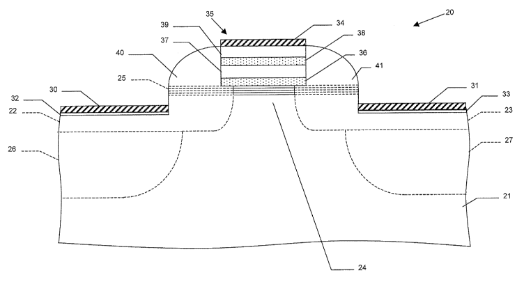
which a plurality of layers, less than eight monolayers, and containing a
fraction or a binary compound semiconductor layers, are alternately and
CA 02650809 2008-10-23
WO 2007/131117 PCT/US2007/068155
epitaxially grown. The direction of main current flow is perpendicular to the
layers of the superlattice.
[0005] U.S. Patent No. 5,357,119 to Wang et al. discloses a Si-Ge short period
superlattice with higher mobility achieved by reducing alloy scattering in the
superlattice. Along these lines, U.S. Patent No. 5,683,934 to Candelaria
discloses an enhanced mobility MOSFET including a channel layer comprising
an alloy of silicon and a second material substitutionally present in the
silicon
lattice at a percentage that places the channel layer under tensile stress.
[0006] U.S. Patent No. 5,216,262 to Tsu discloses a quantum well structure
comprising two barrier regions and a thin epitaxially grown semiconductor
layer sandwiched between the barriers. Each barrier region consists of
alternate layers of Si02/Si with a thickness generally in a range of two to
six
monolayers. A much thicker section of silicon is sandwiched between the
barriers.
[0007]An article entitled "Phenomena in silicon nanostructure devices" also to
Tsu and published online September 6, 2000 by Applied Physics and
Materials Science & Processing, pp. 391-402 discloses a semiconductor-
atomic superlattice (SAS) of silicon and oxygen. The Si/O superlattice is
disclosed as useful in a silicon quantum and light-emitting devices. In
particular, a green electroluminescence diode structure was constructed and
tested. Current flow in the diode structure is vertical, that is,
perpendicular to
the layers of the SAS. The disclosed SAS may include semiconductor layers
separated by adsorbed species such as oxygen atoms, and CO molecules.
The silicon growth beyond the adsorbed monolayer of oxygen is described as
epitaxial with a fairly low defect density. One SAS structure included a 1.1
nm
thick silicon portion that is about eight atomic layers of silicon, and
another
structure had twice this thickness of silicon. An article to Luo et al.
entitled
"Chemical Design of Direct-Gap Light-Emitting Silicon" published in Physical
Review Letters, Vol. 89, No. 7 (August 12, 2002) further discusses the light
emitting SAS structures of Tsu.
2
CA 02650809 2008-10-23
WO 2007/131117 PCT/US2007/068155
[0008] Published International Application WO 02/103,767 Al to Wang, Tsu
and Lofgren, discloses a barrier building block of thin silicon and oxygen,
carbon, nitrogen, phosphorous, antimony, arsenic or hydrogen to thereby
reduce current flowing vertically through the lattice more than four orders of
magnitude. The insulating layer/barrier layer allows for low defect epitaxial
silicon to be deposited next to the insulating layer.
[0009] Published Great Britain Patent Application 2,347,520 to Mears et al.
discloses that principles of Aperiodic Photonic Band-Gap (APBG) structures
may be adapted for electronic bandgap engineering. In particular, the
application discloses that material parameters, for example, the location of
band minima, effective mass, etc, can be tailored to yield new aperiodic
materials with desirable band-structure characteristics. Other parameters,
such as electrical conductivity, thermal conductivity and dielectric
permittivity
or magnetic permeability are disclosed as also possible to be designed into
the material.
[0010] Despite considerable efforts at materials engineering to increase the
mobility of charge carriers in semiconductor devices, there is still a need
for
greater improvements. Greater mobility may increase device speed and/or
reduce device power consumption. With greater mobility, device performance
can also be maintained despite the continued shift to smaller device features.
Summary of the Invention
[0011] In view of the foregoing background, it is therefore an object of the
present invention to provide a semiconductor device including one or more
non-volatile memory cells having relatively high charge carrier mobility.
[0012] This and other objects, features, and advantages in accordance with
the present invention are provided by a semiconductor device including at
least one non-volatile memory cell comprising a superlattice channel. More
particularly, the device may include a semiconductor substrate, the at least
non-volatile memory cell may include spaced apart source and drain regions,
and the superlattice channel may be between the source and drain regions.
The superlattice channel may include a plurality of stacked groups of layers
on
3
CA 02650809 2008-10-23
WO 2007/131117 PCT/US2007/068155
the semiconductor substrate between the source and drain regions. Moreover,
each group of layers of the super[attice channel may include a plurality of
stacked base semiconductor monolayers defining a base semiconductor
portion and an energy band-modifying layer thereon. Also, the energy band-
modifying layer may include at least one non-semiconductor monolayer
constrained within a crystal lattice of adjacent base semiconductor portions.
[0013]The at least one non-volatile memory cell may further include floating
gate adjacent the superiattice channel, and a control gate adjacent the
floating
gate. In one embodiment, the at least one non-volatile memory cell may also
include a first insulating layer (e.g., an oxide layer) between the floating
gate
and the control gate. A second insulating layer may also be between the
superlattice channel and the floating gate. In an alternate embodiment, a
superlattice insulating layer may be between the floating gate and the control
gate to advantageously provide vertical insulation between the floating and
control gates.
[0014] More specifically, the superlattice channel may have a common energy
band structure therein, and it may also have a higher charge carrier mobility
than woufd otherwise be present without the energy band-modifying layer. By
way of example, each base semiconductor portion may comprise at least one
of silicon and germanium, and each energy band-modifying layer may
comprise oxygen. Further, each energy band-modifying layer may be a single
monolayer thick, and each base semiconductor portion may be less than eight
monolayers thick.
[0075] The superlattice may further have a substantially direct energy
bandgap, and it may also include a base semiconductor cap layer on an
uppermost group of layers. In one embodiment, all of the base semiconductor
portions may be a same number of monolayers thick. In accordance with an
alternate embodiment, at least some of the base semiconductor portions may
be a different number of monolayers thick. In addition, each energy band-
modifying layer may include a non-semiconductor selected from the group
consisting of oxygen, nitrogen, fluorine, and carbon-oxygen, for example. A
4
CA 02650809 2008-10-23
WO 2007/131117 PCT/US2007/068155
contact layer may also be included on at least one of the source and drain
regions.
[0016]Another aspect of the invention is directed to a method for making a
semiconductor device including at least one non-volatile memory cell
comprising a superlattice channel. More particularly, the method may include
forming the at least non-volatile memory cell by forming spaced apart source
and drain regions, and forming the superlattice channel between the source
and drain regions. The superlattice channel may include a plurality of stacked
groups of layers on the semiconductor substrate between the source and
drain regions. Moreover, each group of layers of the superlattice channel may
include a plurality of stacked base semiconductor monolayers defining a base
semiconductor portion and an energy band-modifying layer thereon. Also, the
energy band-modifying layer may include at least one non-semiconductor
monolayer constrained within a crystal lattice of adjacent base semiconductor
portions.
[0077] Forming the at least one non-volatile memory cell may further include
forming a floating gate adjacent the superlattice channel, and forming a
control
gate adjacent the floating gate. In one embodiment, a first insulating layer
(e.g., an oxide layer) may be formed between the floating gate and the control
gate. A second insulating layer may also be formed between the superlattice
channel and the floating gate. In an alternate embodiment, a superlattice .
insulating layer may be formed between the floating gate and the control gate
to advantageously provide vertical insulation between the gates.
Brief Description of the Drawin s
[0018] FIG. 1 is schematic cross-sectional view of a semiconductor device
including a non-volatile memory cell with a superlattice channel in accordance
with the present invention.
[0019]FlG. 2 is a schematic cross-sectional view of an alternate embodiment
of the semiconductor device of FIG. 1.
[0020] FIG. 3 is a greatly enlarged schematic cross-sectional view of
the superlattice as shown in FIG. 1,
CA 02650809 2008-10-23
WO 2007/131117 PCT/US2007/068155
[0021] FIG. 4 is a perspective schematic atomic diagram of a portion of
the superlattice shown in FIG. 1.
[0022] FIG. 5 is a greatly enlarged schematic cross-sectional view of
another embodiment of a superiattice that may be used in the device of FIG. .
1 .
[0023] FIG. 6A is a graph of the calculated band structure from the
gamma point {G} for both bulk silicon as in the prior art, and for the 411
Si/O
superlattice as shown in FIGS. 1-3.
[0024] FIG. 6B is a graph of the calculated band structure from the Z
point for both bulk silicon as in the prior art, and for the 4/1 Si/O
superlattice as
shown in FIGS. 1-3.
[0025] FIG. 6C is a graph of the calculated band structure from both the
gamma and Z points for both bulk silicon as in the prior art, and for the
511/3/1
Si/O superlattice as shown in FIG. 4.
[0026] FIGS. 7A-7D are a series of schematic cross-sectional diagrams
illustrating a method for making the semiconductor device of FIG. 1.
Detailed Description of the Preferred Embodiments
[0027]The present invention will now be described more fully hereinafter with
reference to the accompanying drawings, in which preferred embodiments of
the invention are shown. This invention may, however, be embodied in many
different forms and should not be construed as limited to the embodiments set
forth herein. Rather, these embodiments are provided so that this disclosure
will be thorough and complete, and will fully convey the scope of the
invention
to those skilled in the art. Like numbers refer to like elements throughout,
and
prime notation is used to indicate similar elements in alternate embodiments.
[0028] The present invention relates to controlling the properties of
semiconductor materials at the atomic or molecular level to achieve improved
performance within semiconductor devices. Further, the invention relates to
the identification, creation, and use of improved materials for use in the
conduction paths of semiconductor devices.
6
CA 02650809 2008-10-23
WO 2007/131117 PCT/US2007/068155
[00291 Applicants theorize, without wishing to be bound thereto, that
certain superlattices as described herein reduce the effective mass of charge
carriers and that this thereby leads to higher charge carrier mobility.
Effective
mass is described with various. definitions in the literature. As a measure of
the
improvement in effective mass Applicants use a "conductivity reciprocal
effective mass tensor", Mei and Mh' for electrons and holes respectively,
defined as:
c~f(E(k, n), EF , T)
I f (OkE(k,n)); (VkE(k,n)); aE d s k
E> EF B.z.
Melj(EF?T)
, ff(E(k,n),E,,T)d3k
E>Fr B.Z.
for electrons and:
- ~ f ( kE(k,n))j {V,,E(k,n))j Of (E(k9n), E., T ) d'k
) a.z. r~E
Mh;j(E~,~' ~
I f(1- f(E(k,n),EF,T))d'k
.E < EF B.Z.
for holes, where f is the Fermi-Dirac distribution, EF is the Fermi energy, T
is
the temperature, E(k,n) is the energy of an electron in the state
corresponding
to wave vector k and the rtth energy band, the indices i and j refer to
Cartesian
coordinates x, y and z, the integrals are taken over the Brillouin zone
(B.Z.),
and the summations are taken over bands with energies above and below the
Fermi energy for electrons and holes respectively.
[4030] Applicants' definition of the conductivity reciprocal effective mass
tensor is such that a tensorial component of the conductivity of the material
is
greater for greater values of the corresponding component of the conductivity
reciprocal effective mass tensor. Again Applicants theorize without wishing to
be bound thereto that the superlattices described herein set the values of the
7
CA 02650809 2008-10-23
WO 2007/131117 PCT/US2007/068155
conductivity reciprocal effective mass tensor so as to enhance the conductive
properties of the material, such as typically for a preferred direction of
charge
carrier transport. The inverse of the appropriate tensor element is referred
to
as the conductivity effective mass. In other words, to characterize
semiconductor material structures, the conductivity effective mass for
electrons/holes as described above and calculated in the direction of intended
carrier transport is used to distinguish improved materials.
[0031] Using the above-described measures, one can select materials
having improved band structures for specific purposes. One such example
would be a superlattice 25 material for a channel region in a semiconductor
device. A non-volatile memory device 20 including the superfattice 25 in
accordance with the invention is now first described with reference to FIG. 1.
One skilled in the art, however, will appreciate that the materials identified
herein could be used in many different types of semiconductor devices, such
as discrete devices andlor integrated circuits.
[0032] The illustrated memory device 20 includes a non-volatile memory
cell formed on a substrate 21. The memory cell illustratively includes lightly
doped sourceldrain extension regions 22, 23, more heavily doped
source/drain regions 26, 27, and a channel region therebetween provided by
the superiattice 25. Portions of the superlattice 25 which are doped while
forming the lightly doped source/drain extension regions 22, 23 are indicated
with dashes for clarity of illustration, while the undoped portions are
indicated
with solid lines. Source/drain silicide layers 30, 31 and source/drain
contacts
32, 33 overlie the source/drain regions 26, 27, as will be appreciated by
those
skilled in the art.
[0033] A gate structure 35 illustratively includes a first insulating layer
36 adjacent the channel provided by the superlattice 25, and a floating gate
37
on the first insulating layer. The gate structure 35 further includes a second
insulting layer 38 on the floating gate 37, and a control gate 39 on the
second
insulating layer. By way of example, the floating and control gates 37, 39 may
be polysilicon, and the first and second insulating layers 36, 38 may be oxide
8
CA 02650809 2008-10-23
WO 2007/131117 PCT/US2007/068155
layers (i.e., silicon oxide layers). The first and second insulating layers
36, 38
are indicated by stippling in FIG. 1 for clarity of illustration. Sidewall
spacers
40, 41 are also provided in the illustrated memory device 20, as well as a
siiicide layer 34 on the control gate 39, as will be appreciated by
thosesfcilled
in the art.
[00341 In accordance with an alternate embodiment of the memory
device 20" now described with reference to FIG. 2, the first and second
insulating layers 36, 38 described above may be omitted from the gate
structure 35", and the vertically insulating properties of the superlattice
25"
may instead be utilized. That is, in the illustrated example, the floating
gate
37" is formed directly on the superlattice 25' without an intervening
insulating
(i.e., oxide) layer. As will discussed further below, this configuration is
possible
because the superiattice 25" material described herein not only provides
enhanced mobility in the lateral direction (i.e., between the source/drain
regions 26 , 27"), but it also advantageously acts as an insulator to current
flow in the vertical direction.
[0035] Similarly, a second superlattice insulating layer 55" may be
formed between the floating and control gates 37", 39" to provide vertical
insulation therebetween. The superlattice insulating layer 55" may be of a
same configuration as the superlattice 25", or they may be of different
configurations, examples of which will be discussed further below. Of course,
an oxide or other insulating layer may also be used instead of the
super[attice
insulating layer 55" in this configuration, as will be appreciated by those
skilled in the art.
[0036] Applicants have identified improved materials or structures for
the channel region of the memory device 20. More specifically, the Applicants
have identified materials or structures having energy band structures for
which
the appropriate conductivity effective masses for electrons and/or holes are
substantially less than the corresponding values for silicon.
[0037] Referring now additionally to FIGS. 3 and 4, the materials or
structures are in the form of a superlattice 25 whose structure is controlled
at
9
CA 02650809 2008-10-23
WO 2007/131117 PCT/US2007/068155
the atomic or molecular level and may be formed using known techniques of
atomic or molecular layer deposition. The superlattice 25 includes a plurality
of
layer groups 45a-45n arranged in stacked relation, as perhaps best
understood with specific reference to.the...schematic cross-sectional view of
FIG. 3.
[0038] Each group of layers 45a-45n of the superlattice 25 illustratively
includes a plurality of stacked base semiconductor monolayers 46 defining a
respective base semiconductor portion 46a-46n and an energy band-
modifying layer 50 thereon. The energy band-modifying layers 50 are
indicated by stippling in FIG. 3 for clarity of illustration.
[0039] The energy band-modifying layer 50 illustratively includes one
non-semiconductor monolayer constrained within a crystal iattice of adjacent
base semiconductor portions. In other embodiments, more than one such
monolayer may be possible. It should be noted that reference herein to a non-
semiconductor or semiconductor monolayer means that the material used for
the monolayer would be a non-semiconductor or semiconductor if formed in
bulk. That is, a single monolayer of a material, such as semiconductor, may
not necessarily exhibit the same properties that it would if formed in bulk or
in
a relatively thick layer, as will be appreciated by those skilled in the art.
[0040] Applicants theorize without wishing to be bound thereto that
energy band-modifying layers 50 and adjacent base semiconductor portions
46a-46n cause the superlattice 25 to have a lower appropriate conductivity
effective mass for the charge carriers in the parallel layer direction than
would
otherwise be present. Considered another way, this parallel direction is
orthogonal to the stacking direction. The band-modifying layers 50 may also
cause the superlattice 25 to have a common energy band structure.
[0041] It is also theorized that the semiconductor device, such as the
illustrated memory device 20, enjoys a higher charge carrier mobility based
upon the lower conductivity effective mass than would otherwise be present.
In some embodiments, and as a result of the band engineering achieved by
the present invention, the superiattice 25 may further have a substantially
CA 02650809 2008-10-23
WO 2007/131117 PCT/US2007/068155
direct energy bandgap that may be particularly advantageous for opto-
electronic devices, for example, as described in further detail below.
[0042] As will be appreciated by those skilled in the art, the source/drain
regions 22, 23,.26, 27. and gate structure 35 of the memory device 20 may be.
.
considered as regions for causing the transport of charge carriers through the
superiattice in a parallel direction relative to the layers of the stacked
groups
45a-45n. Other such regions are also contemplated by the present invention.
[0043] The superlattice 25 also illustratively includes a cap layer 52 on
an upper layer group 45n. The cap layer 52 may comprise a plurality of base
semiconductor monolayers 46. The cap layer 52 may have between 2 to 100
monolayers of the base semiconductor, and, more preferably between 10 to
50 monolayers. In the embodiment illustrated above in FIG. 2, the floating
gate
37" may be formed by forming the cap layer 52" to a desired thickness and
doping the cap layer to the desired dopant concentration. Similarly, the
control
gate layer may also be formed by appropriately sizing and doping the cap
layer 52" of the superlattice insulating layer 55".
[0044] Each base semiconductor portion 46a-46n may comprise a base
semiconductor selected from the group consisting of Group IV
semiconductors, Group fil V semiconductors, and Group 11-VI semiconductors.
Of course, the term Group IV semiconductors also includes Group IV-IV
semiconductors, as will be appreciated by those skilled in the art. More
particularly, the base semiconductor may comprise at least one of silicon and
germanium, for example.
[0045] Each energy band-modifying layer 50 may comprise a non-
semiconductor selected from the group consisting of oxygen, nitrogen,
fluorine, and carbon-oxygen, for example. The non-semiconductor is also
desirably thermally stable through deposition of a next layer to thereby
facilitate manufacturing. In other embodiments, the non-semiconductor may
be another inorganic or organic element or compound that is compatible with
the given semiconductor processing as will be appreciated by those skilled in
11
CA 02650809 2008-10-23
WO 2007/131117 PCT/US2007/068155
the art. More particularly, the base semiconductor may comprise at least one
of silicon and germanium, for example
[0046] It should be noted that the term monolayer is meant to include a
single atomic layer andalso a single molecular layer. It is also noted that
the
energy band-modifying layer 50 provided by a single monolayer is also meant
to include a monolayer wherein not all of the possible sites are occupied. For
example, with particular reference to the atomic diagram of FIG. 4, a 4/1
repeating structure is illustrated for silicon as the base semiconductor
material,
and oxygen as the energy band-modifying material. Only half of the possible
sites for oxygen are occupied.
[0047] In other embodiments andlor with different materials this one half
occupation would not necessarily be the case as will be appreciated by those
skilled in the art. Indeed it can be seen even in this schematic diagram, that
individual atoms of oxygen in a given monolayer are not precisely aligned
along a flat plane as will also be appreciated by those of skill in the art of
atomic deposition. By way of example, a preferred occupation range is from
about one-eighth to one-half of the possible oxygen sites being full, although
other numbers may be used in certain embodiments.
[0048] Silicon and oxygen are currently widely used in conventional
semiconductor processing, and, hence, manufacturers will be readily able to
use these materials as described herein. Atomic or monolayer deposition is
also now widely used. Accordingly, semiconductor devices incorporating the
superlattice 25 in accordance with the invention may be readily adopted and
implemented, as will be appreciated by those skilled in the art.
[0049] It is theorized without Applicants wishing to be bound thereto,
that for a superiattice, such as the SiIO superlattice, for example, that the
number of silicon monolayers should desirably be seven or less so that the
energy band of the superlattice is common or relatively uniform throughout to
achieve the desired advantages. The 4/1 repeating structure shown in FIGS. 3
and 4, for Si/O has been modeled to indicate an enhanced mobility for
electrons and holes in the X direction. For example, the calculated
conductivity
12
CA 02650809 2008-10-23
WO 2007/131117 PCT/US2007/068155
effective mass for electrons (isotropic for bulk silicon) is 0.26 and for the
4/1
SiO superlattice in the X direction it is 0.12 resulting in a ratio of 0.46.
Similarly, the calculation for holes yields values of 0.36 for bulk silicon
and
0.16 for the 4I1. Si/O superlattice resulting in a ratio of 0.44. .
[0050] While such a directionally preferential feature may be desired in
certain semiconductor devices, other devices may benefit from a more uniform
increase in mobility in any direction parallel to the groups of layers. It may
also
be beneficial to have an increased mobility for both electrons or holes, or
just
one of these types of charge carriers as will be appreciated by those skilled
in
the art.
[0051] The lower conductivity effective mass for the 4/1 Si/O
embodiment of the superlattice 25 may be less than two-thirds the conductivity
effective mass than would otherwise occur, and this applies for both electrons
and holes. Of course, the superlattice 25 may further comprise at least one
type of conductivity dopant therein, as will also be appreciated by those
skilled
in the art.
[0052] Indeed, referring now additionally to FIG. 5, another embodiment
of a superlattice 26' in accordance with the invention having different
properties is now described. In this embodiment, a repeating pattern of
3111511
is illustrated. More particularly, the lowest base semiconductor portion 46a'
has three monolayers, and the second lowest base semiconductor portion
46b' has five monolayers. This pattern repeats throughout the superlattice
25'.
The energy band-modifying layers 50' may each include a single monolayer.
For such a superlattice 25' including SiIO, the enhancement of charge carrier
mobility is independent of orientation in the plane of the layers. Those other
elements of FIG. 5 not specifically mentioned are similar to those discussed
above with reference to FIG. 2 and need no further discussion herein.
[0453] In some device embodiments, all of the base semiconductor
portions of a superlattice may be a same number of monolayers thick. In other
embodiments, at least some of the base semiconductor portions may be a
13
CA 02650809 2008-10-23
WO 2007/131117 PCT/US2007/068155
different number of monolayers thick. In still other embodiments, all of the
base semiconductor portions may be a different number of monolayers thick.
[0054] ln FIGS. 6A-6C, band structures calculated using Density
.. Functional Theory (DFT) are presented. It is well known in the art that DFT
underestimates the absolute value of the bandgap. Hence all bands above the
gap may be shifted by an appropriate "scissors correction." However the
shape of the band is known to be much more reliable. The vertical energy
axes should be interpreted in this light.
[0055] FIG. 6A shows the calculated band structure from the gamma
point (G) for both bulk silicon (represented by continuous lines) and for the
4/1
Si/O superiattice 25 shown in FIG. 1(represented by dotted lines). The
directions refer to the unit cell of the 411 Si/O structure and not to the
conventional unit cell of Si, although the (001) direction in the figure does
correspond to the (001) direction of the conventional unit cell of Si, and,
hence, shows the expected location of the Si conduction band minimum. The
(100) and (010) directions in the figure correspond to the (110) and (-110)
directions of the conventional Si unit cell. Those skilled in the art will
appreciate that the bands of Si on the figure are folded to represent them on
the appropriate reciprocal lattice directions for the 411 Si/O structure.
[0056] It can be seen that the conduction band minimum for the 4/1
Si/O structure is located at the gamma point in contrast to bulk silicon (Si),
whereas the valence band minimum occurs at the edge of the Brillouin zone in
the (001) direction which we refer to as the Z point. One may also note the
greater curvature of the conduction band minimum for the 4/1 Si/O structure
compared to the curvature of the conduction band minimum for Si owing to the
band splitting due to the perturbation introduced by the additional oxygen
layer.
[0057] FIG. 6B shows the calculated band structure from the Z point for
both bulk silicon (continuous lines) and for the 4/1 Si/O superiattice 25
(doffed
lines). This figure illustrates the enhanced curvature of the valence band in
the
(100) direction.
14
CA 02650809 2008-10-23
WO 2007/131117 PCT/US2007/068155
[0058] F1G. 6C shows the calculated band structure from both the
gamma and Z point for both bulk silicon (continuous lines) and for the 5I11311
SiIO structure of the superfattice 25' of FIG. 5(dotfied lines). Due to the
symmetry of the 5/1/3/1 SiIO structure, the calculated band structures in.the
(100) and (010) directions are equivalent. Thus the conductivity effective
mass
and mobility are expected to be isotropic in the plane parallel to the layers,
i.e.
perpendicular to the (001) stacking direction. Note that in the 5/1/3/1 Si/O
example the conduction band minimum and the valence band maximum are
both at or close to the Z point.
(0069] Although increased curvature is an indication of reduced
effective mass, the appropriate comparison and discrimination may be made
via the conductivity reciprocal effective mass tensor calculation. This leads
Applicants to further theorize that the 5/1/3/1 superlattice 25' should be
substantially direct bandgap. As will be understood by those skilled in the
art,
the appropriate matrix element for optical transition is another indicator of
the
distinction between direct and indirect bandgap behavior.
[0060] Referring now additionally to FIGS. 7A-7E, a method for making
the memory device 20 will now be described. The method begins with
providing the silicon substrate 21. By way of exampie, the substrate may be
an eight-inch wafer 21 of lightly doped P-type or N-type single crystal
silicon
with <100> orientation, although other suitable substrates may also be used.
In accordance with the present example, a[ayer of the superlattice 25 material
is then formed across the upper surface of the substrate 21.
[0061] More particularly, the superlattice 25 material is deposited across
the surface of the substrate 21 using atomic layer deposition and the
epitaxial
silicon cap layer 52 is formed, as discussed previously above, and the surface
is planarized to arrive at the structure of FIG. 7A. It should be noted that
in
some embodiments the superlattice 25 material may be selectively deposited
in those regions where channels are to be formed, rather than across the
entire substrate 21, as will be appreciated by those skilled in the art.
Moreover, planarization may not be required in all embodiments.
CA 02650809 2008-10-23
WO 2007/131117 PCT/US2007/068155
[00621 The epitaxial silicon cap layer 52 may have a preferred thickness
to prevent superlattice consumption during gate oxide growth, or any other
subsequent oxidations, while at the same time reducing or minimizing the
thickness of.the..silicon cap layer to reduce any parallel path of conduction
with .
the superlattice. According to the well-known relationship of consuming
approximately 45% of the underlying silicon for a given oxide grown, the
silicon cap layer 52 may be greater than 45% of the grown gate oxide
thickness plus a small incremental amount to account for manufacturing
tolerances known to those skilled in the art. For the present example, and
assuming growth of a 25 angstrom gate, one may use approximately '[ 3-'[ 5
angstroms of silicon cap thickness.
(0063] FIG. 7B depicts the memory device 20 after the first insulating
layer gate oxide 37, the floating gate 37, the second insulating layer 38, and
the gate electrode 36 are formed. More particularly, two gate oxide and
polysilicon deposition steps are performed, followed by patterning and/or
etching to form the gate stack. Polysilicon deposition refers to low-pressure
chemical vapor deposition (LPCVD) of silicon onto an oxide (hence it forms a
po[ycrystaliine material). The step includes doping with P+ or As- to make it
conducting, and the layer may be around 250 nm thick, for example. Sidewall
spacers 40, 41 may then be formed after LDD formation and over the
super[attice 25, as will be appreciated by those skilled in the art.
[0064] In an alternate embodiment, the first gate insulating later 36 may
be omitted, and the superlattice insulating layer 55" may be formed in the
same manner discussed above on the floating gate layer 37 instead of the
second gate insulating layer 38. This provides the alternate gate structure
illustrated in FIG. 2, as will be appreciated by those skilled in the art.
[0065] Portions of the superlattice 25 material and the substrate 21 may
be removed in the source/drain regions, as will be appreciated by those
skilled
in the art. As may be seen, this step also forms an underlying portion 24 of
the
substrate 21 underlying the superlattice 25. The superlattice 25 material may
be etched in a similar fashion to that described above for the gate structure
16
CA 02650809 2008-10-23
WO 2007/131117 PCT/US2007/068155
35. However, it should be noted that with the non-semiconductor present in
the superlattice 25, e.g., oxygen, the superlatfice may still be etched with
an
etchant formulated for silicon or polysilicon unless the oxygen level is high
enough to form Si02 and then it may be more easily etched using an etchant
formulated for oxides rather than silicon. Of course, the appropriate etch for
a
given implementation will vary based upon the structure and materials used
for the superlattice 25 and substrate 21, as will be appreciated by those of
skill
in the art.
[0066] In addition, the patterning step may include performing a
spinning photoresist, baking, exposure to light (i.e., a photolithography
step),
and developing the resist. Usually, the pattern is then transferred to another
layer (oxide or nitride) which acts as an etch mask during the etch step. The
etch step typically is a plasma etch (anisotropic, dry etch) that is material
selective (e.g., etches silicon ten times faster than oxide) and transfers the
lithography pattern into the material of interest.
[0067] Referring to FIG. 7C, lightly doped source and drain ("LDD")
extensions 22, 23 are formed using n-type or p-type LDD implantation,
annealing, and cleaning. An anneal step may be used before or after the LDD
implantation, but depending on the specific process, it may be omitted. The
clean step is a chemical etch to remove metals and organics prior to
depositing an oxide layer.
[0068] lmplantation of the source and drain regions 26, 27 is illustrated
in FIG. 7D. An Si02 layer is deposited and etched back. The appropriate N-
type or p-type ion implantation is used to form the source and drain regions
26, 27. The structure is then annealed and cleaned. Self-aligned silicide
formation may then be performed to form the silicide layers 30, 31, and 34,
and the source/drain contacts 32, 33, are formed to provide the final
semiconductor device 20 illustrated in FIG. 1. The silicide formation is also
known as salicidation. The salicidation process includes metal deposition
(e.g.
Ti), nitrogen annealing, metal etching, and a second annealing.
17
CA 02650809 2008-10-23
WO 2007/131117 PCT/US2007/068155
[00691 The foregoing is, of course, but one example of a process and
device in which the present invention may be used, and those of skill in the
art
will understand its application and use in many other processes and devices.
In other processes and.devices the structures of the present invention may be
formed on a portion of a wafer or across substantially all of a wafer.
Additionally, the use of an atomic layer deposition tool may also not be
needed for forming the superEattice 26 in some embodiments. For example,
the monolayers may be formed using a CVD tool with process conditions
compatible with control of monolayers, as will be appreciated by those skilled
in the art.
[0070] Many modifications and other embodiments of the invention wifl
come to the mind of one skilled in the art having the benefit of the teachings
presented in the foregoing descriptions and the associated drawings.
Therefore, it is understood that the invention is not to be limited to the
specific
embodiments disclosed, and that modifications and embodiments are
intended to be included within the scope of the appended claims.
18