Note: Descriptions are shown in the official language in which they were submitted.
CA 02650855 2008-10-30
WO 2007/133894 PCT/US2007/067169
LOW DIMENSIONAL THERMOELECTRICS FABRICATED BY
SEMICONDUCTOR WAFER ETCHING
TECHNICAL FIELD
The present invention relates generally to heat transfer and power generation
devices,
and more particularly, to solid-state heat transfer devices.
BACKGROUND INFORMATION
Heat transfer devices may be used for a variety of heating/cooling and power
generation/heat recovery systems, such as refrigeration, air conditioning,
electronics
cooling, industrial temperature control, and power generation through waste
heat
recovery. These heat transfer devices are also scalable to meet the thermal
management needs of a particular system and environment. However, existing
heat
transfer devices, such as those relying on refrigeration cycles, are
environmentally
unfriendly, have limited lifetime, and are bulky due to mechanical components
such
as compressors and the use of refrigerants.
In contrast, solid-state heat transfer devices offer certain advantages, such
as, high
reliability, reduced size and weight, reduced noise, low maintenance, and a
more
environmentally friendly device. For example, thermoelectric devices transfer
heat by
flow of charge through pairs of n-type and p-type semiconductor
thermoelements,
forming structures that are connected electrically in series (or parallel) and
thermally
in parallel. However, due to the relatively high cost and low efficiency of
the existing
thermoelectric devices, they are restricted to small scale applications, such
as
automotive seat coolers, generators in satellites and space probes, and for
local heat
management in electronic devices.
At a given operating temperature, the heat transfer efficiency of
thermoelectric
devices can be characterized by the figure-of-merit that depends on the
Seebeck
coefficient, electrical conductivity and the thermal conductivity of the
thermoelectric
materials employed for such devices. Many techniques have been used to
increase the
heat transfer efficiency of the thermoelectric devices through improving the
figure-of-
1
CA 02650855 2008-10-30
WO 2007/133894 PCT/US2007/067169
merit value, many of these focusing on low dimensional thermoelectric
structures.
For example, in some heat transfer devices two-dimensional superlattice
thermoelectric materials have been employed for increasing the power factor
value of
such devices (see, e.g., Hicks et al., "Experimental study of the effect of
quantum-well
structures on the thermoelectric figure of merit," Phys. Rev. B, vol. 53(16),
R10493-
R10496, 1996). Such devices may require deposition of two-dimensional
superlattice
thermoelectric materials through techniques, such as molecular beam epitaxy or
vapor
phase deposition. Other devices have employed one-dimensional nanorod systems
(see United States Patent Application Serial No. 11/138,615, filed 26 May
2005). All
such devices, however, are fabricated using "bottom up" deposition methods.
Accordingly, successful fabrication of such devices will require significant
development of deposition techniques such that they afford sufficient control
of
doping, crystallinity, purity, and other relevant parameters for generating
reliable high
efficiency thermoelectric performance.
Accordingly, there remains a need to provide a thermal transfer device that
has
enhanced efficiency achieved through improved figure-of-merit of the thermal
transfer device, and for methods of making such a device that are economical.
It
would also be advantageous to provide a device that is scalable to meet the
thermal
management needs of a particular system and environment.
BRIEF DESCRIPTION OF THE INVENTION
In some embodiments, the present invention is directed to thermoelectric
devices
comprising nanostructured thermoelectric elements, such nanostructured
thermoelements being formed by an etching of doped semiconductor wafers-many
of which are commercially available. The present invention is also directed to
methods of making and using such thermoelectric devices, as well as to systems
which employ such devices. Such devices and their manufacture are unique in
that
they employ a "top down" approach to the formation of the nanostructured or
low-
dimensional thermoelectric materials used therein, thereby employing materials
prepared by well-documented and established techniques providing device-ready
thickness and device-quality purity.
2
CA 02650855 2008-10-30
WO 2007/133894 PCT/US2007/067169
In some such above-mentioned embodiments, the present invention is directed to
a
thermoelectric device comprising: (a) a first thermally conductive substrate
having a
first patterned electrode disposed thereon; (b) a second thermally conductive
substrate
having a second patterned electrode disposed thereon, wherein the first and
second
thermally conductive substrates are arranged such that the first and second
patterned
electrodes form an electrically continuous circuit; (c) a plurality of
thermoelectric
elements positioned between the first and second patterned electrodes, wherein
the
thermoelectric elements comprise nanostructures, and wherein the
nanostructures are
formed by electrochemically etching semiconducting material; and (d) a joining
material disposed between the plurality of thermoelectric elements and at
least one of
the first and second patterned electrodes.
In some such above-mentioned embodiments, the present invention is directed to
a
method of manufacturing a thermoelectric device, the method comprising the
steps of:
(a) providing a first thermally conductive substrate having a first patterned
electrode
disposed thereon; (b) providing a second thermally conductive substrate having
a
second patterned electrode disposed thereon; (c) establishing a plurality of
thermoelectric elements positioned between the first and second patterned
electrodes,
wherein the thermoelectric elements comprise nanostructures, and wherein the
nanostructures are formed by electrochemically etching semiconducting; and (d)
disposing a joining material between the plurality of thermoelectric elements
and the
first and second patterned electrodes.
The foregoing has outlined rather broadly the features of the present
invention in
order that the detailed description of the invention that follows may be
better
understood. Additional features and advantages of the invention will be
described
hereinafter which form the subject of the claims of the invention.
BRIEF DESCRIPTION OF THE DRAWINGS
For a more complete understanding of the present invention, and the advantages
thereof, reference is now made to the following descriptions taken in
conjunction with
the accompanying drawings, in which:
3
CA 02650855 2008-10-30
WO 2007/133894 PCT/US2007/067169
FIGURE 1 is a diagrammatical illustration of a system having a thermal
transfer
device, in accordance with some embodiments of the present invention;
FIGURE 2 is a diagrammatical illustration of a power generation system having
a
thermal transfer device, in accordance with some embodiments of the present
invention;
FIGURE 3 is a cross-sectional view of a thermal transfer unit, in accordance
with
some embodiments of the present invention;
FIGURE 4 depicts a process by which a doped semiconductor wafer is
electrochemically etched to yield a nanostructured thermoelectric element, in
accordance with some embodiments of the present invention;
FIGURE 5 is a scanning electron microscopy (SEM) image depicting a
nanostructured thermoelectric element comprising a dendritic morphology, in
accordance with some embodiments of the present invention;
FIGURE 6 is a SEM image depicting a nanostructured thermoelectric element
comprising a triangular morphology, in accordance with some embodiments of the
present invention;
FIGURE 7 is a diagrammatical side view illustrating an assembled module of a
thermal transfer device having a plurality of thermal transfer units, in
accordance with
some embodiments of the present invention; and
FIGURE 8 is a perspective view illustrating a module having an array of
thermal
transfer devices, in accordance with some embodiments of the present
invention.
DETAILED DESCRIPTION OF THE INVENTION
In some embodiments, the present invention is directed to thermoelectric
devices
comprising nanostructured thermoelectric elements, such nanostructured
thermoelements being formed by an etching of doped semiconductor wafers. The
present invention is also directed to methods of making and using such
thermoelectric
devices, as well as to systems which employ such devices. Such devices and
their
4
CA 02650855 2008-10-30
WO 2007/133894 PCT/US2007/067169
manufacture are unique in that they employ a "top down" approach to the
formation
of the nanostructured or low-dimensional thermoelectric materials used
therein.
The term "low-dimensional," as used herein, generally refers to structures
having
features that are electronically two-dimensional or one-dimensional, as
defined by
establishment of (few) discrete energy bands in the small dimension(s). The
term
"nanostructured," as it relates to the thermoelements of the present
invention,
incorporates features that are nanoscale in at least one dimension, e.g.,
nanorods or
nanowires, or nanomesh. Typically, such structures are quantum confined,
meaning
that they possess features with sizes below which discrete energy states
occur.
In the following description, specific details are set forth such as specific
quantities,
sizes, etc. so as to provide a thorough understanding of embodiments of the
present
invention. However, it will be obvious to those skilled in the art that the
present
invention may be practiced without such specific details. In many cases,
details
concerning such considerations and the like have been omitted inasmuch as such
details are not necessary to obtain a complete understanding of the present
invention
and are within the skills of persons of ordinary skill in the relevant art.
Referring to the drawings in general, it will be understood that the
illustrations are for
the purpose of describing a particular embodiment of the invention and are not
intended to limit the invention thereto.
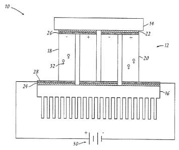
FIGURE 1 illustrates a system 10 having a plurality of thermal transfer
devices in
accordance with certain embodiments of the present invention. As illustrated,
the
system 10 includes a thermal transfer module such as represented by reference
numeral 12, comprised of thermoelectric elements 18 and 20, that transfers
heat from
an area or object 14 to another area or object 16 that may function as a heat
sink for
dissipating the transferred heat. Thermal transfer module 12 may be used for
generating power or to provide heating or cooling of the components. Further,
the
components for generating heat such as object 14 may generate low-grade heat
or
high-grade heat. As will be discussed below, the first and second objects 14
and 16
may be components of a vehicle, or a turbine, or an aircraft engine, or a
solid oxide
CA 02650855 2008-10-30
WO 2007/133894 PCT/US2007/067169
fuel cell, or a refrigeration system. It should be noted that, as used herein
the term
"vehicle" may refer to a land-based, an air-based or a sea-based means of
transportation. In this embodiment, the thermal transfer module 12 includes a
plurality of thermoelectric devices. Note that generally such thermal transfer
modules
comprise at least a pair of such thermoelements; one being an n-type
semiconductor
leg, and the other being a p-type semiconductor leg.
In the above-described embodiment, the thermoelectric module 12 comprises n-
type
semiconductor legs 18 and p-type semiconductor legs 20 that function as
thermoelements, whereby the temperature difference between object 14 and
object 16
produces a voltage difference in the thermoelements in contact with these
objects,
allowing a current to flow, and generating electricity. In this embodiment,
the n-type
and p-type semiconductor legs (thermoelements) 18 and 20 are disposed on
patterned
electrodes 22 and 24 that are coupled to the first and second objects 14 and
16,
respectively. In certain embodiments, the patterned electrodes 22 and 24 may
be
disposed on thermally conductive substrates (not shown) that may be coupled to
the
first and second objects 14 and 16. Further, interface layers 26 and 28 may be
employed to electrically connect pairs of the n-type and p-type semiconductor
legs 18
and 20 on the patterned electrodes 22 and 24.
In the embodiment described above and as depicted in FIGURE 1, the n-type and
p-
type semiconductor legs 18 and 20 are coupled electrically in series and
thermally in
parallel. In certain embodiments, a plurality of pairs of n-type and p-type
semiconductors 18 and 20 may be used to form thermocouples that are connected
electrically in series and thermally in parallel for facilitating the heat
transfer. In
operation, an input voltage source 30 provides a flow of current through the n-
type
and p-type semiconductors 18 and 20. As a result, the positive and negative
charge
carriers transfer heat energy from the first electrode 22 onto the second
electrode 24.
Thus, the thermoelectric module 12 facilitates heat transfer away from the
object 14
towards the object 16 by a flow of charge carriers 32 between the first and
second
electrodes 22 and 24. In certain embodiments, the polarity of the input
voltage source
30 in the system 10 may be reversed to enable the charge carriers to flow from
the
object 16 to the object 14, thus cooling the object 16 and causing the object
14 to
6
CA 02650855 2008-10-30
WO 2007/133894 PCT/US2007/067169
function as a heat sink. As described above, the thermoelectric module 12 may
be
employed for heating or cooling of objects 14 and 16. Further, the
thermoelectric
module 12 may be employed for heating or cooling of objects in a variety of
applications such as air conditioning and refrigeration systems, cooling of
various
components in applications such as an aircraft engine, or a vehicle, or a
turbine and so
forth. In certain embodiments, the thermoelectric device 12 may be employed
for
power generation by maintaining a temperature gradient between the first and
second
objects 14 and 16, respectively that will be described below.
FIGURE 2 illustrates a power generation system 34 having a thermal transfer
device
36 in accordance with aspects of the present invention. The thermal transfer
device
36 includes a p-type leg 38 and an n-type leg 40 configured to generate power
by
maintaining a temperature gradient between a first substrate 42 and a second
substrate
44. In this embodiment, the p-type and n-type legs 38 and 40 are coupled
electrically
in series and thermally in parallel to one another. In operation, heat is
pumped into
the first interface 42, as represented by reference numeral 46 and is emitted
from the
second interface 44 as represented by reference numera148. As a result, an
electrical
voltage 50 proportional to a temperature gradient between the first substrate
42 and
the second substrate 44 is generated due to a Seebeck effect that may be
further
utilized to power a variety of applications that will be described in detail
below.
Examples of such applications include, but are not limited to, use in a
vehicle, a
turbine and an aircraft engine. Additionally, such thermoelectric devices may
be
coupled to photovoltaic or solid oxide fuel cells that generate heat including
low-
grade heat and high-grade heat thereby boosting overall system efficiencies.
It should
be noted that a plurality of thermocouples having the p-type and n-type
thermoelements 38 and 40 may be employed based upon a desired power generation
capacity of the power generation system 34. Further, the plurality of
thermocouples
may be coupled electrically in series, for use in a certain application.
FIGURE 3 illustrates a cross-sectional view of an exemplary configuration 60
of the
thermal transfer device of FIGURES 1 and 2. The thermal transfer device or
unit 60
includes a first thermally conductive substrate 62 having a first patterned
electrode 64
disposed on the first thermally conductive substrate 62. The thermal transfer
device
7
CA 02650855 2008-10-30
WO 2007/133894 PCT/US2007/067169
60 also includes a second thermally conductive substrate 66 having a second
patterned
electrode 68 disposed thereon. In this embodiment, the first and second
thermally
conductive substrates 62 and 66 comprise a thermally conductive and
electrically
insulating ceramic. For example, electrically insulating aluminum nitride or
silicon
carbide ceramic may be used for the first and second thermally conductive
substrates
62 and 66. However, other thermally conductive and electrically insulating
materials
may be employed for the first and second thermally conductive substrates 62
and 66.
In certain embodiments, the patterned electrodes 64 and 68 include a metal
such as
aluminum, copper and so forth. In certain embodiments, the patterned
electrodes may
include highly doped semiconductors. Further, the patterning of the electrodes
64 and
68 on the first and second thermally conductive substrates 62 and 66 may be
achieved
by utilizing techniques such as etching, photoresist patterning, shadow
masking,
lithography, or other standard semiconductor patterning techniques. In a
presently
contemplated configuration, the first and second thermally conductive
substrates 62
and 66 are arranged such that the first and second patterned electrodes 64 and
68 are
parallel and laterally offset to one another so as to form an electrically
continuous
circuit.
Moreover, a plurality of thermoelements (thermoelectric elements) 74 and 76
are
established between the first and second patterned electrodes 64 and 68.
Further,
each of the plurality of thermoelements 74 and 76 is formed of a
thermoelectric
material, wherein the material is a doped semiconductor material, and where
thermoelements 74 are p-doped and thermoelements 76 are n-doped (or vice
versa).
Examples of suitable thermoelectric materials include, but are not limited to,
InP,
InAs, InSb, silicon germanium based alloys, bismuth antimonide based alloys,
lead
telluride based alloys, bismuth telluride based alloys, or other III-V, IV, IV-
VI, and II-
VI semiconductors, or any combinations or alloy combinations thereof having
substantially high thermoelectric figure-of-merit. Additionally suitable
materials
include ternary, quaternary, and higher order compound semiconductors.
The thermal transfer device 60 also includes a joining material 78 disposed
between
the plurality of thermoelements 74 and 76 and the first and second patterned
electrodes 64 and 68 for reducing the electrical and thermal resistance of the
interface.
8
CA 02650855 2008-10-30
WO 2007/133894 PCT/US2007/067169
In certain embodiments, the joining material 78 between the thermoelements 74
and
76 and the first patterned electrode 64 may be different than the joining
material 78
between the thermoelements 74 and 76 and the second patterned electrode 68. In
one
embodiment, the joining material 78 includes silver epoxy. It should be noted
that
other conductive adhesives may be employed as the joining materia178. In
particular,
the joining material 78 is disposed between the substrate 72 and the patterned
electrode 64.
In some other embodiments, the thermoelements 74 and 76 may be bonded to the
patterned electrodes 64 and 68 by diffusion bonding through atomic diffusion
of
materials at the joining interface or other techniques such as wafer fusion
bonding for
semiconductor interfaces. As will be appreciated by one skilled in the art,
diffusion
bonding causes micro-deformation of surface features leading to sufficient
contact on
an atomic scale to cause the two materials to bond. In certain embodiments,
gold may
be employed as an interlayer for the bonding and the diffusion bonds may be
achieved
at relatively low temperatures of about 300 C. In certain other embodiments
indium
or indium alloys may be employed as an interlayer for the bonding at
temperatures of
about 100 C to about 150 C. Further, a typical solvent cleaning step may be
applied
on the surfaces to achieve flat and clean surfaces for applying diffusion
bonding.
Examples of solvents for the cleaning step include acetone, isopropanol,
methanol and
so forth. Further, metal coatings may be disposed on the top and bottom
surfaces of
the thermoelements 74 and 76 and the substrate 72 to facilitate the bonding
between
the thermoelements and the first and second substrates 62 and 66. In one
embodiment, the thermoelements 74 and 76 may be bonded to the patterned
electrodes 64 and 68 through direct diffusion bonding. Alternatively, the
thermoelements 74 and 76 may be bonded to the patterned electrodes 64 and 68
via an
interlayer, such as gold, metal, or solder metal alloy foil. In certain
embodiments, the
bonding between the thermoelements 74 and 76 and the first and second
substrates 62
and 66 may be achieved through an interface layer such as silver epoxy.
However,
other joining methods may be employed to achieve the bonding between the
thermoelements 74 and 76 and the first and second substrates 62 and 66.
9
CA 02650855 2008-10-30
WO 2007/133894 PCT/US2007/067169
In a presently contemplated configuration, the thermoelements 74 and 76
comprise
nanostructured morphologies where quantum confinement effects are dominant.
Typically, this involves nanostructures with dimensions below about 30 nm, and
such
nanostructures are generally formed using an electrochemical etching process.
Further, the electronic density of states of the charge carriers and phonon
transmission
characteristics can be controlled by altering the morphology and composition
of the
thermoelements 74 and 76, thereby enhancing the efficiency of the
thermoelectric
devices that is characterized by the figure-of-merit of the thermoelectric
device. As
used herein, "figure-of-merit" (ZT) refers to a measure of the performance of
a
thermoelectric device and is represented by the equation:
ZT = a 2 T/pKT (1)
where: a is the Seebeck coefficient;
T is the absolute temperature;
p is the electrical resistivity of the thermoelectric material; and
KT is thermal conductivity of the thermoelectric material.
In some embodiments, the thermal transfer device of FIGURES. 1-3 may include
multiple layers, each of the layers having a plurality of thermoelements to
provide
appropriate materials composition and doping concentrations to match the
temperature gradient between the hot and cold sides for achieving maximum
figure-
of-merit (ZT) and efficiency.
In contrast to previous methods for making nanostructured thermoelectric
devices
using a "bottom up" approach to the formation of the nanostructures (see
United
States Patent Application Serial No. 11/138,615, filed 26 May 2005), the
present
invention employs a top down approach. Referring to FIGURE 4, in some
embodiments, an n- or p-doped semiconductor wafer 92 (precursor to
thermoelements
74 and 76) is electrochemically etched to yield a nanostructured material 94
comprising nano- or low-dimensional structures which make the material
suitable for
CA 02650855 2008-10-30
WO 2007/133894 PCT/US2007/067169
use as a thermoelement in a thermoelectric device. As mentioned above, such
nanostructures exhibiting enhanced thermoelectric performance relative to the
corresponding bulk parent material typically comprise features with dimensions
below about 30 nm.
In fabricating such above-mentioned thermoelements, in some embodiments a
doped
wafer of thickness on the order of hundreds of micrometers is chosen, wherein
the
doping densities are chosen for particular thermoelectric performance
(typically, such
doping densities are ca. l0i'-1020 crri 3). The wafer is then etched via
anodization (ca.
a few Volts (V)). Depending on the wafer material and on the anodization
conditions,
the wafer becomes nanostructured upon etching. The nanostructures can be one
of a
variety of morphologies including, but not limited to, dendritic morphology,
triangular morphology, vertical cylindrical pores, nanomesh, and combinations
thereof.
As an example of the above-described thermoelement fabrication, for a (100)-
oriented
n-InP wafer (resistivity of 1.07x10⁻³ ohm-cm; 380-420 ^m thick wafer), using a
sputter-coated TiW/Au as back contact, a triangular morphology was obtained
for
anodization potentials less than 1.6 V vs SCE (saturated calomel electrode as
reference), and the dendritic morphology was observed for potentials greater
than 1.6
V vs SCE. All such exemplary anodizations were conducted in a 1 M HC1
solution,
with or without added nitric acid (3 mL nitric acid in 200 mL 1 M HC1
solution), and
in a manner similar to that described in Fujikura et al., "Electrochemical
Formation of
Uniform and Straight Nano-Pore Arrays on (001) InP Surfaces and Their
Photoluminescence Characteristics," Jpn. J. Appl. Phys., Vol 39, pp. 4616-
4620,
2000. It should be stressed that both morphologies can potentially exhibit
enhanced
thermoelectric performance provided that the size of the nanoscale features
are below
that which discrete energy states occur. FIGURE 5 is a scanning electron
microscopy
(SEM) image depicting a InP nanostructured thermoelectric element comprising a
dendritic morphology, while FIGURE 6 depicts the same having a triangular
morphology. For additional details on anodic etching of InP see Langa et al.,
"Formation of Porous Layers with Different Morphologies During Anodic Etching
of
n-InP," Electrochemical and Solid-State Lett., 3(11), 514-516 (2000).
11
CA 02650855 2008-10-30
WO 2007/133894 PCT/US2007/067169
The nanostructured thermoelectric elements are incorporated as depicted in
FIGURE
3. Specifically, the nanostructured thermoelements are bonded to the patterned
electrodes using a suitable joining material and process (see above).
Variations on the above-described method embodiments include: (a) a second
preparative step involving wet etching of the anodized wafer to create
nanowires or
other nanostructures; (b) a surface passivation step to reduce electronic
defect states;
and (c) filling the void space of the nanostructured wafer 94 with insulating
material
(e.g., polymer) for added mechanical support.
FIGURE 7 illustrates a cross-sectional side view of a thermal transfer device
or an
assembled module 140 having a plurality of thermal transfer devices or thermal
transfer units 60 in accordance with embodiments of the present technique. In
the
illustrated embodiment, the thermal transfer units 60 are mounted between
opposite
substrates 142 and 144 and are electrically coupled to create the assembled
module
140. In this manner, the thermal transfer devices 60 cooperatively provide a
desired
heating or cooling capacity, which can be used to transfer heat from one
object or area
to another, or provide a power generation capacity by absorbing heat from one
surface
at higher temperatures and emitting the absorbed heat to a heat sink at lower
temperatures. In certain embodiments, the plurality of thermal transfer units
60 may
be coupled via a conductive joining material, such as silver filled epoxy or a
metal
alloy. The conductive joining material or the metal alloy for coupling the
plurality of
thermal transfer devices 60 may be selected based upon a desired processing
technique and a desired operating temperature of the thermal transfer device.
Finally,
the assembled module 60 is coupled to an input voltage source via leads 146
and 148.
In operation, the input voltage source provides a flow of current through the
thermal
transfer units 60, thereby creating a flow of charges via the thermoelectric
mechanism
between the substrates 142 and 144. As a result of this flow of charges, the
thermal
transfer devices 60 facilitate heat transfer between the substrates 142 and
144.
Similarly, the thermal transfer devices 60 may be employed for power
generation
and/or heat recovery in different applications by maintaining a thermal
gradient
between the two substrates 142 and 144
12
CA 02650855 2008-10-30
WO 2007/133894 PCT/US2007/067169
FIGURE 8 illustrates a perspective view of a thermal transfer module 150
having an
array of thermal transfer thermoelements 104 in accordance with embodiments of
the
present technique. In this embodiment, the thermal transfer devices 104 are
employed
in a two-dimensional array to meet a thermal management need of an environment
or
application. The thermal transfer devices 104 may be assembled into the heat
transfer
module 150, where the devices 104 are coupled electrically in series and
thermally in
parallel to enable the flow of charges from the first object 14 in the module
150 to the
second object 16 thereby facilitating heat transfer between the first and
second objects
14 and 16 in the module 150. It should be noted that the voltage source 30 may
be a
voltage differential that is applied to achieve heating or cooling of the
first or second
objects 14 and 16. Alternatively, the voltage source 30 may represent an
electrical
voltage generated by the module 150 when used in a power generation
application.
Various aspects of the techniques described above find utility in a variety of
heating/cooling systems, such as refrigeration, air conditioning, electronics
cooling,
industrial temperature control, and so forth. The thermal transfer devices as
described
above may be employed in air conditioners, water coolers, climate controlled
seats,
and refrigeration systems including both household and industrial
refrigeration. For
example, such thermal transfer devices may be employed for cryogenic
refrigeration,
such as for liquefied natural gas (LNG) or superconducting devices. Further,
the
thermal transfer devices as described above may be employed for cooling of
components in various systems, such as, but not limited to vehicles, turbines
and
aircraft engines. For example, a thermal transfer device may be coupled to a
component of an aircraft engine such as, a fan, or a compressor, or a
combustor or a
turbine case. An electric current may be passed through the thermal transfer
device to
create a temperature differential to provide cooling of such components.
Alternatively, the thermal transfer device described herein may utilize a
naturally
occurring or manufactured heat source to generate power. For example, the
thermal
transfer devices described herein may be used in conjunction with geothermal
based
heat sources where the temperature differential between the heat source and
the
ambient (whether it be water, air, etc.) facilitates power generation.
Similarly, in an
aircraft engine the temperature difference between the engine core air flow
stream and
13
CA 02650855 2008-10-30
WO 2007/133894 PCT/US2007/067169
the outside air flow stream results in a temperature differential through the
engine
casing that may be used to generate power. Such power may be used to operate
or
supplement operation of sensors, actuators, or any other power applications
for an
aircraft engine or aircraft. Additional examples of applications within which
thermoelectric devices described herein may be used include gas turbines,
steam
turbines, vehicles, and so forth. Such thermoelectric devices may be coupled
to
photovoltaic or solid oxide fuel cells that generate heat thereby boosting
overall
system efficiencies.
The thermal transfer devices described above may also be employed for thermal
energy conversion and for thermal management. It should be noted that the
materials
and the manufacturing techniques for the thermal transfer device may be
selected
based upon a desired thermal management need of an object. Such devices may be
used for cooling of microelectronic systems such as microprocessor and
integrated
circuits. Further, the thermal transfer devices may be employed for thermal
management of semiconductor devices, photonic devices, and infrared sensors.
A prime advantage of the present invention over existing methods is that, at
least for
some embodiments, the present invention permits the use of semiconductor
wafers of
known electrical, structural and thermal properties, available from wafer
suppliers, as
the starting material for the fabrication, via electrochemical etching, of the
low
dimensional thermoelectric structures described herein. Methods of the present
invention permit the rapid, inexpensive, and reproducible fabrication of low
dimensional thermoelectrics that can be easily integrated into practical
devices.
The following examples are included to demonstrate particular embodiments of
the
present invention. It should be appreciated by those of skill in the art that
the methods
disclosed in the examples that follows merely represent exemplary embodiments
of
the present invention. However, those of skill in the art should, in light of
the present
disclosure, appreciate that many changes can be made in the specific
embodiments
described and still obtain a like or similar result without departing from the
spirit and
scope of the present invention.
14
CA 02650855 2008-10-30
WO 2007/133894 PCT/US2007/067169
EXAMPLE 1
This Example serves to illustrate etching of a semiconductor wafer to form low-
dimensional or nanostructured thermoelectric elements for use in
thermoelectric
devices, in accordance with some embodiments of the present invention.
An InP wafer ((100) orientation, 500 ^m thick, 10i7-l0ig crri 3 doping, n-
type) is
electrically contacted to a Pt back contact. The InP electrode prepared in
this way is
immersed into an aqueous 1 M HC1 electrolyte solution. A 4 mm2 window of the
InP
electrode is exposed for anodization in the dark at room temperature using a 3-
electrode configuration at anode potentials of 1 to 2 V with respect to a
reference
electrode. Depending on the voltage and solution conditions used, anodization
times
providing the appropriate etching depths are used, thereby providing a high
level of
control over the formation of the nanostructures.
EXAMPLE 2
This Example serves to illustrate the incorporation of an etched semiconductor
wafer
into a thermoelectric device, in accordance with some embodiments of the
present
invention.
In constructing a device incorporating the etched wafer of EXAMPLE 1, the
following steps can be taken: (1) The wafer can be etched to > 50% of the
total wafer
thickness, thereby developing the desired morphology over a significant
fraction of
the wafer; (2) In a subsequent step, the void space of the etched structure
may
optionally be filled with insulating material (e.g., polymer) for added
mechanical
support using established techniques (i.e., spin casting the filler from
solution, vapor
deposition processes); (3) The device is then assembled by bonding equal
numbers of
both p- and n-type etched wafers to the metal electrodes of the patterned
thermally-
conductive substrate 62 and 66 in device 60 described above using known
bonding
techniques, as described herein. The p- and n-type etched wafers comprise
CA 02650855 2008-10-30
WO 2007/133894 PCT/US2007/067169
thermoelements of the device, and are arranged in alternating fashion, as
shown in
FIGURES 1 and 3.
It will be understood that certain of the above-described structures,
functions, and
operations of the above-described embodiments are not necessary to practice
the
present invention and are included in the description simply for completeness
of an
exemplary embodiment or embodiments. In addition, it will be understood that
specific structures, functions, and operations set forth in the above-
described
referenced patents and publications can be practiced in conjunction with the
present
invention, but they are not essential to its practice. It is therefore to be
understood
that the invention may be practiced otherwise than as specifically described
without
actually departing from the spirit and scope of the present invention as
defined by the
appended claims.
16