Note: Descriptions are shown in the official language in which they were submitted.
CA 02651000 2008-10-31
WO 2007/130628 PCT/US2007/010927
1
IMPLANTABLE WIRELESS SENSOR FOR IN VIVO PRESSURE
MEASUREMENT AND CONTINUOUS OUTPUT DETERMINATION
TECHNICAL FIELD
[0001] This invention relates to implanted sensors for wirelessly sensing
pressure,
temperature and other physical properties within the human body. More
particularly, the invention
concerns a wireless, un-powered, micromachined pressure sensor that can be
delivered using
catheter-based endovascular or surgical techniques to a location within an
organ or vessel.
BACKGROUND OF THE INVENTION
[0002] The measurement of blood pressure within the hurrian heart and its
vasculature
provides critical information regarding the organ's function. Many methods and
techniques have
been developed to give physicians the ability to monitor heart function to
properly diagnose and
treat various diseases and medical conditions. For example, a sensor placed
within the chambers
of the heart can be used to record variations in blood pressure based on
physical changes to a
mechanical element within the sensor. This information is then transferred
through a wire from
the sensor to an extracorporeal device that is capable of translating the data
from the sensor into a
measurable value that can be displayed. The drawback of this type of sensor is
that there must be
a wired connection between the sensor and the extracorporeal device, thus
limiting its use to acute
settings.
[0003] Many types of wireless sensors have been proposed that would allow
implantation
of the device into the body. Then, through the appropriate coupling means,
pressure reading can
be made over longer periods of interest. The primary limitation to these type
of sensors is that the
fabrication methods used to manufacture them do not provide sufficient
miniaturization to allow
CA 02651000 2008-10-31
WO 2007/130628 PCT/US2007/010927
2
them to be introduced and implanted into the heart using non-surgical,
catheter-based techniques
while maintaining the ability to communicate wirelessly with external
electronics.
[0004] An implantable sensor of this type must be assembled using the
materials and
fabrication methods that ensure appropriate biocompatibility and long term
mechanical and
electrical durability.
[0005] One method of manufacturing a sensor capable of measuring pressure is
to use a
capacitor that is assembled such that one of the capacitive plates will be
displaced with respect to
the other as a result of exposure to externally applied stress. This
displacement will result in a
change in the capacitance that is proportional to the applied stress. Various
patents describe the
fabrication and use of capacitor-based pressure sensors. The primary
limitation of many of these
inventions is that the techniques used to fabricate the sensors do not lend
themselves to the
miniaturization necessary for it to be configured as an implantable medical
device while
maintaining the capability of communicating wirelessly with external
electronics.
[0006] The fabrication methodologies that have been developed in the field of
Micro-
Electro-Mechanical Systems ("MEMS"), however, do specifically provide the
means for
assembling miniaturized sensors capable of measuring a variety of properties
including pressure.
MEMS devices as described in prior patents traditionally use silicon as a
substrate for
construction of miniature electrical or mechanical structures.
[0007] A number of patents detail pressure sensors (some capacitive in nature,
some
manufactured using MEMS based fabrication methods) that are specifically
designed for
implantation into the human body. These sensors suffer from many of the
limitations already
mentioned, with the additional concerns that they require either the addition
of a power source to
operate the device or the need for a physical connection to a device capable
of translating the
sensor output into a meaningful display of a physiologic parameter.
CA 02651000 2008-10-31
WO 2007/130628 PCT/US2007/010927
3
[0008] To overcome the two problems of power and physical connection, the
concept of a
externally modulated LC circuit has been applied to development of implantable
pressure sensors.
Of a number of patents that describe a sensor design of this nature, U.S.
Patent No. 6,113,553 to
Chubbuck is a representative example. The Chubbuck patent demonstrates how a
combination of
a pressure sensitive capacitor placed in series with an inductor coil provides
the basis for a
wireless, un-powered pressure sensor that is suitable for implantation into
the human body.
Construction of an LC circuit in which variations of resonant frequency
correlate to changes in
measured pressure and in which these variations can be detected remotely
through the use of
electromagnetic coupling are further described in U.S. Patent Nos. 6,111,520
and 6,278,379, both
to Allen et al., incorporated herein by reference.
[0009] The device described in the Chubbuck patent is large, thus requiring
surgical
implantation and thereby limiting its applicability to areas that are easily
accessible to surgery
(e.g., the skull).
[0010] Thus, the need exists for a miniature, biocompatible, wireless, un-
powered,
hermetic pressure sensor that can be delivered into the heart or the
vasculature using a small
diameter catheter.
SUMMARY OF THE INVENTION
[0011 ] Stated generally, the present invention comprises a simple apparatus
and method
of monitoring the pressure within the heart or the vasculature by implanting a
pressure sensor in
such locations utilizing catheter-based endovascular or surgical techniques
and using
extracorporeal electronics to measure the pressure easily, safely, and
accurately.
[0012] Stated somewhat more specifically, the present invention is a sensor
having a
capacitive element and a three-dimensional inductor coil connected to said
capacitive element to
CA 02651000 2008-10-31
WO 2007/130628 PCT/US2007/010927
4
form an LC circuit. The LC circuit is hermetically encapsulated within an
electrically insulating
housing. An electrical characteristic of the LC circuit is responsive to a
change in an
environmental parameter.
[0013] Thus it is an object of this invention to provide an implantable
wireless sensor.
[0014] It is also an object of this invention to provide a wireless, passive
micromechanical
sensor that can be delivered endovascularly to a heart charnber or the
vasculature.
[0015] It is a further object of this invention to provide an implantable,
wireless, passive
sensor that can be delivered endovascularly to a heart chamber or the
vasculature to measure
pressure and/or temperature.
[0016] Other objects, features, and advantages of the present invention will
become
apparent upon reading the following specification, when taken in conjunction
with the drawings
and the appended claims.
BRIEF DESCRIPTION OF THE DRAWINGS
[0017] FIG. 1 is a perspective view of a first embodiment of an implantable
wireless
sensor according to the present invention, with the sensor body shown as
transparent to reveal
interior detail.
[0018] FIG. 2 is a schematic view of two pressure sensitive capacitor plates
being formed
in recessed trenches on two substrate wafers.
[0019] FIG. 3 is a schematic view showing the wafers of FIG. 2 imposed in face-
to-face
relation.
[0020] FIG. 4 is a schematic view showing the imposed wafers of FIG. 3 being
laser-cut
around their peripheries.
CA 02651000 2008-10-31
WO 2007/130628 PCT/US2007/010927
[0021] FIG. 5 is a schematic view of an alternate embodiment of two imposed
wafers in
which only one of the wafers has a recessed trench.
[0022] FIG. 6 is a schematic view illustrating a first step in a process for
manufacturing
wafers with capacitor plates formed thereon.
[0023} FIG. 7 is a schematic view illustrating a second step in a process for
manufacturing
wafers with capacitor plates formed thereon.
[0024] FIG. 8 is a schematic view illustrating a third step in a process for
manufacturing
wafers with capacitor plates formed thereon.
[0025] FIG. 9 is a schematic view illustrating a fourth step in a process for
manufacturing
wafers with capacitor plates formed thereon.
[0026] FIG. 10 shows another embodiment in which two capacitor plates are
formed on
one wafer.
[0027] FIG. 11 illustrates the embodiment of FIG. 10 showing the two capacitor
plates on
the single wafer connected to opposite ends of a helical inductor coil.
[0028] FIG. 12 is a schematic view of still another embodiment of an
implantable,
wireless pressure sensor.
[0029] FIG. 13 is a schematic view of a further embodiment of an implantable,
wireless
pressure sensor in which a three-dimensional inductor coil is built onto the
top of through
connection terminals on the backside of a capacitor plate substrate.
[0030] FIG. 14 is a schematic view of another embodiment of a wireless
pressure sensor
in which each subsequent layer is alternately spaced slightly smaller or
larger in diameter than the
previous winding.
[0031] FIG. 15 is a schematic view of a further embodiment of an implantable,
wireless
pressure sensor in which a three-dimensional inductor coil is built onto the
surface of a cylinder.
CA 02651000 2008-10-31
WO 2007/130628 PCT/US2007/010927
6
[0032] FIG. 16 is a schematic view of another embodiment of a wireless
pressure sensor
in which the pressure sensitive capacitor and three-dimensional inductor coil
are formed together
on one wafer.
[0033] FIG. 17 is a schematic view showing a first step in the manufacturing
process of
the wireless pressure sensor of FIG. 16.
[0034] FIG. 18 is a schematic view showing a second step in the manufacturing
process of
the wireless pressure sensor of FIG. 16.
[0035] FIG. 19 is a schematic view showing a third step in the manufacturing
process of
the wireless pressure sensor of FIG. 16.
[0036] FIG. 20 is a schematic view showing a fourth step in the manufacturing
process of
the wireless pressure sensor of FIG. 16.
[0037] FIG. 21 is a schematic view showing a fifth step in the manufacturing
process of
the wireless pressure sensor of FIG. 16.
[0038] FIG. 22 shows a first arrangement for electrically and mechanically
interconnecting a capacitor plate to an inductor coil.
[0039] FIG. 23 shows a second arrangement for electrically and mechanically
interconnecting a capacitor plate to an inductor coil.
[0040] FIG. 24 is a schematic view of another embodiment of a wireless
pressure sensor
in which the pressure sensitive capacitor and three-dimensional inductor coil
are formed on two
wafers.
[0041] FIG. 25 is a schematic view showing a first step in the manufacturing
process of
the wireless pressure sensor of FIG. 24.
[0042] FIG. 26 is a schematic view showing a second step in the manufacturing
process of
the wireless pressure sensor of FIG. 24.
CA 02651000 2008-10-31
WO 2007/130628 PCT/US2007/010927
7
[0043] FIG. 27 is a schematic view showing a third step in the manufacturing
process of
the wireless pressure sensor of FIG. 24.
[0044] FIG. 28 is a schematic view showing a fourth step in the manufacturing
process of
the wireless pressure sensor of FIG. 24.
[0045] FIG. 29 is a schematic view of an embodiment of a wireless pressure
sensor
utilizing four wafers.
[0046] FIG. 30 is a schematic view showing a first step in the manufacturing
process of
the wireless pressure sensor of FIG. 29.
[0047] FIG. 31 is a schematic view showing a second step in the manufacturing
process of
the wireless pressure sensor of FIG. 29.
[0048] FIG. 32 is a schematic view showing a third step in the manufacturing
process of
the wireless pressure sensor of FIG. 29.
[0049] FIG. 33 is a side view of a pressure sensor and a retention mechanism
of a delivery
device, with the retention mechanism in a closed configuration.
[0050] FIG. 34 is a side view of the pressure sensor and retention mechanism
FIG. 33,
with the retention mechanism in an open configuration.
[0051] FIG. 35 is a side view of the pressure sensor and retention mechanism
FIG. 33,
with the retention mechanism in an closed configuration and shown in cross-
section.
[0052] FIG. 36 is a side view of the pressure sensor and retention mechanism
FIG. 33,
with the retention mechanism in an open configuration and shown in cross-
section.
[0053] FIG. 37 is a side view of a dual-coil shaft of a delivery device, with
a portion of
the outer coil being removed to show the inner coil.
CA 02651000 2008-10-31
WO 2007/130628 PCT/US2007/010927
8
[0054] FIG. 38 is a side view of a delivery device comprising the retention
mechanism of
FIG. 33 and the shaft of FIG. 37, illustrating a first step in the delivery of
a sensor into the wall of
a septum.
[0055] FIG. 39 is a side view of the delivery device of FIG. 38, illustrating
a second step
in the delivery of a sensor into the wall of a septum.
[0056] FIG. 40 is a side view of the delivery device of FIG. 38, illustrating
a third step in
the delivery of a sensor into the wall of a septum.
[0057] FIG. 41 is a side view of the delivery device of FIG. 38, illustrating
a fourth step in
the delivery of a sensor into the wall of a septum.
[0058] FIG. 42 is a side view of an alternate embodiment of a delivery device
for
delivering a sensor into the wall of a septum, with the retention mechanism of
the delivery device
in a closed configuration.
[0059] FIG. 43 is a side view of the delivery device of FIG. 42 showing the
retention
mechanism in an open configuration.
[0060] FIG. 44 is an isometric view of a sensor comprising an alternate
arrangement for
anchoring the sensor within a lumen of a patient.
[0061] FIG. 45 is a top view of the sensor of FIG. 44.
[0062] FIG. 46 is a top view showing the sensor of FIG. 44 lodged within a
lumen.
[0063] FIG. 47 is a side cutaway view of a shaft of a delivery apparatus for
implanting the
sensor of FIG. 44.
[0064] FIG. 48 is a side view of a tether wire of a delivery apparatus for
implanting the
sensor of FIG. 44.
[0065] FIG. 49 is a side view of a core wire of a delivery apparatus for
implanting the
sensor of FIG. 44.
CA 02651000 2008-10-31
WO 2007/130628 PCT/US2007/010927
9
[0066] FIG. 50 is a side view of a guidewire of a delivery apparatus for
implanting the
sensor of FIG. 44.
[0067] FIG. 51 is a side cutaway view of a delivery apparatus comprising the
components
of FIGS. 47-50 with the sensor of FIG. 44 mounted thereto.
DETAILED DESCRIPTION OF THE DISCLOSED EMBODIMENT
[0068] Referring now to the drawings, in which like numerals indicate like
elements
throughout the several views, FIG. 1 illustrates a sensor 10 for the
measurement of physical
parameters. The sensor can be fabricated using micro-machining techniques and
is small,
accurate, precise, durable, robust, biocompatible, and insensitive to changes
in body chemistry, or
biology. Additionally, the sensor can incorporate radiopaque features to
enable fluoroscopic
visualization during placement within the body. Furthermore, this sensor is
encased in a
hermetic, unitary package of electrically insulating material where the
package is thinned in one
region so as to deform under a physiologically relevant range of pressure. The
LC circuit
contained in the packaging is configured so that one electrode of the
capacitor is formed on the
thinned region. This sensor does not require the use of extemal connections to
relay pressure
information externally and does not need an internal power supply to perform
its function. The
pressure sensor of the current invention can be attached to the end of a
catheter to be introduced
into a human body and delivered to an organ or vessel using catheter-based
endovascular
techniques. ,
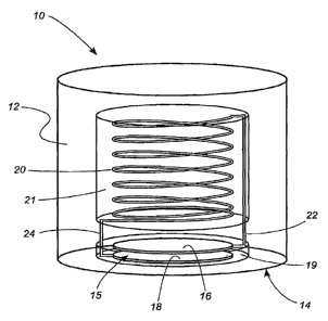
[0069] Referring to FIG. 1, the sensor 10 includes a body 12. The body 12 is
formed from
electrically insulating materials, preferably biocompatible ceramics. In a
preferred embodiment,
the body is comprised of fused silica. The sensor 10 comprises a deflectable
region 14 at the
CA 02651000 2008-10-31
WO 2007/130628 PCT/US2007/010927
lower end of the body 12. The body 12 further comprises a lower chamber 19 and
an upper
chamber 21.
[0070] An LC resonator is hermetically housed within the body 12 and comprises
a
capacitor 15 and an inductor 20. As used herein, the term " hermetic" will be
understood to mean
"completely sealed, especially against the escape or entry of air and bodily
fluids." The capacitor
is located within the lower cylindrical chamber 19 and comprises at least two
plates 16, 18
disposed in parallel, spaced apart relation. The inductor 20 comprises a coil
disposed within the
upper chamber 21 and which is in conductive electrical contact with the
capacitor 15.
[0071] The lower capacitor plate 18 is positioned on the inner surface of the
deflectable
region 14 of the sensor body 12. The upper capacitor plate 16 is positioned on
a fixed region of
the sensor body 12. A change in ambient pressure at the deflectable region 14
of the sensor 10
causes the deflectable region 14 to bend, thereby displacing the lower plate
16 with respect to the
upper plate 18 and changing the capacitance of the LC circuit. Because the
change in capacitance
of the LC circuit changes its resonant frequency, the resonant frequency of
the sensor 10 is
pressure-dependent.
[0072] Beyond what has been presented in U.S. Patent Nos. 6,111,520 and
6,278,379,
covering the fundamental operating principle of the wireless pressure sensor,
additional means to
further sensor miniaturization is required in order to achieve an acceptable
size for implantation
into the heart or the vasculature. The sensor outer dimensions are constrained
by the lumen size of
the delivery catheter that is used to introduce the sensor. Catheter inner
diameters typically range
from 1-5 mm. Also, the size and shape of the sensor should minimally interfere
with mechanical
or hemodynamic function of the heart or vessel where it is located.
[0073] Within these physical size constraints, one of the most significant
challenges is
achieving adequate coupling to the sensor inductor coil from the external
readout device at the
CA 02651000 2008-10-31
WO 2007/130628 PCT/US2007/010927
11
necessary distance from the outside of the body to the implant site. One
method for achieving
enhanced coupling is to add magnetic material to the inductor. However, this
approach is not
feasible in a sensor intended for in vivo use, as the magnetic material would
be adverse to
magnetic resonance imaging, for example. For a limited coil cross-sectional
area, an increased
coupling coefficient is also achievable by using a three-dimensional inductor
coil configuration,
as opposed to two-dimensional designs. For these reasons, a three-dimensional
helical inductor
coil configuration 20 is the preferred embodiment for the sensor design.
LC Circuit Introduction
[0074] The disclosed sensor features a completely passive inductive-capacitive
(LC)
resonant circuit with a pressure varying capacitor. Because the sensor is
fabricated using
completely passive electrical components and has no active circuitry, it does
not require on-board
power sources such as batteries, nor does it require leads to connect to
external circuitry or power
sources. These features create a sensor which is self-contained within the
packaging material and
lacks physical interconnections traversing the hermetic packaging, such
interconnects frequently
being cited for failure of hermeticity. Furthermore, other sensing
capabilities, such as
temperature sensing, can be added using the same manufacturing techniques. For
example,
temperature sensing capability can be accomplished by, the addition of a
resistor with known
temperature characteristics to the basic LC circuit.
[0075] The capacitor in the pressure sensor of the disclosed invention
consists of at least
two conductive elements separated by a gap. If a force is exerted on the
sensor, a portion of the
sensor deflects, changing the relative position between the two conductive
elements. This
movement will have the effect of reducing the gap between the conductive
elements, which will
consequently change the capacitance of the LC circuit. An LC circuit is a
closed loop system
CA 02651000 2008-10-31
WO 2007/130628 PCT/US2007/010927
12
whose resonance is proportional to the inverse square root of the product of
the inductor and
capacitor. Thus, changes in pressure alter the capacitance and, ultimately,
cause a shift in the
resonant frequency of the sensor. The pressure of the environment external to
the sensor is then
determined by referencing the value obtained for the resonant frequency to a
previously generated
curve relating resonant frequency to pressure.
[0076] Because of the presence of the inductor, it is possible to couple to
the sensor
electromagnetically and to induce a current in the LC circuit via a magnetic
loop. This
characteristic allows for wireless exchange of electromagnetic energy with the
sensor and the
ability to operate it without the need for an on-board energy source such as a
battery. Thus it is
possible to determine the pressure surrounding the sensor by a simple, non-
invasive procedure by
remotely interrogating the sensor, recording the resonant frequency, and
converting this value to a
pressure measurement.
[0077] One method of sensor interrogation is explained in U.S. Patent
Application Serial
No. 11/105,294, incorporated herein by reference. According to this invention,
the interrogating
system energizes the sensor with a low duty cycle, gated burst of RF energy
having a
predetermined frequency or set of frequencies and a predetermined amplitude.
The energizing
signal is coupled to the sensor via a magnetic loop. The energizing signal
induces a current in the
sensor that is maximized when the frequency of the energizing signal is
substantially the same as
the resonant frequency of the sensor. The system receives the ring down
response of the sensor
via magnetic coupling and determines the resonant frequency of the sensor,
which is then used to
determine the measured physical parameter. The resonant frequency of the
sensor is determined
by adjusting the frequency of the energizing signal until the phase of the
ring down signal and the
phase of a reference signal are equal or at a constant offset. In this manner,
the energizing signal
CA 02651000 2008-10-31
WO 2007/130628 PCT/US2007/010927
13
frequency is locked to the sensor's resonant frequency and the resonant
frequency of the sensor is
known. The pressure of the localized environment can then be ascertained.
Q-factor and packaging
[0078] Q factor (Q) is the ratio of energy stored versus energy dissipated.
The reason Q is
important is that the ring down rate of the sensor is directly related to the
Q. If the Q is too small,
the ring down rate occurs over a substantially shorter time interval. This
necessitates faster
sampling intervals, making sensor detection more difficult. Also, as the Q of
the sensor increases,
so does the amount of energy returned to external electronics. Thus, it is
important to design
sensors with values of Q sufficiently high enough to avoid unnecessary
increases in complexity in
communicating with the sensor via external electronics.
[0079] The Q of the sensor is dependent on multiple factors such as the shape,
size,
diameter, number of turns, spacing between the turns and cross-sectional area
of the inductor
component. In addition Q will be affected by the materials used to construct
the sensors.
Specifically, materials with low loss tangents will provide a sensor with
higher Q factors.
[0080] The body of the implantable sensor of the disclosed embodiment of the
present
invention is preferably constructed of ceramics such as, but not limited to,
fused silica, quartz,
pyrex and sintered zirconia, that provide the required biocompatibility,
hermeticity and processing
capabilities. These materials are considered dielectrics, that is, they are
poor conductors of
electricity but are efficient supporters of electrostatic or
electroquasistatic fields. An important
property of dielectric materials is their ability to support such fields while
dissipating minimal
energy. The lower the dielectric loss, the lower the proportion of energy
lost, and the more
effective the dielectric material is in maintaining high Q.
CA 02651000 2008-10-31
WO 2007/130628 PCT/US2007/010927
14
[0081] With regard to operation within the human body, there is a second
important issue
related to Q, namely that blood and body fluids are conductive mediums and are
thus particularly
lossy. As a consequence, when a sensor is inunersed in a conductive fluid,
energy from the sensor
will dissipate, substantially lowering the Q and reducing the sensor-to-
electronics distance. It has
been found that such loss can be minimized by further separation of the sensor
from the
conductive liquid. This can be accomplished, for example, by coating the
sensor in a suitable low-
loss-tangent dielectric material. The potential coating material must also
meet stringent
biocompatibility requirements and be sufficiently compliant to allow
transmission of fluid
pressure to the pressure-sensitive deflective region. One preferred material
for this application is
silicone rubber. It should be appreciated that use of a coating is an optional
feature and is not
required to practice the invention per se but such coatings will preserve the
Q of the sensor which
can prove advantageous depending on the intracorporeal location of the sensor.
[0082] There are various manufacturing techniques that can be employed to
realize
sensors according to the current invention. Capacitors and inductors made by a
variety of
methods can be manufactured separately, joined through interconnect methods
and encapsulated
in hermetic packaging. In one embodiment, the pressure sensitive capacitor 15
and the three-
dimensional inductor coil 20 are formed separately and joined together to form
the LC circuit. In
another embodiment, the capacitor and inductor coil can be manufactured
integral with one
another. Additionally, there are several methods to create these discrete
elements and to join each
discrete element to create the final sensor. The following examples are
provided to illustrate
important design considerations and alternative methods for creating these
discrete sensor
elements but should not be construed as limiting the invention in any way.
CA 02651000 2008-10-31
WO 2007/130628 PCT/US2007/010927
Coil description:
[0083] Referring to FIG. 12, the inductor coil 320 is comprised of the
inductor coil body
322 and the coil leads 324. Numerous parameters of the inductor coil can be
varied to optimize
the balance of size and the electrical properties of the circuit, including
the materials, coil
diameter, wire gage, number of coil windings, and cross-sectional area of the
coil body. The
material of the coil must be highly conductive and also biocompatible.
Suitable materials include,
but are not limited to, gold, copper and alloys thereof. If the wire is
sufficiently strong, the coil
can be self-supporting, also known as an "air core" configuration. A solenoid
coil is another
suitable configuration. If the wire is not sufficiently strong unsupported to
maintain its intended
configuration during assembly and in use, the coil can be formed around a
central bobbin
comprised of a suitable dielectric material. In the alternative, the coil can
be encased in a liquid
polymer that can cure or otherwise harden after it is applied to the coil
body. Polyimide is one
preferred material for this application because of its thermal, electrical,
and mechanical
properties. However, processes achieving substantially similar results that
involve lower
processing temperatures would make other polymer choices desirable, such
choices being obvious
to one skilled in the art.
[0084] The wire from which the coil is formed can be solid wire, bundled wire
or cable,
or individually insulated stranded wire.
[0085] The wire gage, coil diameter, cross-sectional area of the coil body,
and number of
windings all influence the value of inductance and the detection range of the
circuit. As any of
these properties increase, so do the size and the inductance of the coil, as
well as the sensor-to-
electronics distance. To specify an inductor coil for use in the sensor, size
considerations must be
balanced with those of inductance and Q.
CA 02651000 2008-10-31
WO 2007/130628 PCT/US2007/010927
16
[0086] A small scale three-dimensional inductor coil can be formed in a
variety of ways.
It can be created conventionally. One such method is machine coil winding of
small diameter
insulated magnet wire, as showri in FIG. 1.
[0087] In another embodiment, shown in FIG. 13, a three-dimensional inductor
coil 420 is
built onto the top of one of the through connections terminals 480 on the
backside of the capacitor
plate substrate 442, using integrated circuit processing techniques and a
multitude of layers. This
coil 420 can be defined and supported by photo-definable dielectric material
such as photo-
defmable polyimide. In the disclosed embodiment, the coil is free standing in
air, supported by
same-material mechanical elements that are strategically positioned to
minimize the effect of the
supporting mechanical elements on the electrical function of the coil.
[0088] In this approach it is desirable to minimize the number of design
layers to improve
batch process yield and to reduce processing time. In a conventional
configuration, such as that
shown in FIG. 13, a spacing layer is required between each winding, making the
number of layers
required equal to two times the number of windings. In one version 500 of the
three-dimensional
coil design, an example of which is shown in FIG. 14, each subsequent coil 510
is alternately
spaced slightly smaller or larger in diameter than the previous winding. This
configuration creates
a small separation between adjacent coils 510 in the x-y plane, eliminating
the need for an extra
vertical spacing layer in between windings. This configuration results in a
number of coil
windings equal to the number of layers, which is more practical for
manufacturing using a MEMS
approach.
[0089] In yet another embodiment 550, shown in FIG. 15, a three-dimensional
inductor
coil 555 is built onto the surface of a cylinder 560 of an appropriate
material such as, but not
limited to fused silica. A conductive layer is first applied to the surface of
the cylinder 560. Then
a mold is formed onto the surface so that parts of the underlying conductive
surface are exposed
CA 02651000 2008-10-31
WO 2007/130628 PCT/US2007/010927
17
and some are covered. A metal may then be formed onto the exposed areas by
electroplating,
sputtering or vapor deposition. The exposed area forms a helical trench that
extends along the
surface of the cylinder, thus realizing an inductor coil.
Capacitor description
[0090] Referring now to FIG. 2, the pressure sensitive capacitor plates 16, 18
are formed
on two separate substrate wafers 40, 42 in recessed trenches 44. At least one
of the wafers 40 has
a substrate thickness in the region 46 of the capacitive plate 16 such that
sufficient plate
deflection occurs due to external pressure change, resulting in a sufficient
change in resonant
frequency per unit pressure (mm Hg) once the LC circuit has been created. If
necessary, the
thickness of the wafer 40 in the region 46 can be reduced by suitable chemical
or mechanical
means, as indicated by the dashed line 47, to provide the desired range of
deflection.
[0091 ] As shown in FIG. 3, the wafers 40, 42 are bonded together such that
the capacitive
plates are 16, 18 parallel and separated by a gap on the order of 0.1-10
microns, preferably 0.1-2
microns.
[0092] The performances of the sensor, especially the propensity of its
capacitance and, in
turn, its resonant frequency to change as a response to an environmental
pressure change, are
closely related to few fundamental geometrical considerations. Widening or
elongating the
deflective region will augment its mechanical flexibility, and, in turn, the
pressure sensitivity of
the sensor. Decreasing the thickness of the deflective area will result in
similar improvements.
However, thinner deflective region can become too fragile or otherwise more
sensitive to
systemic response from the host-organism other than changes in mean and
pulsatile blood
pressure (ex: hyperplasia, tissue overgrowth, etc.). Reducing the gap, while
maintaining adequate
deflective region thickness, offers a complementary alternative to
insufficiently low sensitivity.
CA 02651000 2008-10-31
WO 2007/130628 PCT/US2007/010927
18
As the initial value of the gap is shrinking, the motion of the deflective
region relative to the
initial gap becomes proportionally more important. This results in a greater
change in capacitance
for a given stimulus, therefore enhancing the pressure sensitivity. While
relevant sensitivity can
be achieved with initial air-gap ranging from .1 to 10 micrometers, initial
air-gaps ranging from a
.1 to 2 micrometers are preferable.
[0093] To insure adequate pressure range, the value of the maximum deflection
under
maximum load (indexed, for exampled, on physiologically relevant maximum
pulsatile blood
pressure values, at relevant location in the host-organism) ought to be, in
theory, inferior or equal
to the value of the initial gap. In practice, limiting the maximum deflection
under maximum load
to represent only a fraction of the initial gap (ex: .6 micrometer for a 1
micrometer initial gap)
will ease the fabrication constraints and result in a more robust and
versatile sensor.
[0094] One suitable method for creating the pressure sensitive capacitor is by
electroplating the individual plates 16, 18 in the recessed trenches 44 on a
substrate wafer 40, 42
to a given height H1, H2 that is less than or equal to the depth D1, D2 of the
respective trench 44.
When the wafers are bonded together the capacitive plates are generally
separated by the
difference between the sum of the trench depths and the sum of the plate
heights, (Dl + D2) -
(H 1+ H2). An inherent variation in the height of the plates and the required
range of deflection
for the full operating pressure range are parameters which determine the
initial separation distance
(a.k.a. the gap).
[0095] FIG. 4 illustrates the assembled wafers and capacitor plates laser-cut
around their
peripheries 48, reducing the capacitor to its final size and hermetically
fusing the two wafers
together at 50. A C02 laser can be used at a peak wavelength of about 10
microns if the substrate
is fused silica. Power must be sufficiently large to cut and fuse the wafers
together, while at the
CA 02651000 2008-10-31
WO 2007/130628 PCT/US2007/010927
19
same time being sufficiently small that the internal components of the sensor
are not damaged by
excessive heat.
[0096] In an alternate method, the wafers are pre-bonded using glass frit to
produce a
hermetic seal around the cavities. In this method, the laser cut only releases
the sensors from the
wafer, and does not provide the primary means of creating the hermetic seal.
Other suitable
methods of hermetically sealing the wafers include, but are not limited to,
adhesives, gold
compression bonding, direct laser bonding, and anodic bonding.
[0097] In an alternate embodiment illustrated in FIG. 5, one plate 18 is
formed on a
substrate wafer 142 having a trench 144 with a depth greater that of the
trench 44 in the substrate
wafer 40. The other plate 16 is formed on the inner surface of a wafer 140
without a trench. When
imposed in face-to-face relation, the plate 16 is received into the lower end
of the trench 144 with
the plates 16, 18 disposed in parallel, spaced-apart relation.
[0098] To achieve smaller gap separation distances on the order of 0.1-2
microns, revised
processing methods are employed to bring additional control to the variation
in height across the
conductive plates 16, 18. One method is as follows: the conductive plate 16,
18 is built to a target
height that slightly exceeds the depth of the recess trench 44, as shown in
FIG. 6. In the disclosed
embodiment the plates are formed by electroplating. Preferred materials for
the plates are copper,
gold, and alloys thereof. After building the plates, each conductive plate 16,
18 is polished using
chemical/mecha.nical polishing (CMP) to planarize and reduce the height of the
plate until it is
less than the depth of the trench by the desired amount, as shown in FIG. 9.
[0099] Another method also begins with the plates 16, 18 formed to a height
that slightly
exceeds the depth of the trenches 44, as shown in FIG. 6. The metal capacitor
plates 16, 18 are
mechanically polished to planarize the metal surface down to the surface of
the substrate 40, 42,
as shown in FIG. 7. Following this step, the metal plates are chemically
etched by a selective
CA 02651000 2008-10-31
WO 2007/130628 PCT/US2007/010927
etchant to the height indicated by the dashed line 56 in FIG. 8 to achieve the
desired difference in
height between the height of the plate 16, 18 and the depth of the trench 44,
as shown in FIG. 9.
[0100] Still another method for forming the plates is physical vapor
deposition (PVD),
also known as thin film deposition, in conjunction with photolithography. PVD
is used to deposit
a uniform layer of metal, sub-micrometer to tens of micrometers thick, on a
wafer. Subsequently a
layer of photoresist is deposited, a mask is used to pattern the photoresist,
and a selective etching
technique is utilized to etch away the extra metal and to define the desired
pattern. Other
methods of defining the metal pattern can be utilized, such as shadowmasking,
a method well
known in the art.
[0101] In one approach, shown in FIGS. 10 and 11, a pressure sensitive
capacitor 215 can
be formed by separating the bottom conductive pad into two separate regions
218A, 218B that
capacitively couple to one another via a common third conductive region 216 on
the pressure
sensitive deflective region. The inductor coil 20 is then electrically
connected as shown in FIG.
11, one lead 22 of the coil 20 to the first region 218A, and the other lead 24
of the coil 20 to the
second region 218B.
[0102] When the split-plate design is employed for one side of the capacitor,
as shown in
FIG. 11, the split plates 218A, 218B are preferably located on the fixed side
of the capacitor (i.e.,
opposite the pressure-sensitive side), because the electrical/mechanical
interconnects made to the
split plates in order to complete the LC circuit are less prone to mechanical
failure when the
surface to which they are mechanically attached does not deflect or move
repetitively.
[0103] In yet another embodiment, shown in FIG. 12, the plate on the top wafer
42 is
separated by a dielectric into two conductive regions 318A, 318B, with one
region 318B
substantially larger than the other 318A. After bonding together of the two
wafers 40, 42, the
smaller conductive region 318A is electrically connected to the outer edge of
the pressure
CA 02651000 2008-10-31
WO 2007/130628 PCT/US2007/010927
21
sensitive plate 316, spanning the air gap with a laser weld that is performed
through the substrate
material. The laser wavelength is selected so that it is passes through the
substrate material with
minimal energy absorption, but heats the conductive plate sufficiently to
produce the weld
connection between the top and bottom plates 316, 318A.
Interconnects and methods
[0104] It will be appreciated that sensors embodied by the current invention
can have
capacitive and inductive elements maintained in separate hermetic cavities or
that these elements
may be contained in a single hermetic cavity.
[0105] In one embodiment, the pressure sensitive capacitor 15 needs to be
connected to
the three-dimensional inductor coil 20 while maintaining a hermetic seal
around the internal
cavity that defines the separation gap between the capacitive plates 16, 18.
This can be achieved
by using a variety of through-wafer interconnection methods, familiar to those
skilled in the art.
Referring to FIG. 22, through holes or vias 660 are formed in an upper wafer
662 to provide
mechanical and electrical access to a pair of upper capacitor plates 664, 666.
The wafer through-
holes can be formed before or after plate formation using some combination of
the following
techniques: laser drilling, chemical (wet) etching, conventional or ultrasonic
machining, or dry
etching. As shown in FIG. 22, the vias 660 can optionally be filled with gold,
copper, or other
suitable conductive material to form through-wafer interconnects 668 in
conductive
conununication with the capacitor plates 664, 666. The through-wafer
interconnects 668 thus
form a hermetic seal. Leads from an inductor coil (not shown) are attached to
the through-wafer
interconnects 668 to place the leads in conductive communication with the
capacitor plates 664,
666.
CA 02651000 2008-10-31
WO 2007/130628 PCT/US2007/010927
22
[0106] Referring to FIG. 23, through holes or vias 680 are formed in an upper
wafer 682
to provide mechanical and electrical access to a pair of lower capacitor
plates 684, 686. Electrical
connections to the lower capacitor plates 684, 686 will be accomplished
through leads of the
inductor coil (not shown) or through wires or other suitable conductive means.
[0107] Thermosonic or ultrasonic bonding can be used to connect the inductor
coil to
either an electrode of a capacitor or a through-wafer interconnect.
Thermosonic and ultrasonic
bonding are types of wire bonding used for metal wires including, but not
limited to, gold wires.
Typical temperatures required for thermosonic bonding are between 125-220 C.,
and bonding
occurs when a combination of static and ultrasonic mechanical and thermal
energy is delivered to
the metallic coil wire to be bonded to a metal surface. Ultrasonic bonding is
performed just as
thermosonic bonding but without the use of heat. Useful materials for the
metallized bond sites
and coil comprise gold, copper and aluminum and alloys thereof. Bonds can be
formed between
certain dissimilar metals as well as between all like metals, and such
combinations are widely
known in the art.
[0108] If the metal or metal alloy used for the coil has a dielectric (e.g.,
polymer) coating,
the coating must be removed prior to bonding. The coating can be removed to
expose the metal at
the adhesion point so that bonding can occur by either mechanical or chemical
means.
Alternatively, the parameters (e.g. time, heat, pressure) of the thermosonic
bonding process can
be altered and the geometry of the bonding tool modified so that reliable
mechanical and
electrical interconnects are created. Such modifications cause the coating
material to be pushed
aside, exposing the metal at the bonding site and extruding the wire slightly.
This latter technique
provides certain advantages because it reduces the number of manufacturing
steps.
[0109] An alternate method of conductively connecting the coil to the
capacitive plates is
the solder bump. Solder is applied to the metal-metal interface of the coil
and electrode or
CA 02651000 2008-10-31
WO 2007/130628 PCT/US2007/010927
23
interconnect to form a mechanical and electrical connection. This method can
be used for
capacitor plate or through-wafer interconnections. Lead-free solder should be
used for
biocompatibility. Connection can also be achieved through IC processing
techniques, which allow
for plates and coils to be formed in electrical contact with one another.
Finally laser welds, as
previously discussed, can be used to achieve electrical/mechanical
interconnects.
Example 1
[0110] FIG. 16 illustrates a surface micromachined, capacitor coupled sensor
600. The
capacitor structure 602 comprises at least two plates 604, 606, at least one
604 of which is built
directly atop a first wafer 608. This plate 604 will be referred to as the
bottom plate. The region of
the wafer 608 where the bottom plate 604 is built will be referred to as the
deflective region 610.
If necessary, the thickness of the wafer 608 in the region of the deflective
region 610 can be
reduced in thickness to enhance its deformability.
[0111] The other plate 606 is suspended above the bottom plate 604. The top
plate 606 is
mechanically anchored to the deflective region by pillar-like supporting
elements 612 located at
the periphery of the bottom plate 604. Bottom and top plates 604, 606 are
electrically insulated
and physically separated from one another by an air gap 614. The top electrode
606 mechanical
design, material and dimensions are carefully chosen so that the suspended
part of the electrode
does not structurally deform under its own weight or creep over time.
[0112] A coil 616 of relevant geometry and inductance value is built or
assembled using,
as an example, any of the methods described herein. Its terminals are
electrically and
mechanically connected to either one of the opposite plates 604, 606 of the
capacitor 602. A
capsule 618 or other form of hermetic surrounding is used to encapsulate both
the coil 616 and
capacitor 602.
CA 02651000 2008-10-31
WO 2007/130628 PCT/US2007/010927
24
[0113] To achieve the desired pair of fixed and suspended plates 604, 606, the
fabrication
process of the disclosed embodiment employs a technique known in the art as
"sacrificial layer."
A sacrificial layer is a structural layer that remains buried throughout the
fabrication process
under various layers of material until it can be removed, releasing the
structures and layers built
on top of the sacrificial layer. Once removed, a void remains in place of the
sacrificial layer. This
void forms the air gap that separates top from bottom plate(s).
[0114] A sacrificial layer must abide by at least two rules: (1) it must
remain unaffected
(no cracking, peeling, wrinkling, etc.) during the entire fabrication process
until it is removed, and
(2) selective and efficient removal techniques must exist to remove it without
adverse
consequences to any remaining structures.
[0115] Referring now to FIG. 17, the fabrication of the capacitor 602 starts
with the
creation of the bottom plate 604 on the wafer 608, using physical vapor
deposition and
photolithography. The back side of the wafer 608 is optionally thinned to
enhance compliance in
the deflective region 610 of the wafer at the location of the bottom plate 604
so as to facilitate
deflection when a force or a pressure is applied.
[0116] The anchoring sites 612 are defined at the periphery of the bottom
plate 604.
Anchoring sites 612 are small enough to represent only a fraction of the foot
print of either
bottom or top plate 604, 606. However, they are big enough to insure reliable
mechanical
anchoring for the top plate 606.
[0117] Referring now to FIG. 18, a layer 630 of material with desirable
physical and
chemical traits is deposited onto the wafer 608 over the bottom plate 604 and
the anchoring sites
612 to serve as a sacrificial layer. The sacrificial material is, but is not
limited to, a thin film of
photo-definable polymer (the first polymer layer). The thickness of the
polymer is tuned by
altering the conditions during deposition. Film thicknesses ranging from
fractions of micrometers
CA 02651000 2008-10-31
WO 2007/130628 PCT/US2007/010927
to tens of micrometers are achieved routinely. To insure that the layer 630 of
photo-definable
polymer remains unaffected (no cracking, peeling, wrinkling, etc.) during the
entire fabrication
process until it is removed, proper curing and cross-linking precautionary
steps must be taken.
[0118] With further reference to FIG. 18, using photolithography, windows 632
are
opened in the first polymer layer 630. The window-geometry and in-plane
location corresponds to
those of the anchoring sites 612. Because the photo-definable polymer has a
non null thickness,
each opening (a.k.a. window) in the first polymer layer is surrounded by side-
walls 634 which
height corresponds to the thickness of the first polymer layer.
[0119] A thin film metallic layer 640 is then deposited on top of the
sacrificial layer 630,
as depicted in FIG. 19. This layer comprises a seed layer, as it will provide
a site upon which
electroplated metals can grow later on. The method of deposition should insure
that the metallic
film 640 evenly coats the upper surface of the sacrificial layer 630 (the
first polymer layer) as well
as the side-wall 634 and the bottom areas of the windows 632 previously
defined in the sacrificial
layer.
[0120] Referring now to FIG. 20, a second layer 650 of photo definable polymer
(the
second polymer layer) is deposited and patterned using photolithography.
During this process,
selected regions are removed from the surface of the substrate, defining new
windows 652 (large
openings) in the second polymer layer 650 without affecting any other
previously deposited layer
(especially the first polymer layer 630). The in-plane geometry of the new
windows represents the
in-plane geometry of the top electrode 606 (FIG. 17). The geometry of the new
windows extends
to encompass the geometry and location of the anchor sites 612.
[0121] Regions where the photo definable polymer has been removed are
subjected to a
method known as electroplating. In that fashion, metals like copper or gold
can grow and adhere
in the presence of the seed layer. The electroplating occurs at the same time
at the anchoring sites,
CA 02651000 2008-10-31
WO 2007/130628 PCT/US2007/010927
26
on the side walls, and on any other region exposed through windows opened in
the second
polymer layer. The resulting structure is a continuous electroplated film 660
of the desired
thickness. The thickness can range from few micrometers to few tens of
micrometers.
Electroplated copper is preferred for its ease of deposition and low cost.
[0122] Next, as shown in FIG. 21, the second polymer layer 650, the metal
layer 640, and
the sacrificial layer 630 are removed using wet or dry selective removal
techniques. The preferred
removal technique for both the second polymer layer 650 and the sacrificial
layer 630 is wet
dissolution in appropriate solvents such as acetone. At this point, both
bottom and top plates 604,
606 are formed. The top plate 606 is suspended above the bottom plate 604 and
separated from it
by an air gap 614 which corresponds to the thickness of the first polymer
layer.
[0123] As the fabrication of the sensor continues, the coil 616 is built or
assembled using
any of the methods described herein. Its terminals are electrically and
mechanically connected to
either one of the opposite plates 604, 606 of the capacitor 602. Finally, as
shown in FIG. 16, the
capsule 618 or other form of hermetic surrounding is assembled onto the wafer
608 to encapsulate
the coil 616 and capacitor 602.
Example 2
[0124] A variation on the two-wafer design is shown in FIGS. 24-28. A sensor
700
comprises a thick upper wafer 702 and a thinner lower wafer 704. The thin
lower wafer 704
comprises the pressure-sensitive deflective region portion 706 of the sensor
700. A notch 708 is
optionally formed in the upper wafer 702 to accommodate an anchor, such as a
corkscrew, hook,
barb, or other suitable stabilization means. The notch can be created on the
back side of the wafer
directly if the cap is sufficiently thick to accommodate the notch and a
separation distance
between the bottom of the notch and the coil body without causing any
parasitic, deleterious
CA 02651000 2008-10-31
WO 2007/130628 PCT/US2007/010927
27
electromagnetic or mechanical effects on the sensor function. Alternatively,
the notch can be
created by using wet or dry methods in a separate wafer or plurality of wafers
and then bonded to
the back side of the sensor. The notch can have a variety of regular or
irregular geometries and
can have rough or smooth sidewalls-any configuration achievable by
conventional technologies
that would impart some advantage or feature to assist in fixing the anchor
mechanism to the
sensor.
[0125] A capacitor 710 comprises a lower plate 711 formed on the inner surface
of the
lower wafer 704 and an opposing pair of upper plates 712, 714 formed on the
lower surface of the
upper wafer 702. A channel 716 is formed in the upper wafer 702 to receive an
inductor coil 718.
The inductor coil 718 includes leads 720 that conductively connect the
opposite ends of the coil
to the upper plates 712, 714.
[0126] Manufacture of the sensor 700 will be explained with reference to FIGS.
25-28.
Referring first to FIG. 25, a dicing trench 730 is formed in the lower portion
of the upper wafer
702 (shown inverted for the manufacturing process). The dicing trench 730 is a
feature which
comprises a reduction in thickness of the wafer 702 along a line that defines
the perimeter of the
sensor 700. The dicing trench 730 is advantageous where reduction of the
amount of energy
transferred to the sensor during dicing is needed, for example, to protect the
sensor from heat
damage when dicing with a laser. When the wafer thickness is reduced, less
energy is required to
cut the sensor from the rest of the wafer, and thus less thermal energy is
transferred to the critical
components of the sensor.
[0127] As can also be seen in FIG. 25, the channel 716 is formed in the upper
surface of
the upper wafer 702. The lower capacitor plates 712, 714 are formed on the
upper surface of the
upper wafer 702.
CA 02651000 2008-10-31
WO 2007/130628 PCT/US2007/010927
28
[0128] Referring now to FIG. 26, a recess 732 is formed in the upper surface
of the lower
wafer 704. The recess optionally includes troughs 734 for providing clearance
for the leads 720 of
the inductor coil 718 (FIG. 24). The lower capacitor plate 711 is formed in
the base of the recess
732 in the upper surface of the lower wafer 704.
[0129] Referring now to FIG. 27, the inductor coil 718 is introduced into the
annular
recess 716 of the upper wafer 702. The two leads 720 of the inductor coi1718
are connected to the
upper capacitor plates 712, 714.
[0130] Referring to FIG. 28, the lower wafer 704 is now inverted and
positioned atop the
upper wafer 702. A laser is then used to cut and simultaneously heat bond the
wafers 702, 704 at
the lines 750 to complete fabrication of the sensor 700. Because of the
presence of the dicing
trenches 730, the laser need cut through only a thickness corresponding to the
double arrow 752.
This shallow cut minimizes the amount of thermal energy transferred to the
internal components
of the sensor.
Example 3
[0131] FIGS. 29-32 depict an embodiment of a sensor 800 manufactured from four
stacked wafers, 802, 804, 806, and 808. The bottom wafer 802 comprises the
pressure-sensitive
deflective region 810 and a pair of capacitor plates 812, 814 formed on its
upper surface. The
second wafer 804 comprises a capacitor plate 816 formed on its lower surface
and a pair of
through-holes 818 for electrical connections. The third wafer 806 comprises a
cylindrical cavity
820 for accommodating an inductance coil 822. Leads 824 of the inductance coil
822 extend
through the holes 818 in the second wafer 804 and connect to the capacitor
plates 812, 814. The
fourth wafer 808 fits atop the third wafer to provide a sealed structure.
CA 02651000 2008-10-31
WO 2007/130628 PCT/US2007/010927
29
[0132] FIG. 30 illustrates a first step in the process for manufacturing the
sensor 800. A
recess 830 is formed in the upper surface of the bottom wafer. Then, as shown
in FIG. 32, the
plates 812, 814 are formed in the base of the recess 830. Referring to FIG.
32, the plate 816 is
formed on the upper surface of the second wafer 804, and the through holes 818
are formed at the
periphery of the plate 816. The second wafer is then inverted and stacked on
top of the first wafer.
[0133] Thereafter, the coil 822 is positioned atop the second wafer, and
electrical
connections are made through the holes 818 to the lower plates 812, 814. After
formation of the
pressure sensitive capacitor and inductor coil and connecting them together,
herrnetic
encapsulation of the pressure sensitive cavity and inductor coil is performed.
The third substrate
wafer 806 is prepared with the deep recess 820, sufficient to contain the
inductor coil 822. The
recess 820 can be formed in a variety of ways, including laser rastering,
glass machining, and
ultrasonic machining. This third wafer 806 is bonded to the second wafer 804
and subsequently,
the sensors are cut out using a laser to release the sensors from the wafer
stack and form the
hermetic seal in the process of the cut.
Delivery of the Sensor
[0134] The sensors described above can be adapted for use within an organ or a
lumen,
depending upon what type of attachment or stabilizing means is employed. FIGS.
33-36 illustrate
a sensor 1001 suitable for use within an organ such as the heart. The sensor
1001 has a generally
cylindrical body 1002 that hermetically houses the capacitor and inductor
elements previously
described. The sensor 1001 further has a pressure sensitive surface 1003
(FIGS. 35 and 36) on
one end of the cylindrical body 1002 and a screw-type anchoring device 1004
extending upward
from the opposite end of the body.
CA 02651000 2008-10-31
WO 2007/130628 PCT/US2007/010927
[0135] Figures 33-41 illustrate a first embodiment of a delivery device 1000
(FIGS. 38,
40, and 41) for implanting a pressure sensor 1001 in a heart chamber. The
sensor 1001 has a
generally cylindrical body 1002 that houses the capacitor and inductor
elements previously
described. The sensor 1001 further has a pressure sensitive surface 1003
(FIGS. 35, 36, and 41)
on one end of the cylindrical body 1002 and a screw-type anchoring device 1004
extending
upward from the opposite end of the body. A retention mechanism 1005 of the
delivery device
1000 comprises a"clamshell' housing 1006 wherein left and right housing
halves 1008, 1010 are
resiliently deformable with respect to one another, much in the manner of a
clothespin. The
housing 1006 has a recess 1012 (FIGS. 35 and 36) formed in its upper end,
dimensioned to
receive the sensor 1001 there within. A reverse-threaded bore 1014 is formed
in the lower end of
the housing 1006, and a smooth counterbore 1016 is formed in the lower end of
the housing 1006
coaxially with the threaded bore 1014.
[0136] With further reference to the delivery device 1000, a screw 1018 has a
reverse-
threaded shaft 1019 and a screw head 1020. The screw head 1020 is mounted to
the upper end of
a dual-coil, flexible, torqueable shaft 1022. As can be seen at 1024 of FIG.
37, a portion of the
outer coil 1026 is removed for purposes of illustration to show the inner coil
1028, which is
counterwound with respect to the outer coil 1026.
[0137] The reverse-threaded screw 1018 threadably engages the reverse-threaded
bore
1014 in the lower end of the retention mechanism 1005. As the screw head 1020
advances into
the smooth counterbore 1016 in the base of the housing 1006, the lower ends of
the two housing
halves 1008, 1010 are spread apart. This causes the upper ends of the housing
halves 1008, 1010
to close together, thereby grasping the sensor 1001.
[0138] Referring now to FIGS. 38-41, delivery of the sensor 1001 of the
invention to a
heart chamber may be accomplished as follows. The physician gains access into
a vein that is
CA 02651000 2008-10-31
WO 2007/130628 PCT/US2007/010927
31
suitable for access into the right ventricle using methods such as the
Seldinger technique.
Examples of these access sites would be the right jugular, left subclavian, or
right femoral veins.
A guidewire is advanced into the right ventricle. A large vessel introducer
with an adjustable
hemostatic valve is inserted over the guidewire and advanced until its tip is
positioned in the right
ventricle.
[0139] The sensor 1001 is mounted to the delivery device 1000 with the
longitudinal axis
of the device oriented normal to the pressure-sensitive surface of the sensor
and with the anchor
or stabilizer 1004 facing the distal end of the shaft 1022. The sensor anchor
1004 can be covered
with a soluble, biocompatible material, or a thin, retractable diaphragm cover
(not shown). The
purpose of such covering is to conceal the anchoring mechanism or stabilizer
1004 and to protect
the heart from inadvertent damage during sensor positioning prior to engaging
the anchoring
mechanism (which, in the case of the disclosed sensor 1001, is configured to
engage the tissue of
the septum). A torquable, kink-resistant, shaped guiding catheter (not shown)
can be loaded over
the shaft 1022 of the delivery device 1000 in order to provide additional
means for steering the
sensor 1001 into position. The characteristics of this guiding catheter are
that the outer diameter
is small enough to fit within the introducer sheath, and the inner diameter is
large enough to load
over the shaft 1022 of the delivery device 1000.
[0140] Referring to FIG. 38, the shaft 1022 of the delivery device 1000 is
rotated in a
clockwise direction to screw the anchor 1004 of the sensor into the tissue
1030 of the septum.
When the anchor 1004 has been fully inserted into the tissue 1030, as shown in
FIG. 39, the
sensor 1001 tightens against the wall 1032 of the septum and creates a
resistance. This resistance
is sufficient to overcome the resistance between the reverse-threaded screw
1018 and the
corresponding reverse-threaded bore 1014 in the housing 1006 of the retention
mechanism 1005.
Consequently, continued rotation of the shaft 1022 of the delivery device 1000
in the clockwise
CA 02651000 2008-10-31
WO 2007/130628 PCT/US2007/010927
32
direction will withdraw the screw 1018 from its bore 1014, as illustrated in
FIG. 40. Once the
screw head 1020 has cleared the smooth counterbore 1016 in the lower end of
the housing 1006
of the retention mechanism, the lower ends of the two housing halves 1008,
1010 return to their
normal, closed configuration, thereby opening the upper ends of the two
housing halves and
releasing the sensor 1001, as depicted in FIG. 41. The delivery device 1000 is
then withdrawn
from the patient, leaving the sensor 1001 anchored to the wall 1032 of the
septum with its
pressure-sensing surface 1003 facing outward.
[0141] A feature of the disclosed embodiment is the use of a reverse-threaded
screw 1018
and corresponding bore 1014 so that rotating the shaft 1022 in a normal
"tightening" direction
will first screw the sensor into the wall of the septum and then open the
retention mechanism
1005 to release the sensor 1001, all without having to reverse direction of
rotation of the shaft. To
permit this arrangement, it is necessary that the screw 1018 engage the
retention mechanism 1005
with enough mechanical force that the initial rotation of the shaft 1022 will
cause the sensor to
screw into the wall of the septum, rather than withdraw the screw 1018 from
the retention
mechanism 1005. In addition, it is also necessary that the screw be
sufficiently loose with respect
to the retention mechanism that once the sensor has completely screwed into
the wall of the
septum, the torque resistance will overcome the engagement between the screw
and the retention
mechanism rather than continue to rotate the sensor 1001. This feature can be
accomplished, for
example, by controlling the tolerances between the screw 1018 and the
retention mechanism
1005, and by controlling the resilient force exerted by the housing 1006
against the head 1020 of
the screw.
[0142] Figures 42 and 43 illustrate an alternate embodiment of a retention
mechanism
1055. The retention mechanism 1055 is mounted to a flexible, torqueable shaft
1022, just as in
the previously disclosed embodiment. However, rather than the clamshell
housing 1006, the
CA 02651000 2008-10-31
WO 2007/130628 PCT/US2007/010927
33
retention mechanism 1055 comprises a plurality of resilient wire fingers 1056
extending upward
from a base 1058. The fingers 1056 of the disclosed embodiment are comprised
of nitinol, though
any suitable resilient biocompatible material can be used. Hooks 1060 at the
upper ends of the
wire fingers 1056 wrap around the upper edges of the body 1002 of the sensor
1001. In the
disclosed embodiment there are four such wire fingers 1056 spaced 90 apart
around the
circumference of the cylindrical sensor body 1002, although a greater or
lesser number of fingers
1056 can be used. Only two fingers 1056 are shown in the drawings for
convenience of
illustration.
[0143] A spreader 1064 is disposed between the fingers 1056. The spreader 1064
is
attached to a pull-wire 1066, which extends through the longitudinal opening
of the shaft 1022
and to a location outside of the patient. When the physician desires to
release the retention
mechanism 1055 from the sensor 1001, he simply exerts a tension on the pull-
wire 1066. In
response, the spreader moves downward and biases the fingers 1056 apart,
releasing the sensor
1001 from the retention mechanism 1055. In the disclosed embodiment the
spreader 1064 is a
circular disk or a frustocone, but it will be understood that any shape can be
used which biases the
fingers apart in response to tension applied to the pull-wire 1066.
[0144] By changing the anchoring means, the same basic sensor 1001 can be
adapted for
use within a lumen such as an artery or arteriole in the pulmonary artery
vasculature. FIGS. 44-46
illustrate a sensor 1100 of the type described above. The sensor 1100 has a
wire loop 1102
extending outward from the sensor body 1104. As shown in FIG. 46, the wire
loop 1102 causes
the sensor 1100 to lodge within a lumen 1106, with the sensor located
centrally within the lumen
and allowing blood flow all around in the direction indicated by the arrow
1108.
[0145] A delivery apparatus 1150 for securing, delivering and deploying an
implant 1100
having an anchoring mechanism 1102 is sliown in FIGS. 47-51. The various
components of the
CA 02651000 2008-10-31
WO 2007/130628 PCT/US2007/010927
34
delivery apparatus 1150 are shown individually in FIGS. 47-50. As shown in
FIG. 47, the
delivery apparatus includes an elongated shaft 1152 having proximal and distal
ends 1153, 1154
respectively. The shaft 1152 has a main lumen 1155 which extends the length of
the shaft. A port
1156 places the main lumen 1155 in communication with the ambient at an
intermediate location
along the shaft 1152. A secondary lumen 1157 includes a proximal portion 1158
and a distal
portion 1159. The proximal portion 1158 extends along a partial length of the
shaft 1152 and
terminates in a port 1160 in the side wall of the shaft. The distal portion
1159 originates in a port
1161 in the side wall of the shaft and extends in a distal direction to an end
1162.
[0146] A tether wire, 1163 shown in Figure 48, is adapted to be slidably
positioned within
the secondary lumen 1157 of the shaft 1152.
[0147] A core wire 1164, shown in Figure 49, is configured to be received
within the
main lumen 1155 of the shaft 1152 and provides stiffness to the delivery
apparatus 1150. The
core wire 1164 has a decreasing diameter toward its distal end 1165, providing
an increased
flexibility in the distal end of the delivery apparatus 1150. The core wire
1164 is fixed in the
main lumen 1155 of the shaft 1152 using adhesive, thermocompression, or any
other suitable
fixation means.
[0148] Referring to FIG. 50, a conventional guide wire 1166 is dimensioned to
extend
beyond the distal end 1154 of the shaft 1152 and to be received within a
distal portion of the main
lumen 1155 of the shaft.
[0149] FIG. 51 shows the delivery apparatus 1150 with sensor 1100 mounted. The
core
wire 1164 is disposed within the main lumen 1155 of the shaft 1152. The tether
wire 1163
extends through the proximal portion 1158 of the secondary lumen 1157 of the
shaft 1152 and
exits through the port 1160 in the shaft side wall. The tether wire 1163 then
is threaded through
the body 1104 of the sensor 1100 and passed into the port 1161 and hence into
the distal portion
CA 02651000 2008-10-31
WO 2007/130628 PCT/US2007/010927
1159 of the secondary lumen 1157..The guidewire 1166 extends alongside the
proximal portion
of the shaft 1152 and enters the main lumen 1155 of the shaft 1152 at the port
1156. The
guidewire 1166 then passes through the distal portion of the main lumen 1155
and exits the distal
end 1154 of the shaft 1152.
[0150] A vessel introducer is placed in an access site such as the right
internal jugular
vein, the subclavian artery, the right femoral vein, or any other suitable
access site. The guidewire
1164 is inserted through the vessel introducer and guided to the target site
using suitable medical
imaging technology. The delivery apparatus 1150 with sensor 1100 mounted
thereto is then
threaded over the guidewire and inserted into the vessel introducer.
[0151] After the delivery apparatus is in the vessel introducer, the apparatus
is navigated
over the guidewire to a deployment site in the pulmonary artery. The implant
1100 is deployed by
pulling the tether wire 1160 proximally to disengage the implant from the
shaft 1152. The
delivery apparatus and guidewire are then removed from the body.
[0152] The implant 1100 may then "float" through the narrowing pulmonary
artery
vasculature until it reaches a location at which the vessel is sufficiently
narrow that the implant
lodges within the vessel, as shown in FIG. 46. At that point the implant will
be firmly anchored
within the vasculature.
[0153] In alternate embodiments (not shown), the secondary lumen 1157 of the
introducer
1150 can comprise a single, uninterrupted lumen having two ports 1160, 1161,
rather than two
separate lumen portions 1158, 1159. In addition, the secondary lumen 1157 can
extend all the
way through the distal end 1154 of the shaft 1152, rather than terminating at
an end 1160 short of
the distal end of the shaft.
CA 02651000 2008-10-31
WO 2007/130628 PCT/US2007/010927
36
Method of Use
[0154] Sensors of the present invention can be utilized via the previously
disclosed means
to generate a real-time or substantially real-time pressure waveform. Further
benefit can be
achieved by using the characteristics of the pressure waveform to ascertain
stroke volume (SV)
and cardiac output (CO), preferably continuous cardiac output (CCO). Sensors
of the present
invention can be placed into the right ventricle (RV) as described herein or
directly in the
pulmonary artery (PA) according to the apparatus and methods disclosed in U.S.
Patent
Application Serial No. 11/180,840, filed July 13, 2005, and U.S. Patent
Application Serial No.
11/232,668, filed September 22, 2005, both of which are incorporated herein by
reference.
[0155] In one example, the external RF telemetry device and signal processing
methods of
U.S. Patent Application Serial No. 11/105,294, previously incorporated herein
by reference, are
used to couple to the implanted sensor located in the PA. Via the signal
acquisition and
processing techniques, a pressure waveform is generated via a processor
coupled with memory
that contains the appropriate algorithm to relate the electrical
characteristics of the circuit to the
pressure of the PA. In parallel or via discrete processors and memory
elements, subsequent
processing of the pressure waveform is performed. In one embodiment, use of
the modified
Bernoulli equation (Ap(peajO=4*V2 2, where Ap(pe*) is the peak pressure
difference and V2 is the
peak velocity) is utilized to estimate a velocity-time function with the peak
pressure difference
being the directly measured parameter. The velocity-time function is
determined or estimated,
e.g., by assuming zero velocity at the time of valve opening and zero velocity
at the time of valve
closing. A curve can be constructed from valve opening p(Peak) and another
curve constructed
between the p(Peax) to the valve closing. Then, the velocity-time function is
utilized to estimate or
calculate the velocity time integral. The velocity-time integral can then be
used to calculate SV
(SV(ml/beat) = CSA(cmZ)*VTI(cm/beat), where the CSA is the cross-sectional
area of the
CA 02651000 2008-10-31
WO 2007/130628 PCT/US2007/010927
37
outflow tract and VTI is the velocity-time integral calculated according to
the modified Bernoulli
equation above. The CO can be calculated in 1/min by multiplying the SV
(ml/min) by the Heart
Rate (beats/min) and dividing the product by 1000 to convert from ml to 1. The
data points of the
pressure waveform can be continuously processed according to the above
techniques to calculate
cco.
[0156] Various other means and algorithms for calculating SV, CO and CCO are
disclosed in the publications contained in the following list, all of which
are hereby incorporated
by reference herein in their respective entireties.
= Kouchoukos NT, Sheppard LC, et al. "Estimation of Stroke Volume in the Dog
by
a Pulse Contour Method." Circ Res 1970; 26:611-623.
= DeLoskey AF, Nichols WW, et al. "Estimation of beat-to-beat stroke volume
from the pulmonary arterial pressure contour in man." Med & Biol Eng Comput
1978; 16:707-714.
= Hatle L, Brubakk A, et al. "Non-invasive assessment of pressure drop in a
mitral
stenosis by Dopplar ultrasound." Br Heart J 1978; 40:131-140.
= Nakayama Y, Nakanishi N, et al. "Characteristics of pulmonary artery
pressure
waveform for differential diagnosis of chronic pulmonary thromboembolism and
primary pulmonary hypertension." JACC 1997; 26(6): 1311-1316.
= Piene H. "Pulmonary arterial impedance and right ventricular function."
Physiol
Rev 1986; 66(3):606-648.
= Reynolds DW, Bartelt N; et al. "Measurement of pulmonary artery diastolic
pressure from the right ventricle." JACC 1995; 25(5) 1176-1182.
CA 02651000 2008-10-31
WO 2007/130628 PCT/US2007/010927
38
= Ohlsson A, Bennett T, et'al. "Monitoring of pulmonary arterial diastolic
pressure
through a right ventricular pressure transducer." J of Cardiac Failure 1995;
1(2):161-168.
= Castelain V, Herve P, et al. "Pulmonary artery pulse pressure and wave
reflection
in chronic pulmonary thromboembolism and primary pulmonary hypertension."
2001; 37(4):1085-1092.
= Chuang PP, Wilson RF, et al. "Measurement of pulmonary artery diastolic
pressure from a right ventricular pressure transducer in patients with heart
failure."
J of Cardiac Failure 1996; 2(1) 41-46.
= U.S. Patent No. 4,316,472 to Mirowski, et al.
= U.S. Patent-No. 4,375,817 to Engle, et al.
= U.S. Patent No. 4,379,479 to Whiting.
= U.S. Patent No. 4,384,585 to Zipes.
= U.S. Patent No. 4,476,868 to Thomson.
= U.S. Patent No. 4,566,063 to Zolnowsky.
= U.S. Patent No. 4,577,633 to Berkovits, et al.
= U.S. Patent No. 4,587,970 to Holly, et al.
= U.S. Patent No. 4,708,143 to Schroeppel.
= U.S. Patent No. 4,727,877 to Kallok.
= U.S. Patent No. 4,800,883 to Winstrom.
= U.S. Patent No. 4,821,723 to Baker, et al.
= U.S. Patent No. 880,005 to Pless, et al.
= U.S. Patent No. 4,949,719 to Pless, et al.
= U.S. Patent No. 4,953, 511 to Boah, et al.
CA 02651000 2008-10-31
WO 2007/130628 PCT/US2007/010927
39
= U.S. Patent No. 5,099,838 to Bardy, et al.
= U.S. Patent No. 5,117,824 to Keimel, et al.
= U.S. PatentNo. 5,131,388 to Pless.
= U.S. Patent No. 5,144,949 to Olson, et al.
= U.S. Patent No. 5,158,078 to Bennet, et al.
= U.S. Patent No. 5,163,427 to Keimel.
= U.S. Patent No. 5,188,105 to Keimel.
= U.S. Patent No. 5,188,106 to Nappholz, et al.
= U.S. Patent No. 5,199,428 to Obel, et al.
= U.S. Patent No. 5,207,218 to Carpenter, et al.
= U.S. Patent No. 5,269,298 to Adams.
= U.S. Patent No. 5,287,753 to Routh, et al.
= U.S. Patent No. 5,289,823 to Ekerle, et al.
= U.S. Patent No. 5,312,453 to Shelton, et al.
= U.S. Patent No. 5,314,430 to Bardy.
= U.S. Patent No. 5,330,507 to Schwortz.
= U.S. Patent No. 5,331,966 to Bennet, et al.
= U.S. Patent No. 5,354,316 to Keimel.
= U.S. Patent No. 5,368,040 to Camey.
= U.S. Patent No. 5,409,009 to Olson.
= U.S. Patent No. 5,535,752 to Halperin, et al.
= U.S. Patent No. 5,545,186 to Olson, et al.
= U.S. Patent No. 5,564,434 to Halperin, et al.
= U.S. Patent No. 5,606,972 to Routh.
CA 02651000 2008-10-31
WO 2007/130628 PCT/US2007/010927
= U.S. Patent No. 5,626,623 to Kieval, et al.
= U.S. Patent No. 5,634,465 to Schmiesing, et al.
= U.S. Patent No. 5,690,886 to Kurihara.
= U.S. Patent No. 5,797,395 to Martin.
= U.S. Patent No. 5,800,464 to Kieval.
= U.S.=PatentNo. 5,810,735 to Halperin, et al.
= U.S. Patent No. 5,868,676 to McCabe, et al.
= U.S. Patent No. 6,217,522 to Shoshan.
= U.S. Patent No. 6,314,323 to Ekwall.
= U.S. Patent No. 6,325,762 to Tjin.
= U.S. Patent No. 6,754,532 to Ferek-Petric.
= U.S. Patent No. 7,024,244 to Muhlenberg, et al.
[0157] Furthermore, the invention consists of a system to determine a pressure
waveform
and further calculate CCO based on the pressure data. The system consists of
an implanted,
passive wireless sensor according to the present invention, and electronics
and signal processing
techniques of U.S. Patent Application No. 11/105,294, and the methods
disclosed explicitly or
incorporated herein by reference for determining pressure, SV, CO, and CCO.
More particularly,
the external electronics couples to the passive sensor, energizes the passive
sensor and determines
the resonant frequency of the sensor. The resonant frequency is processed via
an input circuit
which is used to process, condition or otherwise manipulate the resonant
frequency values.
Subsequently, the input circuit sends the processed signal to a processor
which correlates the
measured signal characteristics to generate a pressure waveform. Furthermore,
the processor
contains a means to estimate the VTI based on the methods and equations
described previously.
Then the parameters are displayed on a monitor and are stored in memory.
CA 02651000 2008-10-31
WO 2007/130628 PCT/US2007/010927
41
[0158] The sensors and means for interrogating the sensors allow for
measurement of
pressure in the RV and such pressure can be used to estimate parameters of
interest of the PA.
Alternatively, the PA pressure can be measured directly utilizing the sensors
and methods of the
present invention, thereby'avoiding any error due to approximation.
[0159] Finally, it will be understood that the preferred embodiment has been
disclosed by
way of example, and that other modifications may occur to those skilled in the
art without
departing from the scope and spirit of the appended claims.