Note: Descriptions are shown in the official language in which they were submitted.
CA 02651301 2012-05-14
MOBILE COMMUNICATIONS DEVICE AND INTEGRATED
PRESENTATION INSTRUMENT WITH SENSOR CONTROL
BACKGROUND OF THE INVENTION
[0002] The present invention relates to wireless communications in general
and, in
particular, to a communications device with an integrated RF presentation
instrument.
[0003] As the size and cost of integrated circuits have continued to progress
downward,
microprocessors have been incorporated into an ever increasing range of
devices. Like
integrated circuits, the form factor and cost of wireless components have seen
a similar
downward progression. With these advancements in technology and manufacturing,
contactless smart cards have begun to proliferate. Often, these contactless
smart cards are
passive, with no internal power supply, and thus are powered wirelessly via a
magnetic field
or through other means. Alternatively, a small battery may be embedded as a
power supply.
[0004] One recent development is the integration of a contactless smart card
functionality
into mobile communications devices. This functionality may be applied to
process
transactions using credit or debit card accounts. When this presentation
instrument
functionality is activated (perhaps by a magnetic field produced by a scanner
or other point-
of-sale device), a user's account information stored thereon may be
transmitted via radio
signal. Because of this wireless activation and transmission, in many
instances there may be
an increased risk of theft or other abuse. Components are available which can
be configured
to snoop or otherwise collect the account information contained in the
signals.
[0005] While such radio signals may be encrypted, increasingly sophisticated
technology is
being developed to evade this protection. Hence, for these and other reasons,
it may be
desirable to implement alternative device configurations that provide for
improved security.
i
CA 02651301 2008-11-04
WO 2007/131052
PCT/US2007/068057
BRIEF SUMMARY OF THE INVENTION
[0006] In various embodiments of the invention, a mobile communications device
is
described which includes an input sensor, a memory unit, a processing unit,
and an antenna
configured to wirelessly transmit and receive financial account data for a
transaction. The
antenna is configured to receive a request for data stored on the memory unit,
and may also
be configured to induce a voltage from a magnetic field to power certain
components of the
device. The input sensor may control whether the components can be so powered
from the
magnetic field. Alternatively, input from the input sensor may otherwise
control the
functionality of the device. By way of example, data representative of an
input received by
the input sensor may be transmitted in addition to the requested data.
[0007] In one set of embodiments, a mobile communications device includes a
memory
unit configured to store financial account information for use in a
transaction and an input
sensor configured to receive an input. The device also includes an antenna
configured to
wirelessly receive a first set of electromagnetic waves comprising a signal
including a request
for the financial account information to be applied to a transaction, and
transmit a wireless
signal responsive to the request comprising a second set of electromagnetic
waves including
the financial account information. The device also includes a processing unit
configured to
access the memory unit to retrieve the requested data and add an additional
set of data to the
financial account information for transmission via the wireless signal, the
additional set of
data representative of the received input from the input sensor.
[0008] In one embodiment, the memory unit further comprises a secure storage
region, and
the processing unit is configured to control access to the secure storage
region based on an
input received at the input sensor. The processing unit may also be configured
to prevent
access to the secure storage region unless a substantially concurrent input is
received at the
input sensor.
[0009] The input sensor may be limited to two states, and one such state may
simply be a
no input state. Alternatively, the input sensor may be made up of a number of
input sensors,
wherein different combinations of input among the sensors result in different
resulting states.
In another embodiment, the input sensor may be configured to receive a
biometric reading or
a password input. The password input may be an input received by a subset of
the input
sensors. The input sensors may include one or more of a dual contact point
switch, a
2
CA 02651301 2008-11-04
WO 2007/131052
PCT/US2007/068057
capacitance switch, a light sensor, a multi-position slide switch, or any
combination thereof.
The input sensor may be distinct from a keypad of the mobile communications
device.
[0010] In one embodiment, the device antenna is further configured to draw
power from an
external source to induce a voltage for the device, and the processing unit is
prevented from
being powered from the external source without an input received at the input
sensor. The
memory unit, the input sensor, the antenna, and the processing unit may be
independent from
other mobile communication components of the mobile communications device.
[0011] The financial account information may be a credit card account number,
a debit card
account number, an ATM card account number, a stored value account number, or
a bank
account number. The processing unit may further be configured to encapsulate
the additional
set of data and the financial account information together in a single data
packet for
transmission via the wireless signal.
[0012] In another set of embodiments, a mobile communications device includes
a means
for wirelessly receiving a first set of electromagnetic waves made up of a
signal including a
request for financial account information to be applied to a transaction. This
device also
includes means for receiving an input, and means for storing data.
Additionally, the device
includes means for wirelessly transmitting a second set of electromagnetic
waves made up of
a signal including the requested financial account information from the
storing means and
data representative of the received input.
[0013] In one embodiment, the device further includes a processing means
configured to
control access to a secure storage region based on an input received at the
input means. In
another embodiment, the device further includes means for wirelessly drawing
power from an
external source to induce a voltage for the mobile communications device,
wherein the means
for wirelessly transmitting is prevented from being powered from the external
source without
a substantially concurrent input received at the input means.
[0014] In yet another set of embodiments, a mobile communications device again
includes
a memory unit configured to store financial account information for use in a
transaction. The
device also includes an antenna connected with the memory unit, and configured
to
wirelessly receive a first set of electromagnetic waves made up of a signal
including a request
for the financial account information to be applied to a transaction. The
antenna is further
configured to transmit a wireless signal responsive to the request, the
wireless signal made up
of a second set of electromagnetic waves including the financial account
information. An
3
CA 02651301 2008-11-04
WO 2007/131052 PCT/US2007/068057
input sensor is connected with the memory unit and configured to receive an
input, wherein
the requested information is prevented from being transmitted unless a first
input is
substantially concurrent with the receipt of the request.
[0015] In one embodiment, a processing unit is connected with the memory unit,
and
configured to allow access to an unsecured storage region of the memory unit
regardless of
the received first input. The memory unit may also have an additional secure
storage region,
and the processing unit may be configured to control access to the additional
secure storage
region based on a second input received at the input sensor. In another
embodiment, a
processing unit is connected with the input sensor, and configured to receive
the first input
from the input sensor and control, based at least in part on the received
first input, whether
the requested data stored on the memory unit is transmitted. In yet another
embodiment, the
antenna is an inductively coupled transponder configured to induce a voltage
from a magnetic
field to power the presentation instrument, and the received first input
determines whether the
processing unit may be powered from the magnetic field.
[0016] The input sensor may be limited to two states. One state may simply be
a no input
state. Alternatively, the input sensor may be made up of a number of input
sensors, wherein
different combinations of input among the sensors result in different states.
The input sensors
may include one or more of a dual contact point switch, a capacitance switch,
a light sensor, a
multi-position slide switch, or any combination thereof. The input sensor may
be distinct
from a keypad of the mobile communications device.
[0017] In still another embodiment, a mobile communications device includes
means for
wirelessly drawing power from a source external to the mobile communications
device to
produce a voltage. The device also includes means for wirelessly receiving a
first set of
electromagnetic waves made up of a signal including a request for the
financial account
information to be applied to a transaction, and means for processing the
received request.
The device further includes means for wirelessly transmitting a second set of
electromagnetic
waves comprising a responsive signal, as well as means for receiving an input.
The input
may control whether the drawing means is able to wirelessly draw power from
the external
source to produce a voltage for the processing means.
BRIEF DESCRIPTION OF THE DRAWINGS
[0018] A further understanding of the nature and advantages of the present
invention may
be realized by reference to the following drawings. In the appended figures,
similar
4
CA 02651301 2008-11-04
WO 2007/131052 PCT/US2007/068057
components or features may have the same reference label. Further, various
components of
the same type may be distinguished by following the reference label by a dash
and a second
label that distinguishes among the similar components. If only the first
reference label is
used in the specification, the description is applicable to any one of the
similar components
having the same first reference label irrespective of the second reference
label.
[0019] FIGs. 1A-1C are simplified block diagrams each illustrating a mobile
communications device with an input sensor configured according to various
embodiments of
the present invention.
[0020] FIG. 2A is a back view of a mobile communications device according to
one
embodiment of the invention.
[0021] FIG. 2B is a block diagram of certain components of the mobile
communications
device illustrated in FIG. 2A.
[0022] FIGs. 2C-2E comprise the back views of a mobile communications device
configured according to various embodiments of the invention.
[0023] FIG. 3 is a simplified block diagram illustrating an alternative
configuration of a
mobile communications device with an input sensor configured according to
various
embodiments of the present invention.
[0024] FIGs. 4A-4C contain various state diagrams applicable to the input
sensors
embedded in a mobile communications device configured according to various
embodiments
of the present invention.
[0025] FIG. 5 is a diagram of a system for processing information and input
from a mobile
communications device configured according to various embodiments of the
present
invention.
[0026] FIG. 6 illustrates a method for processing information and input from a
mobile
communications device configured according to various embodiments of the
present
invention.
[0027] FIG. 7 illustrates an alternative method for processing information and
input from a
mobile communications device configured according to various embodiments of
the present
invention.
CA 02651301 2013-07-31
[0028] FIG. 8 is a schematic diagram that illustrates a representative device
struCture that
may be used in various embodiments of the present invention.
DETAILED DESCRIPTION OF THE INVENTION
[0029] This description provides exemplary embodiments only, and is not
intended to limit
the scope, applicability or configuration of the invention. Rather, the
ensuing description will
provide those skilled in the art with an enabling description for implementing
embodiments
of the invention. Various changes may be made in the function and arrangement
of elements
without departing from the scope of the invention as set forth in the
appended
claims.
[0030] Thus, various embodiments may omit, substitute, or add various
procedures or
components as appropriate. For instance, it should be appreciated that in
alternative
embodiments, the methods may be performed in an order different than that
described, and
that various steps may be added, omitted or combined. Also, features described
with respect
to certain embodiments may be combined in various other embodiments. Different
aspects
and elements of the embodiments may be combined in a similar manner.
[0031] It should also be appreciated that the following devices and systems
may be a
component of a larger system, wherein other procedures may take precedence
over or
otherwise modify their application. Also, a number of steps may be required
before, after, or
concurrently with the following embodiments.
[0032] In various embodiments, a mobile communications device is described
which
includes an input sensor, a memory unit, a processing unit, and an antenna
configured to
wirelessly transmit and receive financial account data for a transaction. The
antenna is
configured to receive a request for data stored on the memory unit, and may
also be
configured to induce a voltage from a magnetic field to power certain
components of the
device. The input sensor may control whether the components can be so powered
from the
magnetic field. Alternatively, input from the input sensor may otherwise
control the
functionality of the device. By way of example, an input received by the input
sensor may be
transmitted in addition to the requested data.
[0033] FIG. 1A is an exemplary embodiment of the invention illustrating a
mobile
communications device 100 with an input sensor 120-a. As used herein, the term
"mobile
communications device" is intended to include any device, such as a cellular
telephone, a
6
CA 02651301 2008-11-04
WO 2007/131052 PCT/US2007/068057
personal digital assistant, a pager, a text messaging device, a laptop, a
portable music player,
a two way radio, or other device that wirelessly communicates voice or data
information.
[0034] In one embodiment, the mobile communications device 100 includes a
memory unit
105-a for temporary, or more permanent, storage of information. The memory
unit 105-a
may be any computer readable medium, including read only memory (ROM), random
access
memory (RAM), magnetic RAM, core memory, magnetic disk storage media, optical
storage
media, flash memory devices or other machine readable media for storing
information. The
memory unit 105-a may, therefore, be read-only or there may be read and write
capabilities.
The memory unit 105-a may be a magnetic stripe that is adapted to store
information. It
could also be any readable RF identification, computer chip, or other
magnetic, radio
frequency, or electronic storage media.
[0035] There is a variety of information that may be stored in the memory unit
105-a. For
example, there may be a card number associated with a credit card account
number, a debit
card account number, an ATM card account number, a stored value account
number, or a
bank account number. These may include conventional debit cards and credit
cards, e.g.,
ATM cards, bank cards, including those associated with VISA , Mastercard ,
American
Express , etc. In some cases, the mobile communications device 100 will have
identification number, and may be tracked through one or more separate account
numbers at
a host computer system. This scenario permits multiple cards to be tied to the
same account,
and multiple accounts to be tied to a single mobile communications device 100.
However, it
will be appreciated that the card number and the account number could be the
same number.
Alternatively, by way of example, the card number and the account number may
be different,
and may contain 16 characters so as to have the same format as traditional
credit/debit cards.
There may be additional information stored on the memory unit 105-a, as well,
such as
personal information (e.g., address, social security number, phone number),
transaction or
credit history, recorded use of the input sensor, passwords, authentication
and encryption
software, access identification information, or any additional information.
The data stored on
the card may be encrypted.
[0036] The financial account number may be used for purposes of funding a
transaction.
Examples of transactions include credit transactions, debit transactions, ACH
transactions,
stored-value transactions, and the like. Credit transactions include those
transactions in
which a financial institution provides funds on behalf of a first party in
accordance with a
7
CA 02651301 2008-11-04
WO 2007/131052
PCT/US2007/068057
credit agreement. Many individuals may have multiple credit arrangements with
different
financial institutions or even with the same institution, and more than one of
these accounts
may be associated with mobile communications device 100. Debit transactions
include those
transactions in which funds are transferred from a financial account of the
first party
automatically in response to the transaction. Many individuals may also have
multiple debit
arrangements with the same or different financial institutions, and one or
more these
arrangements may be associated with the mobile communications device 100. ACH
transactions include those transactions that make use of the Automated
Clearing House,
including a variety of electronic-check or other electronic-commerce payments.
Stored-value
transactions include those transactions in which a prepaid amount is
associated with a
presentation instrument, and in which execution of the transaction results in
a reduction of the
prepaid amount in accordance with the amount of the transaction.
[0037] Use of the information stored on the memory unit 105-a is not limited,
however, to
use in financial transactions. For example, the mobile communications device
100 may be
used as an access "card" to a secure entrance to a building, facility, or
other area. Thus, while
the examples below often refer to use during a financial transaction, the
mobile
communications device configuration may be used for access to a secure
building, facility, or
other area, or other purposes, as well. For example, just as decisions about a
financial
transaction may be made based on certain inputs/states, so may decisions
regarding such
access, as evident to those skilled in the art.
[0038] The mobile communications device 100 also includes a processing unit
110-a,
communicatively connected with the memory unit 105-a and input sensor 120-a.
The
processing unit 110-a may be an Application Specific Integrated Circuit
(ASIC), or a general
purpose processor adapted to perform the applicable functions. Alternatively,
the functions
of the mobile communications device 100 may be performed by one or more other
processing
units (or cores), on one or more integrated circuits. In other embodiments,
other types of
integrated circuits may be used (e.g., Structured/Platform ASICs, Field
Programmable Gate
Arrays (FPGAs) and other Semi-Custom ICs), which may be programmed in any
manner
known in the art. The processing unit may be programmed to access the memory
unit 105-a.
It may fetch instructions and other data from the memory unit 105-a, or write
data to the
memory-unit 105-a. The processing unit may be enclosed in a chip module, in
any manner
known in the art. The processing unit 110-a may include one or more processors
to perform
8
CA 02651301 2008-11-04
WO 2007/131052
PCT/US2007/068057
cryptographic functions, error detection or correction, data transfer, clock
functions, memory
management, and so on.
[0039] The processing unit 110-a is communicatively connected to a wireless
interface. In
this exemplary embodiment, an RF interface 115-a is configured to transmit and
receive
electromagnetic waves comprising a wireless signal. Data may be transferred
from a terminal
(e.g., a point-of-sale device, smart card reader, etc.) to the mobile
communications device
100, and from the memory unit 105-a to a terminal. Any known modulation
techniques may
be used (e.g., AM, ASK, PSK, QPSK, etc.). The interface may, in different
embodiments, be
any radio or microwave link, optical link, inductive coupling, or other
wireless means known
in the art. The RF interface 115-a may be the interface for energy transfer as
well (e.g., a
magnetic field may power a card via inductive coupling). As will be discussed
later, the
wireless power source may be the only source of power for the processing unit
110-a and
memory unit 105-a. In another embodiment, there may be an additional power
source (e.g., a
battery, possibly rechargeable via the wireless interface, independent from
the mobile
communications components), as well. In still other embodiments, the power
source may be
a battery for the mobile communication components 125-a of the device 100.
[0040] As briefly referenced above, the mobile communications device 100 also
includes
additional mobile communications components 125-a. These components 125-a may
include
a keypad, liquid crystal display ("LCD") or other display, battery, radio
frequency ("RF")
transmit and receive components, processing unit (e.g., digital signal
processor ("DSP")),
memory, and additional communication components. As used herein, these mobile
communication components may function to communicate with a base station to
provide
cellular connectivity via time division multiple access ("TDMA") systems, code
division
multiple access ("CDMA") systems, and Global System for Mobile communications
("GSM") systems. Other exemplary cellular systems include systems known in the
art as
"3G" systems, Enhanced Data Rates for GSM Evolution ("EDGE") systems. These
components may also function to transmit and receive data via WiFi hot spots
(e.g., IEEE
802.11 standards, including but not limited to IEEE 802.11(a), IEEE 802.11(b),
IEEE
802.11(g), and IEEE 802.11(n)).
[0041] In the embodiment illustrated in FIG. 1A, the mobile communications
components
125-a are independent from the processing unit 110-a, memory unit 105-a, input
sensor 120-
a, and RF Interface 115-a. Although each set of components are integrated into
the device,
9
CA 02651301 2008-11-04
WO 2007/131052
PCT/US2007/068057
for example, each set of components may be physically separate. Note that in
other
embodiments, discussed below, individual components may be integrated to serve
a number
of functions. Each set of components may be functionally independent,
regardless of the
extent to which they are integrated
[0042] As noted above, the processing unit 110-a is communicatively connected
with an
input sensor 120-a. The input sensor 120-a may be any sensing or input unit, a
selection of
which will be discussed below. However, it is worth noting that the following
description is
for exemplary purposes only, and is in no way intended to limit the different
possible input
sensors that may be employed.
[0043] In one embodiment, the input sensor 120-a controls whether the
processing unit
110-a may be powered from the magnetic field. In this exemplary embodiment,
assume that
the processing unit 110-a is powered wirelessly via inductive coupling. The
input sensor
120-a in one embodiment is a dual contact point interface, coupled with the
processing unit
110-a through an I/0 interface. The operation has two states, a first state
allowing the
processing unit 110-a and memory unit 105-a to be powered via inductive
coupling, and a
second state preventing the components from being so powered. The switch could
be
implemented in a variety of ways. For example, it could be implemented by
monitoring the
resistance between the contact pads, and interpreting a less than infinite
resistance as the ON
(i.e., CLOSED) position. The actual interface could be configured to allow the
placement of
a user's finger across the contacts as the method of bridging the contacts,
activating the switch
to the ON position. The switch would remain in the OFF (i.e., OPEN) position
when the
contacts are not closed, thereby preventing the processing unit 110-a from
being powered.
Thus, the device may be thereby configured to prevent data from being
transmitted unless an
input is substantially concurrent with the wireless receipt of a request for
information.
[0044] FIG. 1B is a block diagram illustrating an example of a mobile
communications
device 150 in which certain components serve multiple functions. In this
embodiment, the
device 150 includes a RF interface 115-a and input sensor 120-a, which may be
configured as
described with reference to the device 100 of FIG. 1A. Independent of these
components, the
device 150 of FIG. 1B also includes mobile communications components 125-b.
These
components 125-b may include an antenna 130, radio frequency ("RF") transmit
and receive
components 135, power source 140 (e.g., a battery), and keypad 145, physically
separate and
functionally independent from the RF interface 115-a and input sensor 120-a.
CA 02651301 2008-11-04
WO 2007/131052
PCT/US2007/068057
[0045] This example device 150 also includes a processing unit 110-b and
memory unit
105-b. In this device 150, the processing unit 110-b serves at least two
functions. At least
part of the processing unit 110-b-1 provides the functionality of the
processing unit 110-a
described with reference to FIG. 1A. At least part of the processing unit 110-
b-2 provides
processing functionality attributable to mobile communications (e.g.,
providing cellular
connectivity via time division multiple access ("TDMA") systems, code division
multiple
access ("CDMA") systems, and Global System for Mobile communications ("GSM")
systems, etc.).
[0046] Similarly, the memory unit 105-b of this device 150 serves at least two
functions.
At least part of the memory unit 105-b-1 provides the functionality of the
memory unit 105-a
described with reference to FIG. 1A. At least part of the memory unit 105-b-2
provides
storage functionality attributable to mobile communications. Thus, this
embodiment
illustrates that while components may be separate, the mobile communications
and
presentation instrument functionality described above may each be performed
with the same
set of components providing the functionality.
[0047] FIG. IC is a block diagram illustrating an example of a mobile
communications
device 175 in which the functionality of additional components are integrated.
In this
embodiment, the device 175 includes an antenna 115-b that serves at least two
functions. At
least part of the antenna 115-b provides the functionality of the RF interface
115-a described
with reference to FIG. 1A. At least part of the antenna 115-b provides
functionality
attributable to mobile communications (e.g., providing cellular connectivity
via time division
multiple access ("TDMA") systems, code division multiple access ("CDMA")
systems, and
Global System for Mobile communications ("GSM") systems, etc.), like the
antenna 130 of
FIG.1B.
[0048] This example device 175 also includes a processing unit 110-c and
memory unit
105-c. In this device 175, the processing unit 110-c serves at least two
functions. At least
part of the processing unit 110-c-1 provides the functionality of the
processing unit 110-a
described with reference to FIG. 1A. At least part of the processing unit 110-
c-2 provides
processing functionality attributable to mobile communications. Similarly, the
memory unit
105-c serves at least two functions. At least part of the memory unit 105-c-1
provides the
functionality of the memory unit 105-a described with reference to FIG. 1A. At
least part of
the memory unit 105-c-2 provides storage functionality attributable to mobile
11
CA 02651301 2008-11-04
WO 2007/131052
PCT/US2007/068057
communications. The processing unit 110-c is communicatively connected with
both the
antenna 115-b and memory unit 105-c.
[0049] The device 175 also includes a power source 180 (e.g., a battery)
configured to
power the processing unit 110-c and memory unit 105-c. The device 175 also
includes a
keypad 185, configured to provide keypad functionality for mobile
communications
purposes. An input sensor 120-b is integrated into the keypad 185 to provide
at least some of
the functionality of the input sensor 120-a described with reference to FIG.
1A. FIGS. 1A-1C
illustrate how the functions described herein may be performed by separate
components, or
how different component functionality may be integrated. There are a number of
ways that
different components may be integrated, and this disclosure in no way limits
such integration,
instead providing examples to illustrate selected options.
[0050] Turning to FIG. 2A, an example of a back view of a mobile
communications device
200 (such as the device 100 of FIG. 1A) is illustrated. The two contact points
205 (which are
input sensors in this embodiment) are shown on the back of a mobile
communications device
200 (e.g., a phone or PDA), although different forms of packaging and sizes
may be
employed in other embodiments. The processing unit and memory unit are
included in the
chip module 210. In this embodiment, the processing unit and memory unit
(e.g., the
processing unit 110 and memory unit 105 of FIGs. 1A-1C) are included in the
chip module
210 and are independent from the mobile communications components (as are the
contact
points 205). Note, however, that in other embodiments, these and other
components may be
integrated in various degrees into the mobile communications components.
[0051] In FIG. 2B, a block diagram 220 illustrating a selection of electronic
components
found, for example, on the mobile communications device 200 of FIG. 2A is
shown. The
contact pads 205 are each connected with the processing unit 230 via
conductors 235. The
OPEN state may be configured to limit or control the wireless reception of
power via the RF
interface (e.g., the RF interface 115-a of FIGs. 1A or 1B). Alternatively, the
OPEN state
could otherwise prevent the processing unit or memory unit (e.g., the
processing unit 110 or
memory unit 105 of FIGs. 1A-1C) from being powered. Thus, there are a variety
of
configurations which could prevent or otherwise limit the functionality and
operation of
components of the mobile communications device until the contacts 205 are in a
CLOSED
state. Moreover, in some embodiments, when the contacts are CLOSED, the
applicable
components of the mobile communications device 200 may be configured to remain
12
CA 02651301 2008-11-04
WO 2007/131052
PCT/US2007/068057
functional for an additional period of time (e.g., 1, 2, 5 or 10 seconds) once
the contacts are
reopened.
[0052] In another embodiment, the contact pads 205 of the mobile
communications device
200 are again configured to operate in the two states, OPEN or CLOSED.
However, instead
of limiting the power or functionality of the mobile communications device
220, they are
configured to communicate their state to the processing unit 230. The
processing unit 230, in
this embodiment, is configured to include this state information with the
requested data (e.g.,
account information). For example, assume a transaction in which a 16 digit
account number
stored on the mobile communications device 200 is requested. Instead of
transmitting only
the account number, state information is transferred as well. This state
information could
simply be an additional binary output at the end of the account number
(perhaps transmitted
together as a single data packet). Alternatively, the state information could
be included in
any manner known in the art.
[0053] Embodiments of the invention are not, however, limited to the two
contact pad
implementations discussed above. Turning back to FIG.1A, for example, an input
sensor
120-a may be a two-state capacitance switch (e.g., a touch switch) implemented
to use the
capacitance of the human body as a switching method. When the mobile
communications
device 100 is powered (e.g., via inductive coupling), the capacitance switch
is queried, and
based upon the capacitance level the processing unit could infer the
activation or deactivation
(ON/OFF) state of the switch.
[0054] In another embodiment, an input sensor is a pressure switch, which
effectively
operates in the same manner as the two-state switching devices described
above. The
difference is in the physical switching device. The pressure switch may be
covered with a
flexible membrane that would protect the actual switching component, with all
other
operations similar to the two state devices described above.
[0055] In still other embodiments, the input sensor may be a more traditional
"slide type"
switch, that would allow the user to physically switch the operational state
of the mobile
communications device. This implementation differs from the above
implementations in that
it allows a user to make a setting that controls the chip function, until the
switch is changed.
The slide switch could be implemented as a two-state switch, as described
above.
Alternatively, there could be three positions for the slide switch with, for
example, one
13
CA 02651301 2008-11-04
WO 2007/131052
PCT/US2007/068057
setting for "off," one setting for "on," and a third setting to indicate
approval of a purchase.
Other settings are possible, as well, as evident to those skilled in the art.
[0056] In the embodiments above a user typically provides the input, but that
need not be
the case. Turning to FIG. 2C, for example, a mobile communications device 240
is
illustrated where the input sensor is a light sensor 245. This may, for
example, be the mobile
communications device 100 or 150 of FIGs. 1A or 1B. The light sensor may be
any light
sensing device known in the art, from, for example, the most basic light
sensing device to an
image sensor array. The light sensor could also function as a mechanism to
power the
processing unit in the chip module 210 of the mobile communications device 240
(e.g., a
solar/light powered unit). The light sensor 245 may be implemented as a two-
state sensor,
wherein placement of the mobile communications device 240 in a dark space
(e.g., a purse or
pocket) deactivates the functionality of certain components of the mobile
communications
device 240. In this embodiment, the light sensor 245 is connected to the
processing unit in
the chip module 210, again via an 1/0 interface. The light sensor 245 could
thus be
configured to deactivate the functions of the RF interface or processing unit
when the light
level drops below a set level. Alternatively, in another embodiment, the
processing unit of
the chip module 210 reads or otherwise receives two-state information
regarding the light
level, and this information is included when, for example, an account number
is transmitted
for the mobile communications device. In yet another embodiment, the
processing unit 210
reads or otherwise receives information regarding the light level within a
multitude of ranges,
and transmits the reading or range. Thus, the input from the light sensor 245
can also operate
by providing a quantitative value to the 1/0 interface to provide a real time
indication of the
level of illumination. Thus, while in some embodiments the input sensor is a
two-state
device, in other embodiments the input sensor may have three or more states.
[0057] Turning to FIG. 2D, an exemplary mobile communications device 260 is
illustrated
where the input sensor is connected to the chip module 210, and is made up of
a set of
numbered input sensors 265. In this embodiment, there are 8 individual
sensors, but in other
embodiments other numbers and configurations may be used. These inputs may be
separate
from the keypad of the device, or either partially or fully integrated
therein. Each input
sensor may be individually activated by the user of the device, and a variety
of such input
sensors are well known in the art so further technical elaboration is not
necessary. The input
sensors 265 may be used in a variety of ways to provide additional control
over the mobile
communications device 260. For example, a series of numbers may be selected in
succession
14
CA 02651301 2008-11-04
WO 2007/131052
PCT/US2007/068057
to allow input of a password. Alternatively, two or more numbers may be input
simultaneously to make up a password input. The password input authorization
information,
in this embodiment, is stored on the memory unit of the mobile communications
device 260,
which may or may not be separate from the memory unit for other mobile
communication
components. With the input of the correct password, the relevant components
(e.g., memory
unit, processing unit. etc.) of the mobile communications device may be
rendered functional.
Thus, the password input could provide the two-state ON/OFF control for the
chip module
210, preventing or allowing the device to transmit data such as account
information.
[0058] In another embodiment, the input sensors can first function much like
the contact
pads. Thus, by placing a finger over two or more sensors, the mobile
communications device
260 is modified to allow particular components (e.g., memory unit, processing
unit etc.) to
be powered wirelessly via a magnetic field, or otherwise allow functions
within components
(e.g., for a variable or predetermined period of time (1, 2, 10, etc.)
seconds). Once the
applicable components are functional, the numbered input sensors may be used
to provide
password or other validating input to authorize a transaction, or to access a
secure region of
the memory unit.
[0059] Finally, FIG. 2E illustrates an exterior view of a mobile
communications device
280 including an input sensor which is a biometric measurement unit 285. In
this
embodiment, there is an array of sensors configured to, in effect, measure the
outline of a
finger placed on the measurement unit 285. In other embodiments, other types
of biometric
input may be used. Each input sensor of the array may be activated by, for
example, pressure
or light. A variety of such input sensors is well known in the art, and
further elaboration is
not necessary. The measurement unit 285 may be used in a variety of ways to
provide
additional control over the mobile communications device 280. For example,
assume a
measurement of the outline of a finger placed on the unit 285 is taken. The
authorization
information, in this embodiment, is stored on the memory unit of the mobile
communications
device 280. When there is a match, the mobile communications device (or
components or
functionality thereof) may be rendered functional. Thus, the proper biometric
input could
provide the two-state ON/OFF control for the mobile communications device 280,
preventing
or allowing the device to transmit data such as account information.
[0060] Alternatively, the measurement unit can first function much like the
contact pads.
Thus, by placing a finger on the measurement unit 285, the configuration of
the mobile
CA 02651301 2008-11-04
WO 2007/131052 PCT/US2007/068057
communications device 280 is modified to allow the device to be powered
wirelessly via a
magnetic field, or otherwise to become functional for a period of time (e.g.,
5 or 10 seconds).
Once the components or functionality of the mobile communications device 280
are
activated, a biometric input (e.g., an outline of a finger) could be used to
provide password or
other validating input to authorize a transaction, or allow access to a secure
region of the
memory unit. The foregoing discussion of the various options for input sensors
is exemplary,
and should not be interpreted as limiting the various options.
[0061] FIG. 3 is an alternative exemplary embodiment of the invention made up
of a
mobile communications device 300 with a number of input sensors 120-c. The
mobile
communications device 300 may be the device 100 of FIG. 1A. Additionally, the
device 300
includes a processing unit 110-d connected with the memory unit 105-c. In this
exemplary
embodiment, the memory unit 105-c includes an unsecure region 305. This
unsecure region
is configured to store information which is accessible to be transmitted upon
request (so long
as the processing unit 110-d and memory unit 105-c are functional). Thus, this
information
may be unencrypted. The memory unit 105-c also includes a secure region 310.
For the
secure region 310 in this embodiment, some additional input is required from
the user of the
card to allow access to this region (e.g., a password or biometric
measurement). The
remainder of the data stored on the memory unit 105-b is accessible, but only
if requested
from a source determined to be authorized to access the data (e.g., a point-of-
sale device
authorizing a requested transaction). The data may be encrypted or otherwise
protected, but
once the card is activated, the data is accessible to the authorized source
(i.e., no additional
user input is required). There are a variety of ways known in the art to
determine whether a
request from a terminal is from a trusted, or otherwise authorized, source.
[0062] The mobile communications device 300 includes an antenna 115-c
configured to
transmit and receive wireless signals, and further configured to wirelessly
draw power from a
source. In one embodiment, the antenna may comprise a coil, which draws power
from a
magnetic field via inductive coupling. In other embodiments, the antenna may
be configured
to draw power using other methods known in the art. The mobile communications
device
300, in this embodiment, includes a separate power source 315 (e.g., a small
battery). The
power source 315 may be configured to power all, or only a limited number, of
functions of
the device. The power source 315 may comprise a rechargeable battery that is
charged with
power drawn from the antenna (or, alternatively, perhaps is solar/light-
powered). Thus, while
the input sensor 120-c may control whether the mobile communications device
300 (or
16
CA 02651301 2008-11-04
WO 2007/131052 PCT/US2007/068057
components thereof) may be wirelessly powered, the input sensor 120-c may
simply be
configured to prevent a battery-powered mobile communications device (or
components
thereof) from functioning.
[0063] The mobile communications device 300 also includes additional mobile
communications components 125-a. These components 125-a may include a keypad,
liquid
crystal display ("LCD") or other display, battery, radio frequency ("RF")
transmit and receive
components, processing unit (e.g., digital signal processor ("DSP")), memory,
and additional
communication components. The mobile communications components 125-a are
independent from the processing unit 110-d, memory unit 105-c, input sensor
120-c, and
antenna 115-c. Although each set of components are integrated into the device,
for example,
each set of physical components may be separate. Note that, in other
embodiments,
individual components may be integrated to serve a number of functions (e.g,
the battery for
the mobile communications components 125-a could serve to power certain
components in
lieu of the power source 315).
[0064] Turning to the input sensor 120-c, in this embodiment there is a
biometric sensor
320 and additional input sensors 325. Thus, this embodiment illustrates how
different
configurations of sensors may be used in combination to provide control over
the
functionality of the mobile communications device 300. By way of example, the
input
sensors 325 may be configured to control whether the processing unit 110-d and
memory unit
105-c are operational (e.g., on/off functionality), while the biometric sensor
320 may be
configured to control access to data in the secure region 310.
[0065] FIGs. 4A-4C depict selected options for the varying states of the input
sensor. This
discussion is not intended to limit the various state options, but instead is
intended to
illustrate the various input sensor states in different embodiments of the
invention. For
example, these states may be applied to selected components of the mobile
communications
device (100, 150, 175) of FIGs. 1A, 1B, or 1C. First, consider the state
diagram 400 of FIG.
4A. In this example, assume a two-state input sensor, in which the input
sensor effectively
functions as a switch. When the switch is off, at block 405, the input sensor
is in a first state,
State 0. When the switch is turned on (e.g., via contact, pressure, light,
capacitance) at block
410, the input sensor goes to a second state, State 1. In this example, as
soon as the switch is
turned off at block 415 (e.g., the contact, pressure, light, capacitance drops
below a set level),
the input sensor returns to the first state, State 0. This type of switch may
be used to control
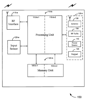
17
CA 02651301 2008-11-04
WO 2007/131052 PCT/US2007/068057
the on/off functionality of one or more of the components of a mobile
communications device
(and also append state information data). Thus, the switch may be configured
to prevent the
operation of the processing unit or memory unit in State 0, while enabling
operation in State
1. Alternatively, the State (0 or 1) could be transmitted with the requested
account
information.
[0066] Next, consider the state diagram 430 of FIG. 4B. In this example, again
assume a
two-state input sensor, the input sensor effectively acting as a switch. When
the switch is off,
at block 435, the input sensor is in a first state, State 0. When the switch
is turned on (e.g.,
via contact, pressure, light, capacitance) at block 440, the input sensor goes
to a second state,
State 1. In this example, when the switch is turned off at block 445 (e.g.,
the contact,
pressure, light, capacitance drops below a set level), the input sensor
returns to the first state,
State 0, after a set period of time (e.g., 5, 10, or 60 seconds). This type of
switch may be used
to control the on/off functionality of one or more of the components of a
mobile
communications device. For example, the switch may be configured to prevent
the operation
of the presentation instrument in State 0, while enabling operation in State
1. Also, the State
(0 or 1) could be transmitted with the requested account information.
[0067] Furthermore, the switch could be a multi-purpose two-state switch. For
example,
assume the applicable components of the mobile communications device are not
functional,
as the switch is off, at block 435. When the switch is turned on (e.g., via
contact, pressure,
light, capacitance) at block 440, the input sensor goes to a second state,
State 1. In this
example, when the switch is turned off at block 445 (e.g., the contact,
pressure, light,
capacitance drops below a set level), the applicable components remain
functional for a
period of time. If the switch is turned on again (e.g., via contact, pressure,
light, capacitance)
during that operational time period, the switch functions to provide state
information for
transmission with the requested account information. Thus, a single two-state
switch may
thereby be configured to 1) provide protection against snooping, and 2)
confirm that the
mobile communications device is possessed by a purchaser.
[0068] Finally, consider the state diagram 460 of FIG. 4C. In this example,
assume a
multi-state input sensor, wherein different combinations of input result in
different states.
For example, there could be various numbered or other configurations of
sensors. Different
combinations of input, received either concurrently or successively, result in
different input
sensor states. Sometimes, a range of inputs will all result in a particular
sensor state. For
18
CA 02651301 2008-11-04
WO 2007/131052 PCT/US2007/068057
purposes of discussion, therefore, the term "range" will be used, but it is
worth noting that a
range may simply comprise a given combination of inputs. Turning to the
exemplary
embodiment illustrated in FIG. 4C, any sensor input in Range A, at block 465,
results in State
A. Similarly, at blocks 470 and 475, each distinct range of inputs, Range B -
Range n, results
in a different State. This type of switch may be used to control the
functionality of applicable
components of the mobile communications device. For example, the input sensor
may be
configured to prevent certain functionality of the processing unit in State A
(e.g., no input),
while enabling operation in all other states. Alternatively, additional
protection may be
provided by rendering the processing unit or certain functions performed
therein available
only if certain passwords, biometric measurements, or other combinations of
inputs (i.e.,
Sensor Ranges) match data stored in the memory unit. Moreover, there could be
different
levels of security (i.e., any input renders processing unit and memory unit
functional, while
only certain ranges of input allow access to a secure region of the memory
unit).
[0069] FIG. 5 illustrates an exemplary system 500 within which various
embodiments of
the invention may operate. The components of such a system may be directly
connected, or
may be connected via a network 515, which may be any combination of the
following: the
Internet, an IP network, an intranet, a wide-area network ("WAN"), a local-
area network
("LAN"), a virtual private network, the Public Switched Telephone Network
("PSTN"), or
any other type of network supporting data communication between devices
described herein,
in different embodiments. A network 515 may include both wired and wireless
connections,
including optical links. Many other examples are possible and apparent to
those skilled in the
art in light of this disclosure. In the discussion herein, a network 515 may
or may not be
noted specifically. If no specific means of connection is noted, it may be
assumed that the
link, communication or other connection between devices may be via a network
515.
[0070] According to various embodiments of the invention, the system 500
includes a host
computer system 520. The host computer system 520 may include, for example,
one or more
server computers, personal computers, workstations, web servers, or other
suitable computing
devices. The host computer system 520 may be fully located within a single
facility or
distributed geographically, in which case a network 515, as described above,
may be used to
integrate different components.
[0071] The host computer system 520 may be in communication with one or more
databases or other data stores, such as PI rules data store 525, financial
institution data stores
19
CA 02651301 2008-11-04
WO 2007/131052
PCT/US2007/068057
530, and financial information data stores 535. According to different
embodiments of the
invention, each data store may include any number of tables and sets of
tables. In addition,
these data stores may be a single database. Application software running on
the host
computer system 520 may query the applicable data stores, and produce
decisions as dictated
by the application software. Each may be incorporated, in whole or in part,
within the host
computer system 520 (e.g., within its storage media), or may be a part of a
separate system
associated with the host computer system 520. Each may be fully located within
a single
facility, or distributed geographically. Each data store may be organized in
any manner
different than described above to provide the functionality called for by the
various
embodiments, as known by those skilled in the art.
[0072] The host computer system 520 is in communication, directly of
indirectly, with the
terminals 505 that communicate directly with the mobile communications devices
540
configured according to various embodiments of the invention. A device 540
may, for
example, be a mobile communications device (100, 150, 175) of FIGs. 1A, 1B, or
1C. A
terminal 505 may be operated by a merchant 510, or may be independent of a
merchant. A
terminal 505 may be a point-of-sale device, a scanner, a smart card reader, or
any other
interface that provides the data connectivity with a device 540. Often, the
terminal 505 also
provides the magnetic field or other source to wirelessly power the applicable
components of
the device 540 to initiate transmission of account information to complete a
transaction.
[0073] By way of example, a terminal 505 requests transaction data (e.g.,
account
information) from a mobile communications device 540 for purposes of
authorizing and
completing a transaction. The device 540 transmits the data related to the
transaction, which
may include any selection from the group consisting of a location, merchant,
time, amount, or
stock keeping unit (SKU) number. Also, the device 540 may include additional
data
regarding the state of the input sensor (whether it be a two-state sensor, or
a sensor that has
additional states). This set of data is received by the host computer system
520.
[0074] The host computer system 520 receives the set of data related to the
transaction, and
accesses the PI rules data stores 525 to determine the handling of the
transaction. The PI
rules data stores 525 includes rules for processing the data received to
identify one or more of
a number of different outputs. Some of the rules relate to the approval or
denial of a
transaction based at least in part on the data representative of the state of
the input sensor.
Other rules may relate to factoring a credit account balance, available
credit, credit history,
CA 02651301 2008-11-04
WO 2007/131052
PCT/US2007/068057
etc. of the holder of the account at issue, or other responsible party.
Therefore, the host
computer system 520 may also query the financial institution data stores 530
(e.g., to get
balance or other account information) and financial information data stores
535 (e.g., to get
credit ratings or history), and may apply this information to the rules as
well. The host
computer system 520 processes the received set of data by applying the set of
data to the
rules.
[0075] The host computer system 520 is then configured to transmit a
responsive output. If
transaction data and the data defining the state of the input sensor are both
received, the host
computer system 520 may authorize or deny the transaction based on the
application of the
rules. The outcome, in some instances, is based at least in part on the data
representative of
the state of the input sensor. If only the transaction data is received (with
no data defining the
state of the input sensor), the rules may include one or more outputs
directing reuse of the
presentation instrument with a valid user input (i.e., with proper state
information).
[0076] FIG. 6 sets forth an exemplary embodiment 600 of the invention,
illustrating a
method of processing a transaction with a mobile communications device. The
method may,
for example, be performed by the mobile communications device (100, 150, 175)
of FIGs.
1A, 1B, or 1C in communication with a host computer system 520 of FIG. 5. At
block 605, a
request for data (e.g., account number data) is transmitted. The requested
data may be
located, for example, on the memory unit of a mobile communications device. At
block 610,
an input sensor (e.g., on the device) will be in one of two state states:
active (i.e., above a
threshold level of contact, pressure, light, capacitance, etc.), or not active
(below a threshold
level of contact, pressure, light, capacitance, etc.). At block 615, if the
input sensor is not
active, there will be no response because the non-active state renders the
applicable
components not functional or not operational. However, if, as at block 620,
the input sensor
is active, the requested data (e.g., account information) is transmitted with
the additional state
information from the input sensor appended, identifying the input sensor as
active. At block
625, the data (i.e. both the requested data and the additional state
information) is received and
applied to rules in a PI rules database (e.g., by the host computer system).
At block 630, an
authorization is output (e.g., by based at least in part on information from
the input sensor).
[0077] FIG. 7 sets forth another exemplary embodiment 700 of the invention,
illustrating
an alternative method of processing a transaction with a device. The method
may, for
example, be performed by the mobile communications device (100, 150, 175) of
FIGs. 1A,
21
CA 02651301 2008-11-04
WO 2007/131052
PCT/US2007/068057
1B, or 1C in communication with a host computer system 520 of FIG. 5. At block
705, a
request for data (e.g., account number data) is transmitted (e.g., by a point
of sale device).
The data may be located on the memory unit of the mobile communications
device. At block
710, an input sensor will be in one of two states, which will be referred to
in this example as
"on" or "off." At block 715, if the input sensor is in the off state, there
will be no response
because the non-active state renders applicable components of the mobile
communications
device not functional or operational. However, as illustrated at block 720,
the input sensor
may alternatively be in the "on" state, and if so will remain there for a
specified period of
time (e.g., because when the input sensor crosses above or below a threshold
level of contact,
pressure, light, or capacitance, the sensor remains in the "on" state for at
least a period of
time). If "on," the mobile communications device at block 725 transmits the
requested data
(e.g., account information, location, amount, merchant, etc.), but does not
transmit additional
state information from the input sensor.
[0078] At block 730, the received data is applied to rules in PI rules
database (e.g., by a
host computer system). At block 735, a directive is output to resubmit the
presentation
instrument with proper information from the input sensor, as called for by the
rules. At block
740, the device (perhaps via a point of sale terminal) receives the directive
within its
operational time period (i.e., before it has returned to the off state). At
block 745, the device
transmits the requested data with the state information from the input sensor.
At block 750,
received data (including the input from the input sensor) is applied (e.g., by
the host computer
system) to rules in PI rules database. At block 755, an authorization is
output based at least
in part on the input sensor information. This flow chart provides an example
of the possible
interrelation between the mobile communications device functionality
(illustrated by the
dashed line identified by reference numeral 760) and the host computer system
functionality
(illustrated by the dashed line identified by reference numeral 765).
[0079] A device structure 800 that may be used for a host computer, server,
point-of-sale
device, terminal, reader, mobile communications device or other computing
device described
herein is illustrated with the schematic diagram of FIG. 8. This drawing
broadly illustrates
how individual system elements of each of the aforementioned devices may be
implemented,
whether in a separated or more integrated manner. The exemplary structure is
shown
comprised of hardware elements that are electrically coupled via bus 805,
including
processor(s) 810 (which may further comprise a DSP or special-purpose
processor), storage
device(s) 815, input device(s) 820, and output device(s) 825. The storage
device(s) 815 may
22
CA 02651301 2008-11-04
WO 2007/131052
PCT/US2007/068057
comprise a computer-readable storage media reader connected to any computer-
readable
storage medium, the combination comprehensively representing remote, local,
fixed, or
removable storage devices or storage media for temporarily or more permanently
containing
computer-readable information. The communications/power interface(s) 845 may
comprise a
wired, wireless, or other type of interfacing connection and/or antenna that
permits data
and/or power to be exchanged with other devices. The communications/power
interface 845
may permit data to be exchanged with a network (including, without limitation,
the Network
515).
[0080] The structure 800 may also include additional software elements, shown
as being
currently located within working memory 830, including an operating system 835
and other
code 840, such as programs or applications designed to implement methods of
the invention.
The structure may include a GPS or other Location Receiver 850, to receive and
provide
location based data. It will be apparent to those skilled in the art that
substantial variations
may be used in accordance with specific requirements. For example, customized
hardware
might also be used, or particular elements might be implemented in hardware,
software
(including portable software, such as applets), or both.
[0081] It should be noted that the methods, systems and devices discussed
above are
intended merely to be exemplary in nature. It must be stressed that various
embodiments
may omit, substitute, or add various procedures or components as appropriate.
For instance,
it should be appreciated that in alternative embodiments, the methods may be
performed in an
order different than that described, and that various steps may be added,
omitted or
combined. Also, features described with respect to certain embodiments may be
combined in
various other embodiments. Different aspects and elements of the embodiments
may be
combined in a similar manner. Also, it should be emphasized that technology
evolves and,
thus, many of the elements are exemplary in nature and should not be
interpreted to limit the
scope of the invention.
[0082] Specific details are given in the description to provide a thorough
understanding of
the embodiments. However, it will be understood by one of ordinary skill in
the art that the
embodiments may be practiced without these specific details. For example, well-
known
circuits, processes, algorithms, structures, and techniques have been shown
without
unnecessary detail in order to avoid obscuring the embodiments.
23
CA 02651301 2013-07-31
[0083] Also, it is noted that the embodiments may be described as a process
which is
depicted as a flowchart, a data flow diagram, or a block diagram. Although
these diagrams
may describe the operations as a sequential process, many of the operations
can be performed
in parallel or concurrently. In addition, the order of the operations may be
re-arranged. A
process is terminated when its operations are completed, but could have
additional steps not
included in the figure.
[0084] Moreover, as disclosed herein, the terms "memory unit" and "means for
storing
data" may represent one or more devices for storing data, including read only
memory
(ROM), random access memory (RAM), magnetic RAM, core memory, magnetic disk
storage mediums, optical storage mediums, flash memory devices or other
machine readable
mediums for storing information. The term "computer-readable medium" includes,
but is not
limited to, portable or fixed storage devices, optical storage devices,
wireless channels, a sim
card, other smart cards, and various other mediums capable of storing,
containing or carrying
instructions or data.
[0085] Furthermore, embodiments may be implemented by hardware, software,
firmware,
middleware, microcode, hardware description languages, or any combination
thereof. When
implemented in software, firmware, middleware or microcode, the program code
or code
segments to perform the necessary tasks may be stored in a computer readable
medium, such
as a memory unit. Processors may perform the necessary tasks.
[0086] Having described several embodiments, it will be recognized by those of
skill in the
art that various modifications, alternative constructions, and equivalents may
be used without
departing from the scope of the invention. For example, the above elements may
merely be a
component of a larger system, wherein other rules may take precedence over or
otherwise
modify the application of the invention. Also, a number of steps may be
required before the
above elements are considered. Accordingly, the above description should not
be taken as
limiting the scope of the invention, which is defined in the following claims.
24