Note: Descriptions are shown in the official language in which they were submitted.
CA 02651434 2008-11-06
WO 2007/134444 PCT/CA2007/000891
APPARATUS AND METHOD FOR ESTABLISHING DEVICE IDENTIFIERS
FOR SERIALLY INTERCONNECTED DEVICES
FIELD OF THE INVENTION
The present invention relates generally to semiconductor device systems. More
particularly, the present invention relates to apparatus and method for
establishing device
identifiers synchronously with a clock signal for a serial interconnection
configuration of
devices.
BACKGROUND OF THE INVENTION
Today computer-based systems can be found most everywhere and have made
inroads into many devices that are used everyday, such as cell phones,
handheld
computers, automobiles, medical devices, personal computers and the like. In
general,
society has placed much reliance on computer-based systems to handle everyday
tasks,
such as simple tasks like balancing checkbooks to relatively complex tasks
such as
predicting the weather. As technology improves, more and more tasks are
migrated to
computer-based systems. This, in turn, causes society to become more and more
reliant on
these systems.
A typical computer-based system comprises a system board and optionally one or
more peripheral devices, such as display units and disk units. The system
board often
contains one or more processors, a memory subsystem and other circuitry, such
as serial
device interfaces, network device controllers and hard disk controllers.
The type of processors employed on a particular system board usually depends
on
the type of tasks performed by the system. For example, a system that performs
a limited
set of tasks, such as monitoring emissions generated by an automobile engine
and
adjusting an air/fuel mixture to ensure the engine is burning fuel completely,
may employ
a simple specialized processor that is tailored to performing these tasks. On
the other
hand, a system that performs many different tasks, such as managing many users
and
running many different applications, may employ one or more complex processors
that are
general purpose in nature, configured to perform high-speed calculations and
manipulate
data to minimize the response time to servicing the users' requests.
CA 02651434 2008-11-06
WO 2007/134444 PCT/CA2007/000891
The memory subsystem is storage that holds information (e.g., instructions,
data
values) used by the processors. The memory subsystem typically comprises
controller
circuitry and one or more memory devices. The controller circuitry is usually
configured
to interface the memory devices with the processors and enable the processors
to store and
retrieve information to and from the memory devices. The memory devices hold
the
actual information.
Like the processors, the type of devices employed in a memory subsystem is
often
driven by the type of tasks performed by the computer system. For example, a
computer
system may have the task of having to boot without the assistance of a disk
drive and
execute a set of software routines that do not change often. Here, the memory
subsystem
may employ non-volatile devices, such as flash memory devices, to store the
software
routines. Other computer systems may execute very complex tasks that require a
large
high-speed data store to hold large portions of information. Here, the memory
subsystem
may employ high-speed high-density Dynamic Random Access Memory (DRAM) devices
to store the information.
Demand for flash memory devices has continued to grow significantly because
these devices are well suited in various embedded applications that require
non-volatile
storage. For example, flash is widely used in various consumer devices, such
as digital
cameras, cell phones, USB flash drives and portable music players, to store
data used by
these devices. Market demand for flash memory has led to tremendous
improvements in
flash memory technology over the past several years both in terms of speed and
density.
These improvements have led to the prediction that flash memory-based devices
may one
day replace hard disk drives in applications that continue to use disk drives
for mass
storage.
Some flash devices employ serial interfaces such as, for example, multiple
flash
devices, which are used to perform operations, such as read, write and erase
operations, on
memory contained in the devices. These operations are typically selected on a
device
using command strings that are serially fed to the devices. The command
strings typically
contain a command that represents the operation to be selected, as well as
other
parameters. For example, a write operation may be selected by serially feeding
an
-2-
CA 02651434 2008-11-06
WO 2007/134444 PCT/CA2007/000891
information string to the device that contains a write command, the data to be
written and
an address in the memory where the data is to be written.
The command string may be fed to all of the devices even though the command
may only be performed on one of the devices. To select the device on which the
command is to be performed, the command string may contain a device identifier
(ID) that
identifies the flash device to which the command is directed. Each device
receiving the
command string compares the device ID contained in the command string to an ID
associated with the device. If the two match, the device assumes that the
command is
directed to the device and performs the command.
A problem with the above-described arrangement involves establishing a device
ID
for each device. One technique that may be used to establish a device ID for a
device is to
hardwire an internal unique device ID into the device. A drawback with this
approach,
however, is that if large volumes of devices are produced, the size of the
device ID may
have to be quite large in order to ensure that each device contains a unique
device ID.
Managing a large-sized device ID may add significant complexity to the device,
which in
turn may increase the cost of producing the device. In addition, reclaiming
device IDs that
are associated with devices that are no longer in use may further add to the
complexity of
this scheme.
Another approach to assigning device IDs to devices involves externally
hardwiring a device ID for each device. Here, the device ID may be specified
by wiring
various pins on the device to certain states to establish a device ID for the
device. The
device reads the wired state of the pins and establishes its ID from the read
state. One
drawback with this approach, however, is that external wiring is needed to
assign the
device ID for each device. This may add to the complexity of, e.g., printed
circuit boards
(PCBs) that hold the memory devices. Another drawback with this approach is
that it may
require pins to be dedicated for the assignment of the device ID. This may
consume
precious resources that may be otherwise better used. In addition, dedicating
pins for the
assignment of the device ID may require a greater footprint for the device
than if pins
were not used to assign the device ID.
One of the solutions proposed to address the aforementioned limitations of
prior art
techniques is to automatically establish a device identifier (ID) for a
device, for example,
-3-
CA 02651434 2008-11-06
WO 2007/134444 PCT/CA2007/000891
in a serial interconnection configuration, in a manner that does not require
special internal
or external hardwiring of the device ID. Such a technique is taught in related
U.S. Patent
Application No. 11/521,734 filed September 15, 2006, the teachings of which
are
incorporated herein by reference in their entirety. Briefly, the technique
enables the role
of Input Port Enable (IPE) signal to change based on the device configuration
of single
chip, multi-drop, or serial interconnection. The serial input (SI) and serial
output (SO)
functions can send and receive all data types without timing restriction
during relevant
operations. There is also no need for additional pin or pin function change
from the main
pin definition. This ID generation and assignment technique depends on the
number of
available pins, which are determined by the number of link ports. Therefore,
for example,
in multi-independent serial link (MISL), for single port, the maximum number
of devices
supported is eight devices. In the case of dual ports, the maximum number of
devices is
64 (i.e., three pins for one port).
SUMMARY OF THE INVENTION
An apparatus and method for establishing device identifiers for a serial
interconnection configuration of devices is disclosed. The devices may be, for
example,
memory devices, such as dynamic random access memories (DRAMs), static random
access memories (SRAMs) and flash memories. Such serial interconnection may be
implemented in a multi-independent serial link (MISL).
Aspects of the technique enable identifiers to be assigned to devices without
requiring additional hard pins on the device for this purpose. Using
functional and timing
definitions, an identifier of each device is automatically produced by a
device that contains
related combination logic, such as an adder.
In a first aspect, the present invention provides an apparatus for
establishing a
device identifier (ID) for a device configured in a serial interconnection
configuration
having a plurality of devices. The apparatus comprises an ID producer for
producing a
device ID in response to an input signal received at a serial input of the
device, and
outputting an output signal associated with a produced device ID through a
serial output of
the device synchronously with clock.
-4-
CA 02651434 2008-11-06
WO 2007/134444 PCT/CA2007/000891
In one example, the input signal received at the device includes a value
associated
with the device ID of the device and the produced device ID associated with
the output
signal includes a value associated with the device ID of another device in the
serial
interconnection configuration.
In another example, the input signal received at the device includes a value
associated with the device ID of a previous device in the serial
interconnection
configuration and the produced device ID associated with the output signal
includes a
value associated with the device ID of the device of the serial
interconnection
configuration.
In a further embodiment, the ID producer comprises: an ID calculator for
making
an N-bit ID and producing a calculated value based on the N-bit ID and a
predetermined
number, N being an integer that is one or greater than one; and an ID provider
for
providing the device ID in accordance with the calculated value.
For example, the ID calculator performs a calculation of adding 1 to the N-bit
ID
and the addition result is provided as the N-bit ID. Alternatively, the
calculation may be
performed by subtracting 1 from the N-bit ID and the subtraction result is
provided as the
N-bit ID.
The technique also provides an apparatus for generating a device identifier
(ID) for
a device coupled to one of a plurality of devices in a serial interconnection
configuration.
The device can have at least one cell for storing data, a serial input
connection for
receiving serial input data and a serial output connection for providing
serial output data.
The apparatus includes an input registering circuit for registering serial N-
bit ID data
contained in the serial input data and for providing the registered N-bit ID
data as parallel
N-bit ID data, N being an integer that is one or greater than one; a
calculating circuit for
performing a calculation based on the parallel N-bit ID data and given number
data to
provide N-bit calculation data; and a parallel-serial circuit for registering
the N-bit
calculation data as parallel N-bit calculated data and for providing the
registered parallel
N-bit calculated data in as serial N-bit data, the serial N-bit data being
forwarded to an
input registering circuit included in another generating apparatus coupled to
another
device.
-5-
CA 02651434 2008-11-06
WO 2007/134444 PCT/CA2007/000891
For example, the device can be a memory device that includes a calculating
circuit
having a circuit for adding the given number data to the parallel N-bit ID
data or
subtracting the given number data from the parallel N-bit ID data to generate
a new ID.
For example, the adding circuit or subtracting circuit can include an N-bit
adder or
subtractor, which performs parallel addition or subtraction. The parallel
added or
subtracted data is fed to an N-bit parallel-to-serial register, which in turn
provides serial ID
data that is transferred to another memory device.
The apparatus can include a selector that selects the serial N-bit data to be
forwarded to another generating apparatus coupled to another memory device, in
response
to an ID generation enabling signal. The ID generation enabling signal may be
generated
in accordance with commands included in the serial input data. The selector
may select
data derived from the cell for storing data in the memory device and
forwarding the data to
the other memory device, in accordance with the status of the ID generation
enabling
signal.
In a further aspect, the present invention provides a device configured in a
serial
interconnection configuration of a plurality of devices, the device comprising
a device
identifier (ID) establisher for establishing a device ID for the device. The
device ID
establisher includes an ID generator for: generating a device ID in response
to an input
signal received at a serial input of the device; and outputting an output
signal associated
with a generated device ID through a serial output of the device synchronously
with clock.
In another aspect, the present invention provides a serial interconnection
configuration of a plurality of devices. Each of the devices comprises: a
serial input and
serial output for, respectively, receiving an input signal and transferring an
output signal; a
clock input for receiving a clock signal; and a device identifier (ID)
establisher for
establishing a device ID for the device, the device ID establisher having an
ID generator
for generating a device ID in response to the input signal received at the
serial input of the
device, the output signal being associated with a generated device ID through
the serial
output of the device synchronously with clock.
In yet another aspect, the present invention provides a method for
establishing a
device identifier (ID) for a device configured in a serial interconnection
configuration
having a plurality of devices. The method comprises: generating a device ID in
response
-6-
CA 02651434 2008-11-06
WO 2007/134444 PCT/CA2007/000891
to a serial input signal; and outputting a signal associated with the device
ID through a
serial output of the device. The generating and transferring are synchronous
with clock.
Other aspects and features of the present invention will become apparent to
those
ordinarily skilled in the art upon review of the following description of
specific
embodiments of the invention in conjunction with the accompanying figures.
BRIEF DESCRIPTION OF THE DRAWINGS
Embodiments of the present invention will now be described, by way of example
only, with reference to the attached Figures, wherein:
Fig. 1A is a block diagram of a device configuration comprising a plurality
of single port devices configured in a serial interconnection configuration,
in which
embodiments of the present invention may be implemented;
Fig. 1B is a block diagram illustrating one of the devices shown in Fig. 1A;
Fig. 2A is a block diagram illustrating communications between devices
configured in a serial interconnection configuration;
Fig. 2B is a timing diagram illustrating communication between devices
configured in the serial interconnection configuration as shown in Fig. 2A;
Figs. 3A and 3B are, respectively, a block diagram of devices employing an
example of ID generation logic for single link and a timing diagram of signals
for
the memory devices;
Figs. 4A and 4B, are, respectively, a block diagram of devices employing
an example of ID generation logic for dual link and a timing diagram of
signals for
the devices;
Fig. 5A is a high-level block diagram of logic that can be used to generate
an ID for a device according to an embodiment of the present invention;
Fig. 5B is a detailed block diagram of the logic shown in Fig. 5A;
Fig. 5C is a block diagram of an ID generator shown in Figs. 5A and 5B;
Fig. 6 is an illustration of a timing diagram of clock generation for a device
number (DN) register and a command register;
Fig. 7 is an illustration of a timing diagram of an ID generation;
-7-
CA 02651434 2008-11-06
WO 2007/134444 PCT/CA2007/000891
Fig. 8 is an illustration of a timing diagram of latency in the normal
operation mode;
Fig. 9A is an illustration of a timing diagram of ID generation controlled by
an output port enable signal;
Fig. 9B is an illustration of an ID bit length control by the output port
enable signal;
Fig. 10 is an illustration of a timing diagram of an ID output enable signal,
a shift clock signal and other signals;
Fig. 11 is an illustration of a timing diagram of an ID generation and related
signals;
Fig. 12A is a block diagram illustrating an ID temporary register
configuration;
Fig. 12B is an illustration of a timing diagram of signals for an ID
temporary register;
Fig. 13A is a high-level block diagram of logic that can be used to generate
an ID for a device according to a second embodiment of the present invention;
Fig. 13B is a detailed block diagram of the logic shown in Fig. 13A;
Fig. 13C is a block diagram of an ID generator shown in Figs. 13A and
13B;
Fig. 14 is an illustration of an ID bit length control by an output port
enable
signal for the embodiment shown in Fig 13A;
Fig. 15A is a high-level block diagram of logic that can be used to generate
an ID for a device according to a third embodiment of the present invention;
Fig. 15B is a detailed block diagram of the logic shown in Fig. 15A;
Fig. 15C is a block diagram of an ID generator shown in Figs. 15A and
15B;
Fig. 16 is an illustration of a timing diagram of signals for the ID
generation logic illustrated in Fig. 15A; and
Fig. 17 is an illustration of an ID bit length control by an output port
enable
signal for the embodiment shown in Fig. 15A.
-8-
CA 02651434 2008-11-06
WO 2007/134444 PCT/CA2007/000891
DETAILED DESCRIPTION
Generally, the present invention provides a system including a number of
devices
in a serial interconnection configuration. An apparatus and a method for
establishing
device identifiers for a serial interconnection configuration of devices are
disclosed. Such
serial interconnection may be implemented in a multi-independent serial link
(MISL).
The method and apparatus in accordance with the techniques described herein
may
be applicable to a memory system having a plurality of devices in a serial
interconnection.
The devices may be, for example, memory devices, such as dynamic random access
memories (DRAMs), static random access memories (SRAMs) and flash memories.
In conventional memory devices, ID assignment is typically performed using
additional pins to make a logic combination, such as (0000), (0001), ....,
(1111).
Assigning IDs in this manner typically means that pin assignment should be
mandatory to
cover the connection.
Serializing commands and data applied to a memory device enables fewer pins to
be employed to perform various functions associated with the device. ID
assignment to a
particular memory device may be performed using serial input enable and output
enable
signal ports associated with the device. Here, a number associated with the
device's ID
may be transferred and incremented by one into each device serially. No
complicated
timing need be generated. Entry timing and exit timing may be used for the ID
write
operation of device.
Generally, aspects of the present invention provide a method and a device
controller for establishing a device identifier (ID) for a device configured
in a serial
interconnection configuration having a plurality of devices, the device
controller
comprising: an ID generator for generating a device ID associated with a first
device in
response to an input signal received at a serial input of the first device,
and transferring an
output signal associated with the device ID to a second device in the serial
interconnection
configuration through a serial output of the first device synchronously with a
clock signal.,
as described in detail below.
With reference to the figures, embodiments of the present invention will be
described. In the following description, the same reference signs will be used
for signals
-9-
CA 02651434 2008-11-06
WO 2007/134444 PCT/CA2007/000891
and input and output connections. For example, reference sign CLK represents a
clock
signal and a clock input connection; IPE represents an input port enable
signal and an
input port enable input connection of a device; OPE represents an output
enable signal and
an output port enable connection of a device; CS# represents a chip select
signal and a
chip select input connection; IPEQ represents an input port enable output
connection of a
device and an input port enable output signal; and OPEQ represents an output
port enable
output connection of a device and an output enable output signal.
Fig. 1A shows an exemplary device configuration including a plurality of
single
port devices configured in a serial interconnection configuration having
inputs and outputs
for various signals. In this particular example, the device configuration
includes four
devices 0, 1, 2, and 3(110-1, 110-2, 110-3, and 110-4). Each of the
interconnected devices
110-1 - 110-4 has the same structure. A memory controller (not shown) provides
a group
of signals containing chip select CS#, serial input (SI), input port enable
(IPE), output port
enable (OPE)_, clock CLK, and other control and data information (not shown)
that are
provided to the devices. A memory system may include such a serial
interconnection
configuration of devices and a memory controller for controlling operations of
the serially
interconnected devices.
Fig. 1B shows one device 110-i representing any one of the devices 110-1 - 110-
4
shown in Figure 1A. The device 110-i includes a device controller 130 and a
memory 120
including such as, for example, random access memory or Flash memory. For
example,
the random access memories can be dynamic random access memory (DRAM), static
random access memory (SRAM), magnetoresistive random access memory (MRAM) and
the Flash memories can be NAND-type, NOR-type, AND-type, and other types of
Flash
memories. The device controller 130 has a device identifier (ID) generator
140. The
device 110-i has a serial input port (SIP) connection, a serial output port
(SOP)
connection, a chip select input (CS#), and a clock input (CLK). The SIP is
used to transfer
information (e.g., command, address and data information) into the device 110-
i. The SOP
is used to transfer information from the device 110-i. The CLK input receives
a clock
signal. The CS# input receives a chip select signal CS#, which enables
operations at all
devices simultaneously. The device controller 130 performs various control and
process
functions with access to the memory 120 in response to the input signals
(e.g., SI, IPE,
OPE, CLK), and provides serial output data to the next device 110-(i+1).
-10-
CA 02651434 2008-11-06
WO 2007/134444 PCT/CA2007/000891
Referring to Figs. lA and 1B, the SIP and the SOP are connected between
devices
in the serial interconnection configuration such that the SOP of previous
device 110-(i-1)
in the serial interconnection is coupled to the SIP of the device 110-i in the
serial
interconnection. For example, the SOP of device 1, 110-1, is coupled to the
SIP of device
2, 110-2. The CLK input of each of four devices 110-1 - 110-4 is fed with the
clock signal
CLK from the memory controller (not shown). The clock signal CLK is
distributed to all
devices via a common link. As will be described further below, the clock
signal CLK is
used to, inter alia, latch information input to the device 110-i at various
registers contained
therein. The CS# input is a conventional chip select input for selecting the
device. The
CS# input is coupled to a common link, which enables the chip select signal
CS# to be
asserted to all of the devices 110-1 - 110-4 concurrently and consequently
selects all of
the devices.
In addition, the device 110-i has an input port enable (IPE) input, an output
port
enable (OPE) input, an input port enable output (IPEQ) and an output port
enable output
(OPEQ). The IPE is used to input the input port enable signal IPEi to the
device 110-i. The
signal IPEi is used by the device to enable the SIP such that when the IPE is
asserted,
information is serially input to the device 110-i via the SIP. Likewise, the
OPE is used to
input the output port enable signal OPEi to the device 110-i. The OPEi signal
is used by
the device to enable the SOP such that when the OPE is asserted, information
is serially
output from the device 110-i via the SOP. The IPEQ and the OPEQ are outputs
that output
the IPEQi and OPEQi signals, respectively, from the device 110-i. The CS# and
the CLK
inputs are coupled to separate links which distribute the chip select signal
CS# and the
clock signal CLK, respectively, to four devices 110-1 - 110-4, as described
above.
The SIP and the SOP are coupled from previous device 110-(i-1) to next device
11 0-(i+ 1) in the serial interconnection configuration, as described above.
Moreover, the
IPEQ and the OPEQ outputs of the previous device 110-(i-1) are coupled to the
IPE and
the OPE inputs, respectively, of the present device 110-i in the serial
interconnection
configuration. This arrangement allows the IPE and OPE signals to be
transferred from
one device to the next (e.g., device 0, 110-1, to device 1, 110-2) in the
serial
interconnection configuration.
-11-
CA 02651434 2008-11-06
WO 2007/134444 PCT/CA2007/000891
Information transmitted to the devices 110-1 - 110-4 can be latched at
different
times of the clock signal CLK fed to the CLK input. For example, in a single
data rate
(SDR) implementation, information input to the device 110-i at the SIP can be
latched at
either the rising or falling edge of the clock signal CLK. Alternatively, in a
double data
rate (DDR) implementation, both the rising and falling edges of the clock
signal CLK can
be used to latch information input at the SIP.
The configuration of the devices 110-1 - 110-4 in Fig. 1A includes both a
serial
interconnection (e.g., input SI and output SO) and conventional multi-drop
connections
(e.g., CLK and CS#). Thus, the configuration may be referred to as a hybrid of
serial
interconnection and multi-drop configurations, where the advantages of each
may be
realized.
The ID generator 140 generates an ID to establish a device ID for the device
in the
serial interconnection configuration.
Figs. 2A and 2B illustrate three devices 210-1 - 210-3 configured in a serial
interconnection with an accompanying timing diagram showing signals
transferred
between the devices. A chip select signal CS# (not shown) is first asserted to
select the
devices. Information is transmitted to the first device 210-1 in the serial
interconnection by
asserting IPE and clocking data into the device 210-1 on successive rising
edges of the
clock signal CLK. An input port enable signal IPE is propagated through the
first device
210-1 to the second device 210-2 in less than a cycle, as shown by signal
IPE_0. The
propagation enables information to be clocked from the SOP of the first device
210-1 to
the SIP input of the second device 210-2 at one cycle after the information
was clocked
into the first device 210-1. This process is repeated for successive devices
in the serial
interconnection. For example, information is inputted to the third device 210-
3 in the serial
interconnection at the third rising edge of the clock signal CLK from the
latch point of the
data at the first device 210-1. Control signals IPE_0, IPE_1, IPE_2 are
synchronized with
the rising edge of the signal CLK in order to ensure a proper setup time for
these signals at
the next device in the serial interconnection configuration.
Figs. 3A and 4A illustrate exemplary operations to generate device identifiers
(IDs) for memory devices in a serial interconnection configuration for single
and dual
links, respectively. Fig. 3A depicts devices 310-1 -, 310-m and 310-n
connected in a
-12-
CA 02651434 2008-11-06
WO 2007/134444 PCT/CA2007/000891
single link arrangement and Fig. 3B depicts signal timings for the devices
shown in Fig.
3A. Similarly, Fig. 4A depicts devices 410-1 -, 410-m and 410-n connected in a
dual link
arrangement and Fig. 4B depicts signal timings for the devices shown in Fig.
4A. Here, n
is an integer greater than one and m is (n-1). In the particular examples
shown in Figs. 3A
and 4A, each of the devices includes a device controller having an ID
generator that is
similar to that of Fig. 1B.
This exemplary operation generates device IDs using two inputs of a serial
interconnection, the SIP and SOP inputs, and can be adapted for use with other
ports in a
serial interconnection, where a first input receives a serial input and a
second port receives
a control signal. The ID generation techniques are not limited to MISL
application and can
be applicable to any serial connection configurations (e.g., daisy cascading
connection)
with a plurality of existing input pins, if the serial connection (e.g., a
daisy chain) system
has a clock.
In this embodiment, the IPE has a function to catch a serial input stream
based on
the 1 byte unit so that the OPE is chosen to latch a serial ID input stream
after the chip
select signal CS# is low again. By `write ID entry' command, the OPE catches
an input
stream which consists of the same cycles as a total number of ID bits. The ID
bits are
established by the size of an internal ID register. For example, if the
devices have a 12 bit-
ID register, the OPE will hold the `high' state during 12 cycles. A 12-bit
device ID allows
for a maximum of 4,096 addresses in the serial interconnection. Thus, the
present
embodiment may accommodate a large number of devices in a serial
interconnection
configuration, the number not being limited by the number of pins at each
device. Further,
each device does not require the added complexity of an internal hardwired
device ID.
In Figs. 3B and 4B, an ID generation mode setting period referenced at "IDGMS"
is a time interval equivalent to pre-defined clock cycles corresponding to the
ID bit length
+ eight cycles (command bit length) + an assumed number of serially
interconnected
devices.
For a signal transfer between the OPE input and the OPEQ output or opl and
op2,
a non-overlap time section of more than two cycles should occur to avoid an
operation
contention caused by an ID increment and data transferring to an adjacent next
device.
After the OPE is asserted at each device 310-1 - 310-n, latched ID input data
is stored in
-13-
CA 02651434 2008-11-06
WO 2007/134444 PCT/CA2007/000891
an ID register (e.g. referenced at "516" in Fig. 5A) of the device and
increment operation
with this input is performed before asserting the OPEQ output. A function of
the OPE
signal is to determine the number of ID bits from 1 bit to the maximum number
of defined
bits of the ID register into each memory device. In cases where the number of
ID bits and
the number of defined bits of the ID register are equal ("fixed ID bit"), the
order of the ID
bits is irrelevant. However, in all other cases, the signal corresponding to
device ID
should be transferred to the next device in order, beginning with the least
significant bit
(LSB) and ending with the most significant bit (MSB), reasons for which will
be described
later.
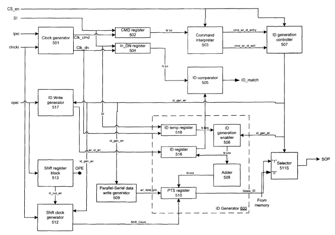
Figs. 5A and 5B illustrate exemplary logic associated with ID generation of
device
controller 500 internal to a device 110-i configured in a serial
interconnection. A clock
generator 501 receives a clock signal fed to the CLK input of the device and
provides
internal clock signals including "Clk_cmd" and "Clk dn." The command clock
`clk_cmd'
is asserted a number of times equal to the bit length of command serial bits.
As shown in
Fig. 6, for example, if the memory system has a command of 1 byte unit, the
clk cmd
needs 8 clock cycles to latch the serial command bits and then hold latched
data until the
next command received. The device number (DN) clock `clk_dn' clocks the ID
input,
which is stored in input DN register 504 and ID temporary register 518. The
sequence of
receiving and storing the signals received at the SIP input corresponds to a
predefined
sequence. For example, the devices may be configured to first receive a signal
corresponding to a device ID, followed by receiving command bits. As a result
of this
order, a number of cycles of clk dn are generated and then clk cmd is issued
by the clock
generator 501.
In order to decode the command bits, serial input command streams are shifted
into
command register 502 in response to the command clock `clk_cmd,' and command
register 502 in turn sends the registered M-bit command data in parallel to
command
interpreter 503. The command interpreter 503 is a command decoder and delivers
internal
command signals that initiate additional controls. Two such command signals
(cmd wr id entry, cmd_wr id exit) are depicted, and function to start and stop
the ID
generation mode.
-14-
CA 02651434 2008-11-06
WO 2007/134444 PCT/CA2007/000891
Prior to the ID write generator issuing the command `write ID entry,' the
memory
controller (not shown) sends a reset signal to reset inputs of the devices of
the serial
interconnection configuration. The reset inputs are commonly connected. All
devices in
the serial interconnection configuration are reset by the reset signal. Upon
resetting, all
devices are enabled to accept the `write ID entry' command by default, and all
devices
have a default ID of `zero.' As a result, all devices in the serial
interconnection can be
selected at the same time, and the command `write ID entry' instructs all
devices by
having a command `ID number' of `zero.'
The input DN register 504 stores input ID data from the previous device.
During
normal operation (rather than ID generation mode), the input DN register 504
temporarily
stores the content of input ID streams from the SIP to be compared with a
device ID
number in the N-bit ID register 516 (e.g., a 10-bit register). During device
ID generation,
the input DN register 504 does not receive serial input data. Instead, the ID
temporary
register 518 catches the serial data and sends it to an ID producer or
establiser,
exemplified as ID generation enable block 506. The bit number N is an integer
that equals
the number of bits in the ID number, and can equal any number suitable to
identify all
devices in the serial interconnection.
The ID comparator 505 functions during normal device operation to identify
data
and command signals addressed to the device. The comparator 505 compares the
ID
number of each incoming data at input DN register 504 to the device ID stored
in the N-
Bit ID register 516, and provides an `ID_match' signal. If the ID numbers are
identical or
match, the ID_match signal will equal `1.' Otherwise, it will equal V. As a
result, each
device in the serial interconnection determines whether signals are addressed
to it by
matching incoming ID number to the device ID stored at each device.
Fig. 5C shows an ID generator 600 of the device controller 500 of Figs. 5A and
5B. In response to an 'id_gen_en' (ID generation enable) signal from an ID
generation
controller 507, the ID generation enable block 506 transfers the N-bit inputs
of the ID
temporary register 518 to the calculator, exemplified as N-bit adder 508
(e.g., a 10-bit
adder), and the N-bit ID register 516. Exemplary signal timing for ID
generation enable
signal is illustrated in Fig. 7. This simultaneous transfer prevents an
unnecessary signal
transition of the N-bit adder 508 and the N-bit ID register 516. The device ID
is stored in
-15-
CA 02651434 2008-11-06
WO 2007/134444 PCT/CA2007/000891
the ID register 516 according to the sequence and word length of the device
ID. For
example, if the N-bit ID register 516 is 10-bits in length and the OPE signal
has a 5-cycle
high state, then the N-bit ID register 516 stores the 5-bit device ID and a
signal
corresponding to the 5-bit device ID is transferred to the next device. The
remaining bits
of the ID register 516 are ignored and thus remain at a value of `0' or `don't
care'.
During the ID generation process, in the above-described example, the N-bit
serial
input is first stored in the ID temporary register 518 prior to being
transferred to the N-bit
adder 508 and the N-bit ID register 516. The simultaneous transfer from the
temporary
register overcomes limitations of serial to parallel (STP) registers. For
example, consider a
case where the number of ID bits (say, 5 bits) is less than the number of bits
of the ID
register and adder (say, 10 bits). During the ID generation and assignment
process, the five
bits (bit 0 (LSB) to bit 4(MSB)) are loaded to the first five bits of a STP
register and are
then provided in parallel to a 10-bit adder. As will be readily apparent to a
person skilled
in the art, the LSB will be located on bit 4 of the register, which does not
correspond to the
LSB of the adder. Even if the order of the bits were reversed from MSB (bit 0)
to LSB (bit
4), the location of MSB in the STP register will not correspond to the MSB
location of the
10-bit adder. Therefore, no matter which bit is assigned as a first bit,
conventional STP
registers will result in generating erroneous device IDs. This limitation of
STP registers is
overcome by ensuring that the bits corresponding to the device ID are
transferred to the
next device in order, beginning with the LSB and ending with the MSB, and
storing them
in the order received in the ID temporary register (LSB to bit 0 of ID
temporary register
518), as will be discussed later in detail with reference to Figs. 12A and
12B.
The ID generation controller 507 receives the input signals CS# (CS_en),
cmd wr id_entry, and cmd wr id exit, and transmits the `id gen_en' signal,
which
begins the ID generation mode. The `id gen_en' signal is asserted, for
example, when the
signal CS# is toggled from low to high and low again (see Fig. 7), while the
signal
cmd wr id entry is asserted simultaneously. It is noted that `id_gen_en' can
be asserted
with any other transition of the signal CS# as will be apparent to persons
skilled in the art.
Fig. 8 shows latency in the normal operation. Basically, MISL has a one-cycle
latency between two adjacent devices. However, `write ID entry' command makes
a
-16-
CA 02651434 2008-11-06
WO 2007/134444 PCT/CA2007/000891
change of the path from 1 cycle latency to `ID bits (ID register bit size) + 2
cycles', as
shown in Fig. 9A described below.
Figs. 9A and 9B illustrate logic and signal timing of an ID generation control
by
the output port enable (OPE) signal. Under this operation, the ID bit length
can be
determined by the length of the OPE signal high, and can be adapted to a
serial
interconnection configuration including different numbers of devices. The
function of the
OPE signal is described below with reference to Figs. 5A, 5B and 5C.
Alternatively, the
OPE signal is not required to determine ID bit length, and can instead be
determined by a
predetermined value, bit size of the ID register 516, or by a value associated
with another
signal.
In Fig. 9B, the 10-bit ID temporary register 518, the 10-bit ID register 516,
the 10-
bit adder 508 and the ID provider, exemplified as a 10-bit parallel-to-serial
register 510,
are shown during generation of a 5-bit device ID. The function of these
registers is
described below with reference to Figs. 5A, 5B and 5C. The maximum device ID
number
is determined by the bit size of the internal adder 508 and parallel-to-serial
register 510.
Further, the device ID number reflects the maximum number of devices that can
be
connected in the serial interconnection configuration. For example, a 10-bit
device ID
permits up to 1024 devices to be connected in a single serial interconnection
fashion on
the serial bus.
Alternatively, the OPE input may also be configured to capture the input data
stream of ID number of the previous device, rather than of IPE. This
additional function of
the OPE input provides simple timing for ID generation mode. In one
implementation
relating to Figs. 3A and 4A, after `write ID entry' is asserted and the chip
select signal
CS# is toggled from "low" to "high" to "low" as shown in Figs. 3B and 4B, the
OPE is
asserted at a high state for a time equal to the bit length of the ID register
incorporated in
each memory device.
Referring to Figs. 5A - 5C and 9B, an ID write generator 517 generates a
`wr id en' signal, which latches the output of the ID generation enable block
506 into the
N-bit ID register 516 in the ID generation mode. This signal is set by the
falling edge of
the OPE signal.
-17-
CA 02651434 2008-11-06
WO 2007/134444 PCT/CA2007/000891
The N-bit adder 508, which is a static adder, performs an adding operation of
the
input of the ID generation block 506 and a fixed integer, for example, "+1" as
shown in
Fig. 5A. For example, if N equals 8, the adder may calculate the sum of the 8-
bit number
from the ID temporary register 518 and the integer `10000000' (in order from
LSB to
MSB). As a result, the adder 508 produces the next number in a sequence of
device ID
numbers. The adder 508 may be replaced with other logic circuitry that
executes same
`+l' operation. Moreover, the logic 500 may be configured to perform other
operations on
the N-bit number, such as subtraction (as will be described later) or addition
of other
integers, in order to generate a successive device ID.
The resulting ID data is written to the parallel-to-serial register 510, and
is then
transferred to the next device through the SOP output of the device as a
serial signal. The
serial ID number can be used by the next device as its device ID, or may be
manipulated
by the next device to generate its device ID. Alternatively, the logic may
include
additional operations to alter the serial ID number, provided that the
resulting value is
associated with the device ID stored in the N-bit ID register 516.
In the parallel to serial register 510, an input is sent in a parallel form
and its output
is sent in a serial form. In response to the 'id_gen_en' signal from the ID
generation
controller 507, a parallel-serial data write generator 509 provides a`wr
data_pts' signal
which activates a parallel input path of the parallel to serial register 510.
Its path is
disabled after the rising edge of the first clock cycle of the shift clock
with some amount
of delay to send the ID data serially through the SOP. The LSB bit is the
first bit that is
sent and the MSB is the last bit that is sent.
A selector (e.g., a multiplexer) 511S selects one of the two paths in response
to the
id_gen_en signal. If id_gen_en is zero, that is, normal operation mode, the
top input `0' of
the selector 511 S, i.e., Sdata (serial read data from memory cell) is
provided to an output
buffer 515S as SOP, which serves as the SIP for the next device. Otherwise
(the ID
generation mode), the bottom input path `1' is selected, i.e., the Sdata id
(serial id data) is
provided to the output buffer 515S as SOP, which serves as the SIP for the
next device, as
shown in Fig. 5B.
In order to send the ID number serially to the next device, it must be clocked
to a
clock signal. A data shift clock generator 512 provides clock signal
`shift_clock' to the
-18-
CA 02651434 2008-11-06
WO 2007/134444 PCT/CA2007/000891
parallel to serial register 510, thereby synchronizing signal `Sdata id'
(serial ID data) with
the clock.
The shift register block 513 provides an ID output enable signal
(`id_out_en'),
which is generated to inform the number of shift clock cycles. The shift
register block 513
shifts the OPE signal a number of bits equal to the bit length of the ID
register plus 2
cycles, in order to provide a margin of time sufficient to perform serial data
latch and
adding operation. The shift register block 513 includes a one-cycle shift
register and a
(N+2)-cycle shift register for shifting the signal `opei' and providing the
shifted `opei' to a
selector (e.g., a multiplexer) 511Q. Also, the shift register block 513
includes a (N+1)-
cycle shift register with an additional one-cycle shift register, together
providing a shifted
signal `opei' to an OR gate. The resulting signal, `id_out_en,' is provided to
the data shift
clock generator 512.
Signal `id_out en' enables the signal `shift_clock' at the data shift clock
generator
512, causing the shift clock to issue one cycle earlier than the OPEQ signal
is generated.
As shown in Fig. 10. This function ensures proper timing of signals because
the next
device latches data at the first clock signal overlapped by the OPE signal
(i.e., the OPEQ
signal from the previous device). A shift clock is produced for a duration of
cycles
totaling the number of ID bits plus 1 cycle to ensure that previous data is
not kept, which
would cause a successive device to receive an incorrect ID number from the SOP
of the
present device. Fig. 11 illustrates the timing of various signals associated
with the ID
generation process described herein with reference to the example shown in
Figs. 5A, 5B
and 5C.
The device controller 500 for ID generation also includes a plurality of input
buffers. One input buffer 514-1 receives the chip select signal CS# and its
buffered output
signal is inverted by an inverter. The inverted CS# signal is provided as
`CS_en' to the ID
generation controller 507. Another input buffer 514-2 receives the SI from the
SIP input
and provides it to the command register 502, the input DN register 504 and the
ID
temporary register 518. Another input buffer 514-3 receives the clock signal
`Clock' and
its buffered output signal `Clocki' is provided to the clock generator 501.
Other input
buffers 514-4 and 514-5 receive IPE and OPE, respectively, and their buffered
output
-19-
CA 02651434 2008-11-06
WO 2007/134444 PCT/CA2007/000891
signals are provided to the selector 511E, the selected output signal of which
is fed to the
clock generator 501.
Furthermore, the device controller 500 includes an output buffer 515Q which
provides the OPEQ signal to the OPE input of the next device (not shown). The
OPEQ
signal is a selected output signal from a selector (e.g., a multiplexer) 511 Q
that selects one
of the output signals from the 1 cycle shift register and (N+2) cycle shift
register of the
shift register block 513. The selected output signal (i.e., the OPEQ signal)
is transmitted
to the OPE input of the next device.
For example, with reference to Fig. 3A (and Fig. 4A), Fig. 3B (and Fig. 4B)
and
Figs. 5A - 5C, in device 310-1 (410-1) the initial ID number or value `00000'
(of the SI)
is stored to the N-bit ID register 516. The N-bit adder 508 of the device 310-
1 (410-1)
adds +1 to the initial ID number and latches `10000' output data of the N-bit
adder 508 to
the parallel-to-serial register 510. The selector 511Q provides `10000' to the
output buffer
515S as SOP `10000', which is provided to the SIP of next device 310-2 (410-
2). The
received ID number `10000' (of the SI) is stored to the N-bit ID register 516
of the device
310-2 (410-2) and `+l' adding is performed in the N-bit adder 508 thereof. The
`01000'
output data of the N-bit adder 508 is latched to the parallel-to-serial
register 510 of the
device 310-2 (410-2). The selector 511Q provides `01000' to the output buffer
515S as
SOP `01000', which is provided to the SIP of next device 310-3 (410-3). The
received ID
number `01000' is stored in the N-bit ID register 516 of the device 310-3 (410-
3). This
process is continued to until the final device 310-n (410-n) is reached. All
bit order
complies with LSB first and MSB last rule for ID generation mode. Thus, the
device ID
assigned at each device is the same as the received ID. The generated ID (`+1'
added ID
or the calculated ID) is provided to the SIP of the next device in the serial
interconnection
configuration.
Table 1 shows the devices and the assigned IDs according to the embodiment
described above (LSB4MSB):
Table 1
Device No. Assigned ID
-20-
CA 02651434 2008-11-06
WO 2007/134444 PCT/CA2007/000891
First Device 00000
Second Device 10000
Third Device 01000
Fourth Device 11000
Fifth Device 00100
3 l St Device 01111
32"d Device 11111
The N-bit ID register 516 is filled with the ID number in the ID generation
mode.
This content is reset, for example, by a hard reset pin to an initial value
setting. The
content of the N-bit ID register 516 is compared with the input ID streams of
the input DN
register 504 when any normal operation starts.
In ID generation mode (and in contrast to normal operation), the device ID
value
and bit size may be altered, and is determined according to the length of time
that the OPE
signal is asserted. The ID temporary register 518 accommodates this function
by storing
each serial bit at the designated bit location without a serial data transfer.
Fig. 12A shows the ID temporary register 518 shown in Figs. 5A - 5C. Fig. 12B
shows signal timings for the ID temporary register 518. Referring to Figs. 5A -
5C, 12A
and 12B, the ID temporary register 518 has (n+l) bit storages that correspond
to (n+l)
clock control blocks. In response to the DN clock `clk dn', the (n+l) clock
control blocks
provide clocks `c1k0' -`clk(n)', respectively, that are fed to the (n+l ) bit
storages. The
serial input SI is in parallel fed to the (n+l) bit storages that store the SI
data in response to
the clocks 'clkO' -`clk(n)'. The stored data is provided as bit data 'bitO' -
`bit(n)'.
It should be noted that the N-bit adder 508 provides one method of
incrementing
the received ID number. When implemented in multiple devices in a serial
-21 -
CA 02651434 2008-11-06
WO 2007/134444 PCT/CA2007/000891
interconnection configuration, the ID generation logic has a cumulative effect
of providing
a unique device ID for each device, where the device ID is incremented by `1'
at each
device. Alternatively, a variety of logic can be substituted for the n-bit
adder 508 to
generate a unique device ID at each device.
In another example, the ID generation logic associated with ID generation of
device controller establishes a device ID as the result of the N-bit
operation. This
alternative requires that the output of the N-bit adder 508 is transferred to
the N-bit ID
register 516, and the N-bit ID register 516 stores this value rather than the
received ID
number, thereby establishing the device ID for the device, as shown in Figs.
13A and 13B.
An ID generator 710 of a device controller 700 of Figs. 13A and 13B is shown
in Fig.
13C. In Fig. 14, the 10-bit ID temporary register 518, the 10-bit ID register
516, the 10-bit
adder 508 and the ID provider, exemplified as a 10-bit parallel-to-serial
register 510, are
shown during generation of a 5-bit device ID. Unlike the embodiment shown in
Fig. 9B,
10-bit ID temporary register 518 transfers the ID bits to the 10-bit adder
508. The added or
calculated ID by the 10-bit adder 508 is then provided to the10-bit ID
register 516 and the
10-bit parallel-to-serial register 510. All other operations of the device
controller 700
shown in Figs. 13A and 13B are similar to the device controller 500 described
earlier.
To further illustrate the embodiment, for example, with reference to Figs. 3A
(and
4A), Figs. 13A - 13C and Fig. 14, device 310-1 (410-1) receive the `00000' (of
the SI).
The N-bit adder 508 adds +1 to the SIP input and latches `10000' output data
of the N-bit
adder 508 to the N-bit ID register 516 and to the parallel-to-serial register
510. The
selector 511Q provides `10000' to the output buffer 515S as SOP `10000', which
is
provided to the SIP of next device 310-2 (410-2). The `10000' (of the SI)
received at
device 310-2 (410-2) and `+1' adding is performed in the N-bit adder 508. The
`01000'
output data of the N-bit adder is latched to the N-bit ID register 516 and to
the parallel-to-
serial register 510. The selector 511Q provides `01000' to the output buffer
515S as SOP
`01000', which is provided to the SIP of next device 310-3 (410-3). This
process is
continued to until the final device 310-n (410-n) is reached. All bit order
complies with
LSB first and MSB last rule for ID generation mode. Thus, the device ID
assigned at each
device is not the same as the received ID. The generated ID (`+1' added ID or
the
calculated ID) is assigned to the current device and is also provided to the
SIP of the next
device in the serial interconnection configuration.
-22-
CA 02651434 2008-11-06
WO 2007/134444 PCT/CA2007/000891
Table 2 shows the devices and the assigned IDs according to the embodiment
shown in Figs. 13A and 13B (LSB4MSB):
Table 2
Device No. Received ID Assigned ID
First Device 00000 10000
Second Device 10000 01000
Third Device 01000 11000
Fourth Device 11000 00100
Fifth Device 00100 10100
---- ----- ---
31 St Device 01111 11111
In yet another embodiment, the ID generation logic associated with ID
generation
of a device controller establishes a device ID as the result of an N-bit
subtraction
operation. For example, as shown in Figs. 15A and 15B, an `N-bit subtractor'
could
subtract `1' from the received ID number. An ID generator 810 of a device
controller 800
of Figs. 15A and 15B is shown in Fig. 15C. The device controller 800 has an N-
bit
subtractor 708, instead of the N-bit adder 508 shown in Figs. 5B and 13B.
Referring to Figs.3A - 3B, 4A - 4B and 15A - 15C, an input ID number or value
`11111' of the SIP received at device 310-1 (410-1) is stored to the N-bit ID
register 516.
An N-bit subtractor 708 subtracts 1 from the SIP input and latches `11110'
output data of
the N-bit subtractor 708 to the parallel-to-serial register 510. The selector
511 Q provides
`11110' to the output buffer 515Q as SOP `11110', which is provided to the SIP
of next
device 310-2 (410-2). The `11110' (of the SI) is stored to the N-bit ID
register 516 of this
device 310-2 (410-2) and `-1' subtraction is performed in the N-bit subtractor
708. The
`11101' output data of the N-bit subtractor 708 is latched to the parallel-to-
serial register
-23-
CA 02651434 2008-11-06
WO 2007/134444 PCT/CA2007/000891
510. The selector 511Q provides `11101' to the output buffer 515S as SOP
`11101', which
is provided to the SIP of next device 310-3 (410-3). This process is continued
to until the
final device 310-n (410-n) is reached. All bit order complies with LSB first
and MSB last
rule for ID generation mode. Thus, the device ID assigned at each device is
the same as
the received ID. The generated ID (`-1' subtracted ID or the calculated ID) is
provided to
the SIP of the next device in the serial interconnection.
Table 3 shows the devices and the assigned IDs according to the embodiment
described above (LSB4MSB):
Table 3
Device No. Assigned ID
First Device 11 I 11
Second Device 01111
Third Device 10111
Fourth Device 00111
Fifth Device 11011
31 st Device 10000
32"a Device 00000
Due to the "count-down" ID generation of this embodiment, the timing of the
signals is different from that shown in Fig. 11. Fig. 16 illustrates the
timing of various
signals associated with the ID generation process described herein with
reference to the
embodiment shown in Figs. 15A, 15B and 15C. Fig. 17 illustrate an ID bit
length control
by the OPE signal for the embodiment shown in Fig. 15A.
Referring to Figs. 15A - 15C, 16 and 17, the 10-bit ID temporary register 518
transfers the ID bits to thelO-bit ID register 516 and to the 10-bit
subctractor 708. The
-24-
CA 02651434 2008-11-06
WO 2007/134444 PCT/CA2007/000891
subtracted or calculated ID by the subtractor 708 is then provided to the 10-
bit parallel-to-
serial register 510. All other operations of the device controller 800 are
similar to the
embodiments of Figs. 5A - 5B and 13A - 13B described earlier.
It would be apparent to a person skilled in the art to implement the
embodiment
shown in Figs. 13A, 13B and 13C with the N-bit subtractor 708 shown in Figs.
15A, 15B
and 15C. Table 4 shows the devices and the assigned IDs according to the
embodiment
described above (LSB4MSB):
Table 4
Device No. Received ID Assigned ID
First Device 11111 01111
Second Device 01111 10111
Third Device 10111 00111
Fourth Device 00111 11011
Fifth Device 11011 11010
---- ----- ---
31 st Device 10000 00000
Likewise, it would be apparent to implement a system where an integer other
than
`1' could be added or subtracted to the received ID number, providing a non-
consecutive
sequence of device ID numbers for a series of devices.
The ID generation logic and methods described above can be incorporated in
memory devices, such as, for example, Flash memory devices that require device
identifiers without external hard pin assignment. Embodiments of the ID
generation logic
also can be implemented as a single or discreet device to support the ID
generation of any
memory device. For single device implementations, pin allocations are changed
according
to the internal signal requirement of the selected memory device.
-25-
CA 02651434 2008-11-06
WO 2007/134444 PCT/CA2007/000891
The aforementioned embodiments of device ID generation can be altered for
implementation in a number of different systems without departing from the
principles
described herein. For example, with reference to Figs. 5A and 5B, a command
based on
`write ID entry' can be introduced along with the `write ID exit' by the CS#
transition
from low to high and low. Moreover, one dedicated pin can be assigned to
receive `entry
mode enable,' replacing the role of the command `write ID entry.'
An alternative way of the ID generation exit is to use an exit command or
internal
exit logic implementation in the device, instead of the CS# transition.
Apart from flash memory including MISL (Multi-Independent Serial Link), the
technique described herein may be applied without any limitation, to any
devices in serial
interconnection configuration that need ID numbers in order to select one of
connected
devices.
There are many variations to the examples. The active "high" or "low" logic
signal may be changed to an active "low" or "high" logic signal, respectively.
The logic
"high" and "low" states of the signals may be represented by the low and high
supply
voltages Vss and Vdd, respectively.
In the examples described above, the device elements and circuits are
connected to
each other as shown in the figures, for the sake of simplicity. In practical
applications of
the techniques to memory systems, devices, elements, circuits, etc. may be
connected or
coupled directly to each other. As well, devices, elements, circuits etc. may
be connected
or coupled indirectly to each other through other devices, elements, circuits,
etc., as
necessary for operation of the memory systems.
In the preceding description, for purposes of explanation, numerous details
are set
forth in order to provide a thorough understanding of the embodiments of the
invention.
However, it will be apparent to one skilled in the art that these specific
details are not
required in order to practice the invention. In other instances, well-known
electrical
structures and circuits are shown in block diagram form in order not to
obscure the
invention. For example, specific details are not provided as to whether the
embodiments of
the invention described herein are implemented as a software routine, hardware
circuit,
firmware, or a combination thereof.
-26-
CA 02651434 2008-11-06
WO 2007/134444 PCT/CA2007/000891
The above-described embodiments of the invention are intended to be examples
only. Alterations, modifications and variations can be effected to the
particular
embodiments by those of skill in the art without departing from the scope of
the invention,
which is defined solely by the claims appended hereto.
-27-