Note: Descriptions are shown in the official language in which they were submitted.
CA 02651477 2008-11-06
WO 2007/136178 PCT/KR2007/002143
[Description]
[Title of the Invention]
Power Supply Circuit for the Wall mounted Electronic Switch
[Representative Drawing]
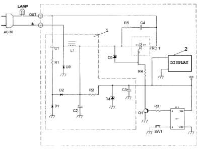
Figure 3
[Technical fields]
The present invention is "a power supply circuit for wall-mounted electronic
switches"
that enables the power supply for control circuit in wall-mounted electronic
switches is
realized space saving, high supply current, low cost, and high quality.
Because an ordinary
wall switch wire uses only one of the two AC power supply lines, which connect
the
objects like lamp on and off, as in Figure 1, we used a separate transistor to
drive out the
current for internal circuitry of wall-mounted electronic switches as in
Figure 2. However,
in case the load [Lamp] is under 20W, current obtainable from the secondary
side of
transformer [TI] is only several mA. In order to raise it to tens of mA, the
size of
transformer [Ti] should be very large and thus it was difficult to use the
circuit as the
power supply of switches that require high current. In addition, a
conventional power
supply circuit as in Figure 2 was unstable in reliability because of its
considerable variation
of supply voltage due to the change of load [Lamp] and its use of big
transformer cause big
- 1 -
CA 02651477 2008-11-06
WO 2007/136178 PCT/KR2007/002143
size and relatively higher cost.
[Background Technology]
Designed to solve these problems, the present invention purposes to provide a
power
25 supply circuit that can supply high power of DC 5V and over 30mA stably
through one line
of wall switch wire under low load [Lamp] of 20W.
[Disclosure of the Invention]
For this purpose, the characteristic of the invented "power supply circuit for
wall-
30 mounted electronic switches" is the inclusion of a step that uses a large
part (30-40%) of
load current for driving the circuit when the load [Lamp] is on. Accordingly,
using the
invented "power supply circuit for wall-mounted electronic switches," we can
use a large
part of load [Lamp] current as power for driving the circuit without a
separate transformer
for driving current out, and this simplifies the circuit, improves space
utility, stabilizes the
35 reliability of power supply, and contributes to price competitiveness.
The following is detailed explanation about desirable applications of the
invented "power
supply circuit for wall-mounted electronic switches" refer to attached
drawings.
Figure 1 is an application circuit example for wall-mounted mechanical
switches. Figure 2
is an application circuit example of a wall-mounted electronic switch using a
conventional
40 power supply circuit. In the application, because the voltage of power for
driving the
- 2 -
CA 02651477 2008-11-06
WO 2007/136178 PCT/KR2007/002143
circuit is very low as 5V and 5mA, the circuit is not applicable to multi-
functional switches
of 5V and over 30mA that use even LCD backlight. The operating principal of
this
invention shall be explained refer to the representative circuit of this
invention, Fig3. In
Figure 3, the switch element that turns on and off the lamp [Lamp] is a triac
[TRC1], and
45 on-off is controlled by a microcomputer(micom) [U1] receiving switch input
[SWI] signal.
Because the charged energy in capacitor C2 is supplied to control micom [U1]
and LCD
driving circuit block [2] through resistor [R2], the circuit configuration of
this invention is
to charge as much current as possible to capacitor [C2].
When the triac [TRC1] is off, the second capacitor [C2] is charged when the AC
in terminal
50 [IN] is higher than the out terminal [OUT], and the charging current path
is as follows:
IN terminal -> Ll -> C2 --> D1 ~ Rl -~ C1
OUT terminal
55 In this time, electric energy is charged to [C1] also, and this electric
energy is discharged
during the next half-wave period [when the voltage of the out terminal is
higher than the
voltage of the in terminal and at that time the discharging current path of
[C1] is as follows:
OUT terminal --> C1 -~ Rl --> D2 --> L 1
60 IN terminal
- 3 -
CA 02651477 2008-11-06
WO 2007/136178 PCT/KR2007/002143
As a matter of fact, the electric energy is supplied to [C2] only during the
half-wave period.
When the lamp switch element [TRC1] is on, it is the same as a short circuit
between the in
terminal [IN] and the out terminal [OUT] above and as a result, current (or
electric charge)
cannot be supplied to the second capacitor [C2] through the current path
above. Thus, the
65 first coil [Ll] is added between the in terminal [IN] and the triac [TRC1],
and the diode
[D3] is added between the ground point and in terminal [IN]. With this
addition, when
load [Lamp] is on, a large part of load current flows charging the second
capacitor [C2] and
the remaining flows through the first coil [LI]. When load is on, if the
voltage of the out
terminal [OUT] is higher than the voltage of the in terminal [IN], the second
capacitor [C2]
70 is charged and at that time the charging current path is as follows.
OUT terminal ~ TRC1 C2 -~i D3
IN terminal
Where, if we assume that the lamp load current is I(t) and the current
charging [C2] is i(t),
the current of Ll becomes l(t) - i(t) and as a result, assuming that the
capacitance of [C2] is
C and the inductance of [L1] is L, charging is done with satisfying the
equation below.
- 4 -
CA 02651477 2008-11-06
WO 2007/136178 PCT/KR2007/002143
d [ I(t) - i(t) ]
L = 0.7 + 1 = f i(t)dt
c
dt
85 As shown in the equation above, when load current [I(t)] is fixed, current
i(t) for driving
can be raised by increasing the inductance of L1.
When the voltage of the in terminal is higher than the voltage of the out
terminal, [C2] is
not charged and the current path of load current [I(t)] is as follows:
90 IN terminal --> L 1---> TRC 1
OUT terminal
As a result, load current flows only through Ll.
95 In the application example of Figure 3, the fourth (Zener) diode is to
supply constant
voltage, the fifth (Zener) diode is for protecting the withstand voltage of
the triac [TRC1],
and the fifth resistor [R5] and the fourth capacitor [C4] are for protecting
the triac [TRC1]
in turning on/off inductive load like a conventional fluorescent lamp using
choke coil.
100
- 5 -
CA 02651477 2008-11-06
WO 2007/136178 PCT/KR2007/002143
[Brief Description of Drawings]
Figure 1: Mechanical wall switch
Figure 2: Drawing of an application circuit example of a wall-mounted
electronic
switch using conventional power supply circuit
105 Figure 3: Drawing of an application circuit example of a wall-mounted
electronic
switch using the invented power supply circuit for wall-mounted electronic
switches
< Description about symbolic marks of the drawings >
110 AC: AC power
LAMP: Lamp
OUT: Switch output terminal
IN: Switch input terminal
1: Power supply circuit block
115 2: LCD driving circuit block
U1: Control micom
TRC1: Triac
Rl - R5: First - fifth resistor
C1 - C4: First - fourth capacitor
120 D 1- D3: First - third diode
- 6 -
CA 02651477 2008-11-06
WO 2007/136178 PCT/KR2007/002143
D4 - D5: Fourth - fifth (Zener) diode
Q 1: First transistor
SWI: Touch switch
VDD: power terminal of DC power supply to the control micom
125 Vss: Control micom grounding terminal
01: Output terminal for on/off control of the triac of the control micom
I1: on/off switch Input terminal of control micom
[Best mode for carrying the Invention]
130 As explained above, the invented "power supply circuit for wall-mounted
electronic
switches" simplifies the structure of power supply circuit for multi-
functional power
supply switches demanding a high driving current, stabilizes the operation of
power supply
circuit, improves the space utility of switches, and price competitiveness.
Fig 3 shows
some desirable application examples, but the invention is not limited to this
example and
135 can be modified in various ways without changing the scope of this
invention, and such
modifications are within the application scope of this invention.
140
- 7 -