Note: Descriptions are shown in the official language in which they were submitted.
CA 02652083 2009-01-23
1
CDMA SYSTEM WHICH USES PRE-ROTATION BEFORE TRANSMISSION
BACKGROUND
This application is a division of Canadian Patent Application Serial Number
2,404,917 filed internationally on March 28, 2001, and entered nationally in
Canada on
September 25, 2002.
The present invention relates generally to digital communications. More
specifically,
the invention relates to a system and method for pre-rotating a digital spread
spectrum signal
prior to transmission in order to improve receiver accuracy and recovery of
the phase and
frequency information by the receiver.
Many current communication systems use digital spread spectrum modulation or
code
divisional multiple access (CDMA) technology. Digital spread spectrum is a
communication
technique in which data is transmitted with a broadened band (spread spectrum)
by modulating
the data to be transmitted with a pseudo-noise signal. CDMA can transmit data
without being
affected by signal distortion or an interfering frequency in the transmission
path.
Shown in Figure 1 is a simplified CDMA communication system that involves a
single
communication channel of a given bandwidth which is mixed by a spreading code
which
repeats a predetermined pattern generated by a pseudo-noise (pn) sequence
generator. A data
signal is modulated with the pn sequence to produce digital spread spectrum
signal. A carrier
signal is modulated with the digital spread spectrum signal to establish a
forward link and is
then transmitted. A receiver demodulates the transmission to extract the
digital spread
spectrum signal. The same process is repeated to establish a reverse link.
During terrestrial communication, a transmitted signal is typically disturbed
by
reflections due to varying terrain and environmental conditions and man-made
obstructions.
Thus, a single transmitted signal produces a plurality of received signals
with differing time
delays at the receiver, an effect which is commonly known as multipath
distortion. During
multipath distortion, the signal from each different path arrives delayed at
the receiver with a
unique amplitude and carrier phase.
CA 02652083 2009-01-23
2
U.S. Patent No. 5,659,573 discloses a system in which the error associated
with
multipath distortion is typically corrected at the receiver after the signal
has been correlated
with the matching pn sequence and the transmitted data has been reproduced.
Thus, the
correlation is completed with error incorporated in the signal. Similar
multipath distortion
affects the reverse link transmission.
French Patent No. 2767238 discloses a system for estimating a received signal
in which
a phase shift of the received signal is estimated by applying a predetermined
function. The
phase shift is used in a phase-locked loop so that the system converges
towards a null error.
European Patent No. 0818892 and U.S. Patent No. 5,499,236 disclose systems in
which a base station sends an error signal within the downlink transmission
indicating an
adjustment to be made by the terminal station for reverse link transmission.
Accordingly, there exists a need for a system that corrects a signal for
errors
encountered during transmission.
SUMMARY
The present invention relates to a digital spread spectrum communication
system
that calculates phase and frequency error on a received signal from a
communicating entity
during a wireless communication and pre-corrects a signal for phase and
frequency error
prior to transmission to that entity.
Accordingly, the invention comprises a wireless transmitter comprising: an
input
configured to receive a data signal; a mixer for mixing the data signal with a
correction signal
producing a corrected signal, the correction signal changing a phase in the
data signal to
compensate for a measured phase error at a desired receiver; a modulator for
modulating the
corrected signal to radio frequency as a radio frequency signal; and an
antenna for radiating the
radio frequency signal.
The invention further comprises a base station comprising: an input configured
to
receive a data signal; a mixer for mixing the data signal with a correction
signal producing a
corrected signal, the correction signal changing a phase in the data signal to
compensate for a
measured phase error at a desired receiver; a modulator for modulating the
corrected signal to
CA 02652083 2009-01-23
3
radio frequency as a radio frequency signal; and an antenna for radiating the
radio frequency
signal.
The invention still further comprises a mobile station comprising: an input
configured
to receive a data signal; a mixer for mixing the data signal with a correction
signal producing a
corrected signal, the correction signal changing a phase in the data signal to
compensate for a
measured phase error at a desired receiver; a modulator for modulating the
corrected signal to
radio frequency as a radio frequency signal; and
an antenna for radiating the radio frequency signal.
BRIEF DESCRIPTION OF THE DRAWING(S)
Figure 1 is a simplified block diagram of a prior art CDMA communication
system.
Figure 2 is a detailed block diagram of a B-CDMAJ communication system.
Figure 3A is a detailed block diagram of the present invention using one
pseudo-pilot
signal, with carrier-offset correction implemented at the chip level.
Figure 3B is a block diagram of a rake receiver.
Figure 4 is a diagram of a received symbol po on the QPSK constellation
showing a
hard decision.
Figure 5 is a diagram of the angle of correction corresponding to the assigned
symbol.
Figure 6 is a diagram of the resultant symbol error after applying the
correction
corresponding to the assigned symbol.
Figure 7 is a block diagram of a conventional phase-locked loop.
Figure 8A is a simple block diagram of a transmitter in accordance with the
preferred
embodiment of the present invention.
Figure 8B is a simple block diagram of a transmitter in accordance with an
alternative
embodiment of the present invention.
Figure 8C is a simple block diagram of a transmitter in accordance with an
alternative
embodiment of the present invention.
CA 02652083 2009-01-23
4
DETAILED DESCRIPTION OF THE PREFERRED EMBODIMENTS
The preferred embodiment will be described with reference to the drawing
figures
where like numerals represent like elements throughout.
A CDMA communication system 25 as shown in Figure 2 includes a transmitter 27
and a receiver 29, which may reside in either a base station or a mobile user
receiver. The
transmitter 27 includes a signal processor 31 which encodes voice and nonvoice
signals 33
into data at various rates, e.g. data rates of 8 kbps, 16 kbps, 32 kbps, or 64
kbps. The signal
processor 31 selects a specific data rate depending upon the type of signal,
or in response to a
set data rate.
By way of background, two steps are involved in the generation of a
transmitted signal
in a multiple access environment. First, the input data 33 which can be
considered a bi-phase
modulated signal is encoded using forward error-correction (FEC) coding 35.
For example, if
a R=2 convolution code is used, the single bi-phase modulated data signal
becomes bivariate
or two bi-phase modulated signals. One signal is designated the in-phase (I)
channe141 a. The
other signal is designated the quadrature (Q) channe141b. A complex number is
in the form
a+bj, where a and b are real numbers and j2=-1. Bi-phase modulated I and Q
signals are
usually referred to as quadrature phase shift keying (QPSK). In the preferred
embodiment, the
tap generator polynomials for a constraint length of K=7 and a convolutional
code rate of R=2
are G1=1718 37 and G2=1338 39.
In the second step, the two bi-phase modulated data or symbols 41a, 41b are
spread
with a complex pseudo-noise (pn) sequence. The resulting I 45a and Q 45b
spread signals are
combined 53 with other spread signals (channels) having different spreading
codes, mixed
with a carrier signal 51 and then transmitted 55. The transmission 55 may
contain a plurality
of individual channels having different data rates.
The receiver 29 includes a demodulator 57a, 57b which downconverts the
transmitted
broadband signal 55 into an intermediate frequency signal 59a, 59b. A second
downconversion reduces the signal to baseband. The QPSK signal is then
filtered 61 and
mixed 63a, 63b with the locally generated complex pn sequence 43a, 43b which
matches the
conjugate of the transmitted complex code. Only the original waveforms which
were spread
CA 02652083 2009-01-23
by the same code at the transmitter 27 will be effectively despread. Others
will appear as noise
to the receiver 29. The data 65a, 65b is then passed onto a signal processor
67 where FEC
decoding is performed on the convolutionally encoded data.
When the signal is received and demodulated, the baseband signal is at the
chip level.
5 Both the I and Q components of the signal are despread using the conjugate
of the pn sequence
used during spreading, returning the signal to the symbol level. However, due
to carrier offset,
phase corruption experienced during transmission manifests itself by
distorting the individual
chip waveforms. If carrier offset correction is performed at the chip level
overall accuracy
increases due to the inherent resolution of the chip-level signal. Carrier
offset correction may
also be performed at the symbol level but with less overall accuracy. However,
since the
syinbol rate is much less than the chip rate, a lower overall processing speed
is required when
the correction is done at the symbol level.
As shown in Figure 3A, a receiver using the system 75 and method of the
present
invention is shown. A complex baseband digital spread spectrum signal 77
comprised of in-
phase and quadrature phase components is input and filtered using an adaptive
matched filter
(AMF) 79 or other adaptive filtering means. The AMF 79 is a transversal filter
(finite impulse
response) which uses filter coefficients 81 to overlay delayed replicas of the
received signal 77
onto each other to provide a filtered signal output 83 having an increased
signal-to-noise ratio
(SNR). The output 83 of the AMF 79 is coupled to a plurality of channel
despreaders 851, 852,
85õ and a pilot despreader 87. The pilot signal 89 is despread with a separate
despreader 87
and pn sequence 91 contemporaneous with the transmitted data 77 assigned to
channels which
are despread 851, 852, 85õ with pn sequences 931, 932, 93õ of their own. After
the data
channels are despread 85 1, 852, 85,,, the data bit streams 95 1, 952, 95n are
coupled to Viterbi
decoders 971, 972, 97n and output 99 i, 992, 99,,.
The filter coefficients 81, or weights, used in adjusting the AMF 79 are
obtained by the
demodulation of the individual multipath propagation paths. This operation is
perfonned by a
rake receiver 101. The use of a rake receiver 101 to compensate for multipath
distortion is
well known to those skilled in the communication arts.
As shown in Figure 3B, the rake receiver 101 consists of a parallel
combination of path
demodulators Afingers@ 1030, 1031, 1032, 103õ which demodulate a particular
multipath
component. The pilot sequence tracking loop of a particular demodulator is
initiated by the
CA 02652083 2009-01-23
6
timing estimation of a given path as determined by a pn sequence 105. In the
prior art, a pilot
signal is used for despreading the individual signals of the rake. In the
present invention, the
pn sequence 105 may belong to any channe193, of the communication system.
Typically, the
channel with the largest received signal is used.
Each path demodulator includes a complex mixer 107o, 1071, 1072, 107,,, and
summer
and latch 1090, 1091, 1092, 109n. For each rake element, the pn sequence 105
is delayed i
1111, 1112, 111õ by one chip and mixed 107 i, 1072, 107n with the baseband
spread spectrum
signal 113 thereby despreading each signal. Each multiplication product is
input into an
accumulator 1090, 1091, 1092, 109n where it is added to the previous product
and latched out
after the next symbol-clock cycle. The rake receiver 101 provides relative
path values for each
multipath component. The plurality of n-dimension outputs 115o, 1151, 1152,
115n provide
estimates of the sampled channel impulse response that contain a relative
phase error of either
OE, 90E, 180E, or 270E.
Referring back to Figure 3A, the plurality of outputs from the rake receiver
are coupled
to an n-dimensional complex mixer 117. Mixed with each rake receiver 101
output 115 is a
correction to remove the relative phase error contained in the rake output.
A pilot signal is also a complex QPSK signal, but with the quadrature
component set at
zero. The error correction 119 signal of the present invention is derived from
the despread
channel 95, by first performing a hard decision 121 on each of the sylnbols of
the despread
signa1951. A hard decision processor 121 determines the QPSK constellation
position that is
closest to the despread symbol value.
As shown in Figure 4, the Euclidean distance processor compares a received
symbol po
of channel 1 to the four QPSK constellation points xi, i, x_i, i, x_i, _1, xi,
_1. It is necessary to
examine each received symbol po due to corruption during transmission 55 by
noise and
distortion, whether multipath or radio frequency. The hard decision processor
121 computes
the four distances dl, d2, d3, d4 to each quadrant from the received symbol po
and chooses the
shortest distance dz and assigns that symbol location x_i, 1. The original
symbol coordinates po
are discarded.
Referring back to Figure 3A, after undergoing each hard symbol decision 121,
the
complex conjugates 123 for each symbol output 125 are determined. A complex
conjugate is
CA 02652083 2009-01-23
7
one of a pair of complex numbers with identical real parts and with imaginary
parts differing
only in sign. As shown in Figure 5, a symbol is demodulated or de-rotated by
first determining
the complex conjugate of the assigned symbol coordinates x_1, _1, forming the
correction signal
119 which is used to remove the relative phase error contained in the rake
output. Thus, the
rake output is effectively de-rotated by the angle associated with the hard
decision, removing
the relative phase error. This operation effectively provides a rake that is
driven by a pilot
signal, but without an absolute phase reference.
Referring back to Figure 3A, the output 119 from the complex conjugate 123 is
coupled to a complex n-dimensional mixer 117 where each output of the rake
receiver 101 is
mixed with the correction signal 119. The resulting products 127 are noisy
estimates of the
channel impulse response pl as shown in Figure 6. The error shown in Figure 6
is indicated by
a radian distance of 7E/6 from the in-phase axis.
Referring back to Figure 3A, the outputs 115 of the complex n-dimensional
channel
mixer 117 are coupled to an n-dimensional estimator 131. The channel estimator
131 is a
plurality of low-pass filters, each for filtering a multipath component. The
outputs 81 of the n-
dimensional estimator 131 are coupled to the AMF 79. These outputs 81 act as
the AMF 79
filter weights. The AMF 79 filters the baseband signal to compensate for
channel distortion
due to multipath without requiring a large magnitude pilot signal.
The rake receiver 101 is used in conjunction with the phase-locked loop (PLL)
133
circuits to remove carrier offset. Carrier offset occurs as a result of
transmitter/receiver
component mismatches and other RF distortion. The present invention 75 uses a
low level
pilot signal 135 which is produced by despreading 87 the pilot from the
baseband signal 77
with a pilot pn sequence 91. The pilot signal is coupled to a single input PLL
133, shown in
Figure 7. The PLL 133 measures the phase difference between the pilot signal
135 and a
reference phase of 0. The despread pilot signal 135 is the actual error signal
coupled to the
PLL 133.
The PLL 133 includes an arctangent analyzer 136, complex filter 137, an
integrator 139
and a phase-to-complex-number converter 141. The pilot signal 135 is the error
signal input to
the PLL 133 and is coupled to the complex filter 137. The complex filter 137
includes two
gain stages, an integrator 145 and a summer 147. The output from the complex
filter 137 is
coupled to the integrator 139. The integral of frequency is phase, which is
output 140 to the
CA 02652083 2009-01-23
8
converter 141. The phase output 140 is coupled to a converter 141 which
converts the phase
signal into a complex signal for mixing 151 with the baseband signa177. Since
the upstream
operations are commutative, the output 149 of the PLL 133 is also the feedback
loop into the
system 75.
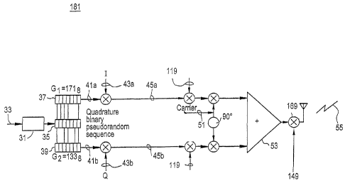
The correction signal 119 of the complex conjugate 123 and the output signal
149 of
the PLL 133 are each coupled to mixers located within the transmitter 181, in
order to correct
the signal before transmission as shown in Figure 8A. The transmitter 181
shown in Figure
8A operates in a similar manner to the transmitter 27 shown in Figure 2,
except that the signal
ready for transmission is pre-rotated prior to transmission. Referring to
Figure 8A, data 164i,
1642, 1643 is encoded using forward correcting coding (FEC) 35. The two bi-
phase modulated
data or symbols 41a, 41b are spread with a complex pseudo-noise (pn) sequence
and the
resulting I 45a and Q 45b spread signals are mixed with the correction signal
119, upconverted
with the carrier signal 51, and combined 53 with other spread signals having
different
spreading codes. The resulting signal 55 is again corrected using the signal
149 from the
receiver PLL 133. The signa156 which has been pre-corrected for phase and
frequency is then
transmitted. In this manner, the present invention utilizes the signals 119,
149 generated by
the receiver 71 to pre-correct the transmitted signal and reduce the phase and
frequency errors
in the signals as received at the receiving unit.
Referring to Figure 8B, a transmitter 183 made in accordance with an
alternative
embodiment of the present invention is shown. This embodiment is similar to
the embodiment
shown in Figure 8A, except that the correction signal 119 is mixed with the
baseband data
signal via a mixer 157. Thus, the baseband data is pre-corrected prior to
encoding and
spreading. Of course, those of skill in the art should realize that other
processing steps may be
introduced before the correction signal 119 is mixed with the data signal.
Referring to Figure 8C, a transmitter 188 made in accordance with another
alternative
embodiment of the present invention is shown. In this embodiment, the
correction signal 119
and the carrier offset signal 149 are input into a combiner, which combines
the signal into a
single pre-correction signal, and mixed using the mixer 169 with the output of
the summer 53
prior to transmission.
Finally, it should be noted that the carrier offset correction and the pre-
rotation
correction are separate corrections. Each may be utilized independently of the
other. For
CA 02652083 2009-01-23
9
example, the system may pre-correct only for carrier offset error and may not
perfonn pre-
rotation. Alternatively, the system may perform pre-rotation but may not
correct for carrier
offset error.
While specific embodiments of the present invention have been shown and
described,
many modifications and variations could be made by one skilled in the art
without departing
from the spirit and scope of the invention. The above description serves to
illustrate and not
limit the particular form in any way.