Note: Descriptions are shown in the official language in which they were submitted.
CA 02652436 2008-11-17
WO 2007/131360 PCT/CA2007/000865
1 LAMINAR FLOW WELL
2
3 TECHNICAL FIELD
4 [0001] The following relates to soldering and has particular utility in
solder fountain flow
wells used in pin through hole (PTH) rework processes.
6 BACKGROUND
7 [0002] Many electronic components, e.g. connectors, have a series of
protruding pins that
8 are used to connect such components to a printed circuit board (PCB) by way
of pin through
9 hole (PTH) barrels installed in the PCB. PTH barrels are generally "spool"
shaped and
include an annular sleeve defining a central aperture which extends through
the thickness of
11 the PCB and an upper and lower annular ring attached to the sleeve that
extend over a portion
12 of the upper and lower surfaces of the PCB in the vicinity of the sleeve.
The interface of the
13 rings and the sleeves of a PTH barrel is often referred to as a barrel
"knee". The PTH barrels
14 are typically made from copper.
[0003] To attach the component to the PCB, the pins are aligned with
respective PTH
16 barrels, the pins are fed through the central apertures defined by the
respective barrels, and
17 the pins are then soldered to the barrels as is well known in the art. In
order to decrease the
18 time in soldering the pins, a wave solder machine may be used to effect the
primary
19 attachment of the component to the PCB. Often, however, certain ones of the
solder joints
require reworking and undergo a rework process. Reworking the solder joints
can be
21 accomplished using a solder fountain.
22 [0004] A solder fountain includes a solder pot that contains a quantity of
molten solder
23 and a pump for pumping the molten solder up through a flow well which
provides a wave of
24 liquid solder that is used to rework the solder joints of the PTH barrels.
Unused solder is re-
circulated to the solder pot using a spill mechanism. The pump is typically
adjustable such
26 that the flow rate of the solder can be controlled. The temperature of the
molten solder can
27 also be controlled in order for the solder in the solder wave to attain a
particular temperature.
28 [0005] As is well know in the art, solder is a fusible metal alloy, often
made of tin and
29 lead, which is melted to join metallic surfaces. The use of lead in general
has become
increasingly undesirable, leading to much interest in lead-free solders. Such
lead-free solders
31 contain tin, copper, silver, and sometimes bismuth, indium, zinc, and other
metals in varying
21640427.1
- 1 -
CA 02652436 2008-11-17
WO 2007/131360 PCT/CA2007/000865
1 amounts. The lead-free replacements for conventional solder have higher
melting points, and
2 often this leads to the need to re-engineer some components and materials
used in electronic
3 assemblies such as PCBs. Lead-free solder joints may produce mechanically
weaker joints
4 depending on service and manufacture conditions, which may lead to a
decrease in reliability
using such solders.
6 [0006] Of particular concern in PTH rework applications is copper (Cu)
dissolution. Cu
7 dissolution often occurs when the Cu rings of the PTH barrels come into
contact with the
8 molten solder alloy during the rework process. Cu dissolution results in a
deterioration of the
9 barrel such that the ring may become detached from the sleeve or in some
cases be
completely dissolved. The occurrence of Cu dissolution is not only prevalent
in lead-free
11 solder a] loys, but also eutectic leaded solder alloys, although generally
to a lesser extent. The
12 combined change in alloy composition and corresponding higher melting point
of the lead-
13 free solder requires that the molten solder maintain a higher operating
temperature, thus often
14 accelerating the rate and consequently the extent of Cu dissolution. The
barrel knee is
typically the most vulnerable to Cu dissolution. As a result, the acceptable
contact time for
16 lead-free solder is generally much lower than for leaded solder. For
example, studies have
17 shown that a copper barrel knee can only withstand approximately 30 seconds
of contact time
18 using SAC405 lead-free alloy, whereas a copper barrel knee exposed to
leaded solders is
19 known, in many situations, to be able to withstand approximately 60-90
seconds of contact
time before complete dissolution of the knee occurs on the same test vehicle.
21 [0007] It is therefore an object of the following to obviate or mitigate
the above-
22 mentioned disadvantages.
23 SUMMARY
24 [00081 It has been observed that turbulent solder flow, particularly at the
opening of a
conventional flow well, correlates to a greater degree of Cu dissolution of
the PTH barrels of
26 a PCB, especially those that are aligned with the opening. A more laminar
solder flow can
27 be produced to more evenly distribute the solder flow and thus reduce the
rate of Cu
28 dissolution near the flow well opening, particularly during a PTH rework
process.
29 100091 In one aspect, a flow well for a solder fountain is provided
comprising an opening
for receiving a flow of solder from the solder fountain; an open face for
providing a surface
21640427.1
-2-
CA 02652436 2008-11-17
WO 2007/131360 PCT/CA2007/000865
I of solder; and a flow distribution element between the opening and the
surface, the flow
2 distribution element being configured to redirect solder flow away from the
opening.
3 [0010] In another aspect, there is provided a flow distribution element for
a flow well
4 comprising a member for directing solder flow away from an opening in the
flow well and an
attachment mechanism for securing the flow distribution element over the
opening.
6 [0011] In yet another aspect, there is provided a method for soldering a
circuit board
7 using a solder fountain comprising providing a flow well having an opening,
an open face
8 and a flow distribution element between the opening and the open face;
feeding solder into
9 the flow well; redirecting the solder away from the opening using the flow
distribution
element; and providing a surface of solder at the open face.
11 BRIEF DESCRIPTION OF THE DRAWINGS
12 [0012] An embodiment of the invention will now be described by way of
example only
13 with reference to the appended drawings wherein:
14 [0013] Figure 1 is a perspective view of a solder fountain machine.
[0014] Figure 2 is an elevation view of the flow well shown in Figure 1
showing a PCB
16 in cross section.
17 100151 Figure 3A is an enlarged sectional view of the PCB of Figure 2 prior
to pin
18 insertion.
19 [0016] Figure 3B is an enlarged sectional view of the PCB of Figure 2
following pin
insertion and soldering.
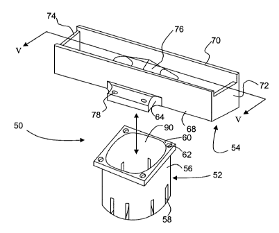
21 100171 Figure 4 is an exploded perspective view of a laminar flow well.
22 [0018] Figure 5 is a sectional view of the flow well shown in Figure 4
along the live V-V.
23 [0019] Figure 6 is a top view of the flow well shown in Figure 4.
24 [00201 Figure 7 is a bottom view of the flow well base shown in Figure 4.
21640427.1
-3-
CA 02652436 2008-11-17
WO 2007/131360 PCT/CA2007/000865
1 [0021] Figure 8 is an enlarged photograph showing the effects of Cu
dissolution using a
2 conventional flow well.
3 [0022] Figure 9 is an enlarged photograph showing the effects of Cu
dissolution using the
4 flow well shown in Figure 4.
[0023] Figure 10 is a graph illustrating Cu dissolution rate for turbulent and
laminar
6 solder flow.
7 [0024] Figure 11 is a chart comparing average Cu thickness for turbulent and
laminar
8 solder flow at the center of the connector shown in Figure 2.
9 [0025] Figure 12 is a chart comparing average Cu thickness for turbulent and
laminar
solder flow at one edge of the connector shown in Figure 2.
11 [0026] Figure 13 is a chart comparing average Cu thickness for turbulent
and laminar
12 solder flow at the edge nearer to the longitudinal centerline of the
connector shown in Figure
13 2.
14 [0027] Figure 14 is a perspective view of another embodiment.
[0028] Figure 15 is a sectional view along the line XV-XV of Figure 14 of yet
another
16 embodiment.
17 DETAILED DESCRIPTION OF THE DRAWINGS
18 [0029] Referring therefore to Figure 1, a solder fountain machine is
generally denoted by
19 numeral 10. The solder fountain 10 has a base 12 supporting a protective
housing 14. The
housing 14 surrounds a solder pot 16 containing a quantity of molten solder
18. A flow well
21 20 extends upwardly from the solder pot 16. A pump 22 contained in the
solder pot 16
22 pumps the molten solder 18 through the flow well 20 creating a solder wave
24. The fountain
23 10 also includes a control box 26 that is used to control the operation of
the solder fountain
24 10, e.g., the flow rate of the pump. The solder wave 24 spills over and
returns to the solder
pot 16 via an inverted frustum 28 with a central aperture 29 that covers the
solder pot 16.
26 [0030] As best seen in Figure 2, a PCB 30 has a series of copper PTH
barrels 32 that are
27 aligned on the board 30 and correspond to the arrangement of a series of
pins 34 extending
21640427.1
-4-
CA 02652436 2008-11-17
WO 2007/131360 PCT/CA2007/000865
1 from a connector 36. A exemplary barrel 32 is shown in section in Figure 3A
prior to pin
2 insertion. The barrel 32 comprises an annular sleeve 38, a lower annular
ring 40 and an
3 upper annular ring 42. The interface of the lower ring 40 and the sleeve 38
defines a left
4 barrel knee 46 and a right barrel knee 44. As shown in Figure 3B, the solder
wave 24,
coming into contact with the barrels 32 when the pins 34 are fed through
respective ones of
6 the barrels 32, will effectively solder the connector 36 to the PCB 30 to
create a solder joint
7 48.
8 [0031] In electronics manufacturing, in particular Electronics Manufacturing
Services
9 (EMS), there is often a need to repair/rework defective PTH connectors 36
which are
soldered to a PCB 30. In order to repair/rework the defective connectors 36, a
solder fountain
11 30 (or "mini pot") is used. The solder fountain 10 reworks a PTH connector
36 by pumping a
12 small amount of molten solder 18 through the flow well 20 to create a
solder wave 24 as
13 explained above. The flow wel120 is sized to substantially correspond to
the dimensions of
14 the connector 36 being reworked as best seen in Figure 2.
[0032] Once a solder fountain 10 rework process has been initiated on a PCB
30, there is
16 typically a fixed number of solder cycles that can be performed on the PCB
before the board
17 is irreparably damaged, i.e., each solder cycle increases the risk of
damage to the PTH barrels
18 32 and the laminate board 30 itself. Therefore, it is desirable to perform
the rework in the
19 fewest number of solder cycles as possible. If the PCB 30 is exposed to
molten solder 18 for
a relatively large amount of cumulative contact time (e.g. 90+ seconds for
leaded alloys and
21 approximately 30+ seconds for lead-free alloys), the PCB 30 may be
irreparable at the time of
22 rework or if a rework is required years later. Cu dissolution often occurs
due to such
23 prolonged contact time.
24 [0033] It has been observed, when using a conventional flow well (not
shown), that
barrels 32 located near the center of the connector 36 being reworked exhibit
a higher degree
26 of Cu dissolution (and thus damage) at the knees 44, 46 of the barre132
when compared to
27 the barrels 32 located nearer the outer edges of the same connector 36.
28 100341 A conventional flow well that has been traditionally used with a
solder fountain
29 10 uses a single circular or oval opening for pumping molten solder 18 from
the solder pot 16
to the flow well base. The solder makes direct contact with the PCB 30
undergoing the
21640427.1
-5-
CA 02652436 2008-11-17
WO 2007/131360 PCT/CA2007/000865
1 rework process and spills over the two ends of the flow well. It was
determined that such
2 flow of solder from a single opening correlates to a higher flow rate of
solder (and thus a
3 turbulent solder flow), which in turn correlates to a higher degree of Cu
dissolution at the
4 "central" PTH barrels 32, the effects of which are explained in greater
detail below. The
central barrels 32 are positioned immediately above the opening and, as such,
can experience
6 approximately 100% of the flow of molten solder as it spreads out to create
the solder wave
7 24.
8 [0035] In order to lessen the Cu dissolution at the central portions of the
connector 36, it
9 was determined, based on the identification of the above correlation, that a
more laminar flow
of molten solder to the flow well should be used. In order to minimize
turbulent solder flow
11 and create a laminar solder flow, a flow distribution element (e.g. baffle,
diffuser etc.) is used
12 to distribute the solder flow before it makes contact with the PCB 30.
13 [0036] In a preferred embodiment, shown in Figures 4 -7, the single opening
feeding
14 molten solder to the flow well in a solder fountain 10 is modified to
provide a plurality of
openings in order to redirect or baffle the solder flow away from or about the
opening. The
16 multiple openings are configured to change the substantially vertical
direction of solder flow
17 from the single opening into a more horizontal and thus laminar flow
vector, to distribute the
18 force of the solder 18 before making contact with the barrels 32 and PCB
30. The overall
19 solder flow is consequently more laminar, which has been shown to reduce
the degree of Cu
dissolution as will be explained in greater detail below.
21 [0037] Referring now to Figure 4, a flow well 50 for producing a more
laminar solder
22 flow comprises an adapter 52 for connecting the flow well 50 to the outlet
(not shown) of the
23 pump 22, and a base 54 for providing the solder wave 24.
24 100381 The adapter 52 includes a slotted sleeve 56 that is sized and shaped
to fit over the
outlet of the pump 22. The sleeve 56 includes a series of slots 58 to allow a
snug fitment of
26 the adapter 52 over the end of the outlet. The adapter 52 also includes a
flange 60 at the end
27 opposite that having the slots 58. The flange 60 includes a series of holes
62 for attaching the
28 adapter 52 to the base 54 and defines an opening 90 to permit the flow of
solder 18 to the
29 base 54.
21640427.1
-6-
CA 02652436 2008-11-17
WO 2007/131360 PCT/CA2007/000865
1 [0039] The base 54 has a pair of side walls 68, 70 separated by a pair of
end walls 72, 74
2 at respective ends. The end walls 72 74 have a height that is less than the
height of the side
3 walls 68, 70 to allow for solder to spill over the base 54 and re-circulate
to the solder pot 16.
4 The sidewall 68 has a first flange 64 extending from its mid-portion and the
sidewall 70 has a
second flange 66 extending from its mid-portion. Aligned with the flanges 64,
66 is a baffle
6 member 76 formed in the floor of the base 54 to provide a flow distribution
element. The
7 baffle member 76 directs solder flowing through the adapter 52 towards each
end of the base
8 54 using a pair of inclined passages 84, 86. A first floor portion 80 slopes
inwardly from the
9 end wall 74 towards the inclined passage 84 and a second floor portion 82
slopes inwardly
from the end wall 72 towards the inclined passage 86. The flanges 62, 66
include a series of
11 holes 78. The holes 78 are aligned with the holes 62 on the adapter 52 in
order to allow the
12 adapter 52 to be attached to the base 54.
13 100401 The lower ends of the inclined passages 84, 86 are adjacent and
diverge from each
14 other such that their upper ends emerge on opposite sides of the baffle
member 76. The
lower ends of the passages 84, 86 are positioned over the opening 90. As a
result, solder
16 flowing through the opening 90 is directed in either direction around the
baffle member 76 in
17 a more horizontal manner when compared to its direction when emerging from
the opening
18 90 alone. This altered flow results in a more laminar solder flow.
19 [0041] The effects of Cu dissolution during PTH rework was observed and
compared
between a conventional, single opening flow well (not shown) and the flow well
50 shown in
21 Figure 4, which provides a more laminar flow. It was found experimentally,
that the more
22 laminar solder flow rate resulted in a lesser degree of Cu dissolution
overall when compared
23 to a more turbulent solder flow rate from a single opening, in particular
in the vicinity of the
24 opening 90.
[0042] The relatively turbulent flow rate of a conventional flow well was
compared with
26 the more laminar flow rate of the flow well 50 for different contact times.
The constant
27 variables for the molten solder 18 included a solder pot temperature of 265
C and a PCB
28 preheat temperature of 150 C. The contact times used were based on previous
knowledge
29 that a turbulent flow rate will experience Cu dissolution of approximately
100% (complete
dissolution of the barrel knee 44, 46) in approximately 30 seconds. The graph
shown in
31 Figure 10 compares the dissolution rate of the conventional turbulent flow
well (thick line)
21640427.1
-7-
CA 02652436 2008-11-17
WO 2007/131360 PCT/CA2007/000865
I with the expected dissolution rate for the more laminar flow well 50 (thin
line). It has been
2 determined that in many cases, the Cu dissolution rate for a conventional
flow well is
3 approximately 0.030 mils/sec.
4 [0043] In order to determine the effects of Cu dissolution according to the
above
experiment, a cross-section of the PCB 30 was taken to allow examination of
the barrels 32 at
6 both the mid-portion and the ends of the connector 36. The Cu thickness at
the ring 40 and
7 the knees 44, 46 was measured. The initial Cu thickness for the knee of the
barrel 32 is
8 approximately 1.15 mils.
9 [0044] It was found that the more laminar flow rate achieved using the flow
well 50
resulted in an approximate Cu dissolution rate of 0.02 mils/sec, which is
about a 33%
11 improvement over the conventional, more turbulent flow well. The results of
the above are
12 illustrated in the charts shown in Figures 11-13. The following results
used a contact time of
13 between 20 and 25 seconds.
14 [0045] In Figure 11, the average Cu thickness for the laminar and turbulent
flow is
compared for two different connectors on the same board (i.e. C2 and C3). The
16 measurements were taken near the center of the connectors. The average Cu
thickness is
17 determined by averaging the thickness of the left knee 46 and right knee 44
as measured once
18 the board and barrels are in cross-section. For the C2 connector, the
average Cu thickness
19 was approximately 0.80 mils for the flow well 50 and approximately 0.26
mils for the
conventional, more turbulent flow well. For the C3 connector, the average Cu
thickness was
21 approximately 0.88 mils for the flow well 50 and effectively zero (0) mils
for the
22 conventional, more turbulent flow well.
23 [0046] Figure 12 compares the average Cu thickness for laminar and
turbulent flow as
24 measured at the edge of the respective connectors. For the C2 connector,
the average Cu
thickness was approximately 0.78 mils for the flow well 50 and approximately
0.85 mils for
26 the conventional, more turbulent flow well. For the C3 connector, the
average Cu thickness
27 was approximately 0.80 mils for the flow well 50 and approximately 0.86
mils for the
28 conventional, more turbulent flow well.
21640427.1
-8-
CA 02652436 2008-11-17
WO 2007/131360 PCT/CA2007/000865
1 [0047] Figure 13 compares the average Cu thickness measured at the edge of
the
2 respective connectors but near the longitudinal centerline of the connector
and exhibited
3 similar results to those shown in Figure 12.
4 [0048] It will be noted from Figures 11-13 that the conventional flow well
exhibited
slightly less Cu dissolution at the edge of the connectors than did the more
laminar flow well
6 50. This is likely the result of the redirection of the solder flow at the
center of the flow well
7 50 towards the ends of the flow well 50, resulting in a relatively higher
flow rate at the ends
8 of the connector 36.
9 [0049] However, it can be seen that, especially in Figure 11, the more
balanced flow in
the flow well 50 greatly reduces the Cu dissolution at the centre portion of
the connector. As
11 a result, the overall Cu dissolution is more evenly distributed across the
length of the
12 connector when using the flow well 50 even though the Cu dissolution at the
ends of the
13 connector are relatively higher when compared to the conventional flow
well. Such an even
14 distribution inhibits drastic Cu dissolution at the centre of the connector
as shown in Figure
11 where using the conventional, more turbulent flow well, complete
dissolution can occur
16 (e.g. Figure 8 explained below).
17 [0050] The effect of Cu dissolution in a conventional flow well is shown in
Figure 8 and
18 the effect of Cu dissolution in the more laminar flow well 50 is shown in
Figure 9. A
19 complete dissolution of the barrel knee 44 is shown in Figure 8 and a "best
case" result for
the flow well 50 is shown in Figure 9 wherein the Cu thickness is largely
unaffected by the
21 PTH rework process.
22 [0051] In another embodiment shown in Figure 14, a conventional flow well
100 is
23 adapted to include a separate and detachable baffle mechanism or attachment
110 as the flow
24 distribution element used to create a more laminar solder flow. The flow
well 100 includes
an opening 102 for solder to flow through and has an attachment mechanism by
way of a pair
26 of holes 104 for attaching the baffle attachment 110 to the flow well 100.
The baffle
27 attachment 110 is supported by a pair of posts 106, 108 and secured to the
flow well 100
28 using a pair of screws 112 thus positioning the attachment 110 above the
opening 102. As a
29 result, the baffle attachment 110 redirects solder flow to produce a more
horizontal and thus
21640427.1
-9-
CA 02652436 2008-11-17
WO 2007/131360 PCT/CA2007/000865
1 more laminar flow similar to the embodiment described above. This embodiment
is
2 particularly useful for retrofitting existing flow well components.
3 [0052] In yet another embodiment shown in Figure 15, the floor 202 of a
conventional
4 flow wel1200 can be retrofitted to include a flow distribution element
having an attachment
mechanism, e.g. by modifying the flow well 200 to include a pair of holes 204
for securing a
6 perforated plate 212 atop a pair of posts 206. As shown in Figure 15, any
perforation pattern
7 may be used, such as the single row pattern 216 of the plate 212a and the
double row pattern
8 214 of the plate 212b. The solder flowing through the outlet 210 and the
opening 208 is
9 distributed through the perforations to provide a more even and thus more
laminar solder
flow in the flow wel1200.
11 [0053] It will be appreciated that in yet another embodiment (not shown),
the plates 212a,
12 212b may also be used in conjunctions with the embodiment of Figure 4 in
addition to the
13 inclined passages 84, 86.
14 [0054] It has therefore been shown that turbulent solder flow, particularly
at the opening
of a conventional flow well, correlates to a greater degree of Cu dissolution
of the PTH
16 barrels of a PCB, especially those that are substantially aligned with the
opening. By
17 incorporating a flow distribution element such as a baffle or diffuser in a
modified or
18 retrofitted flow well, a more laminar solder flow is created to more evenly
distribute the
19 solder flow and thus reduce the rate of Cu dissolution near the flow well
opening, particularly
during a PTH rework process. It can be seen that existing flow wells can be
retrofitted or
21 custom flow wells can be manufactured to include the flow distribution
element. It can be
22 appreciated that the flow distribution element can comprise any device or
modification of the
23 flow well that, when used, distributes solder in the flow well resulting in
a less turbulent
24 solder flow.
100551 Although the invention has been described with reference to certain
specific
26 embodiments, various modifications thereof will be apparent to those
skilled in the art
27 without departing from the spirit and scope of the invention as outlined in
the claims
28 appended hereto.
21640427.1
-10-