Note: Descriptions are shown in the official language in which they were submitted.
CA 02652585 2008-11-17
WO 2007/149221 PCT/US2007/013306
A METHOD AND SYSTEM FOR LASER-BASED, WAVELENGTH SPECIFIC
INFRARED IRRADIATION TREATMENT
Background of the Invention
This invention relates to the direct injection of selected thermal-infrared
(IR) wavelength radiation or energy into targeted entities for a wide range of
heating, processing, or treatment purposes. As will be described below, these
purposes may include heating, raising or maintaining the temperature of
articles, or stimulating a target item in a range of different industrial,
medical,
consumer, or commercial circumstances. The methods and system described
herein are especially applicable to operations that require or benefit from
the
ability to irradiate at specifically selected wavelengths or to pulse or
inject the
radiation. The invention is particularly advantageous when the target is
moving at higher speeds and in a non-contact environment with the target.
The invention provides for an infrared laser-based system of selected narrow
wavelengths which is highly programmable for a wide range of end
applications. The invention teaches a new and novel type of infrared
irradiation system which is comprised of one or more lasers most suitably
made from a new class of narrow wavelength solid-state radiation emitting
devices (REDs), one variant of which will be specifically referenced later in
this
document.
More specifically, this invention is directed to a novel and efficient way
of injecting one or more specific optimal wavelengths of infrared radiation
into
a target for the purpose of, in some way, affecting the target's temperature.
To
cite a small sampling of examples, the "targef' for the infrared injection-
may be
from a wide variety of items ranging from individual components in a
manufacturing operation, to a region of treatment on a continuous coil of
material, to food in a cooking process, or to human patients in a medical
treatment environment.
Though the specific embodiment of the invention described hereafter is
an example that relates particularly to a plastic bottle preform reheat
operation,
the concepts contained within also apply to many other noted scenarios. It
also applies to single-stage plastic bottle blowing operations wherein the
injection-molding operation is performed serially, just prior to the blow-
molding
operation. In this deployment, for example, the methods and apparatus of the
CA 02652585 2008-11-17
WO 2007/149221 PCT/US2007/013306
-2-
subject invention offer similar advantages over the known art, but would
employ different sensing and controls to deal with the variation in initial
temperature at the entrance to the reheat section of the process.
In general, an ideal infrared heating system optimally raises the
temperature of a target with the least energy consumption. Such a system
may comprise a device that can directly convert its electrical power input to
a
radiant electromagnetic energy output, with the chosen single or narrow band
wavelengths that are aimed at a target, such that the energy comprising the
irradiation is partially or fully absorbed by the target and converted to
heat.
The more efficiently the electrical input is converted to radiant
electromagnetic
output, the more efficiently the system can perform. The more efficiently the
radiant electromagnetic waves are aimed to expose only the desired areas on
the target, the more efficiently the system will accomplish its work. The
radiation emitting device chosen for use should have an instant "on" and
instant "ofY" characteristic such that when the target is not being
irradiated,
neither the input nor the output energy is wasted. The more efficiently the
exposed target absorbs the radiant electromagnetic energy to directly convert
it to heat, the more efficiently the system can function. For an optimal
system,
care must be taken to properly select so that the set of system output
wavelengths matches the absorptive characteristic of the target. These
wavelengths likely will be chosen differently for different targeted
applications
of the invention to best suit the different absorption characteristics of
different
materials as well as to suit different desired results.
In contrast, it is well known in the art and industry to use a range of
different types of radiant heating systems for a wide range of processes and
treatments. Technologies that have been available previously for such
purposes produce a relatively broad band spectrum of emitted radiant
electromagnetic energy. They may be referred to as infrared heating,
treatment, or processing systems whereas, in actual fact, they often produce
radiant energy well outside the infrared spectrum.
The infrared portion of the spectrum is generally divided into three
wavelength classifications. These are generally categorized as near-infrared,
middle-infrared, and long-infrared wavelengths bands. While exact cutoff
points are not clearly established for these general regions, it is generally
CA 02652585 2008-11-17
WO 2007/149221 PCT/US2007/013306
-3-
accepted that the near-infrared region spans the range starting at the upper
limit of human visibility (about 780 NM) and 1.5 micrometers. The middle-
infrared region spans the range from 1.5 to 5 micrometers. The long-wave-
infrared region is generally thought to be between 5 and 14 micrometers and
beyond. It is generally considered that true thermal infrared is comprised of
the middle, long, and ultra-long wavelength bands. Near-infrared radiation by
contrast, tends to behave much more like non-visible lights.
The radiant infrared sources that have been used in industrial,
commercial, and medical, heating treatment or process equipment previously
produce a broad band of wavelengths which are rarely limited to one section of
the infrared spectrum. Although their broad band output may peak in a
particular range di the infrared spectrum, they typically have output tails
which
extends well into adjacent regions.
As an example, quartz infrared heating lamps, which are well known in
the art and are used for various process heating operations, will often
produce
a peak output in the 0.8 to 1 micrometer range. Although the output may peak
between 0.8 and 1 micrometers, these lamps have substantial output in a wide
continuous set of wavelength bands from the ultraviolet (UV) through the
visible and out to about 3.5 micrometers in the middle-infrared. Clearly,
although the peak output of a quartz lamp is in the near-infrared range, there
is
substantial output in both the visible range and in the mid-infrared ranges.
It
is, therefore, not possible with the existing broad spectrum infrared sources
to
be selective as to the preferred wavelength or wavelengths that would be the
most desired for any given heating, processing or treatment application. It is
inherently a wide spectrum treatment or process and has been widely used
because there have not been practical alternatives before the present
invention, other than, for example, co-pending Application Nos. 11/003,679
(filed December 3, 2004) and 011/351,030, filed February 9, 2006, both of
which are incorporated herein by reference. The primary temperature rise in
many targets is due to absorption of thermal IR energy at one or more narrow
bands of wavelengths. Thus, much of the broadband !R energy output is
wasted.
Nonetheless, quartz infrared lights are widely used in industry for both
the discrete components and the continuous material processing industries. A
CA 02652585 2008-11-17
WO 2007/149221 PCT/US2007/013306
-4-
variety of methodologies virould typically be used to help direct the emission
from the quartz lamps onto the target under process including a variety of
reflector-types. Regardless of how the energy is focused onto the target, the
quartz lamps are typically energized continuously. This is true whether the
target under process is a continuously produced article or discrete
components. The reason for this is primarily due to the relatively slow
thermal
response time of quartz lamps which typically measure on the order of
seconds. Quartz lamps are "slow on" and "slow off" devices and cannot
practically and productively turned on and off rapidly or pulsed for short
durations of on time.
An area of specific need for improved energy injection relates to blow
molding operations. More specifically, plastic bottle stretch blow-molding
systems thermally condition preforms prior to stretch blow molding operations.
One aspect of this process is known in the art as a reheat operation. In a
reheat operation, preforms that have been formed by way of a thermal
injection molding or compression molding process are allowed to thermally
cool and stabilize to an ambient or room temperature. At a later time, which
is
usually days or weeks, the preforms are fed into a stretch blow molding
system, an early stage of which heats up the preforms to a temperature
wherein a selected portion of the thermoplastic preform material is at a
temperature optimized for subsequent blow-molding operations. This condition
is met while the preforms are being transported through a heating section or
oven along the path to the blow molding section of the machine. In the blow
molding section, the preforms are first mechanically stretched and then blown
typically with multiple steps of high pressure air, into vessels or containers
of
larger volume. An example of such a container is a disposable PET water or
carbonated soft drink bottle.
Energy consumption costs make up a substantial percentage of the cost
of a finished article that is manufactured using blow molding operations and
is
typically the highest production cost. More specifically, the amount of energy
required with the heretofore state-of-the-art technology to heat up or
thermally
condition Polyethylene Terephthalate (PET) preforms from ambient
temperature to 105 C in the reheat section of a stretch blow molding machine
is quite substantial. From all manufacturing efficiency measures, it will be
CA 02652585 2008-11-17
WO 2007/149221 PCT/US2007/013306
-5-
clearly advantageous from both an economic and an environmental standpoint
to reduce the energy consumption rate associated with the operation of the
thermal conditioning section of stretch blow molding systems.
To further explain, current practice is to expose the containers to radiant
energy from a multitude of quartz infrared W-VII lamps, organized into a
tunnel.
The energy from each lamp is crudely variable, thus providing for a very small
measure of adjustability to the irradiance on different segments of the
container. Much of the energy from the lamps is not absorbed by the container
at all, or is absorbed into the ambient air, and mechanical supports, thus
lowering overall efficiency significantly. Some effort is made to mitigate the
undesirable heating; air is blown around the tunnel in an effort to 1) cool
the
outer skin of the container (which is desirable), and 2) couple more energy
into
the containers by convection through the unnecessarily heated air.
The disadvantages of the current method are the unnecessary heating of
air and adjacent structures, poor tuning ability of the irradiance
distribution on the
container, large physical space requirements, the inability to selectively
heat
specific spots or bands on the performs, the reduced ability to quickly adapt
heating distribution to new requirements, such as a lot changeover to
different
sized containers, and consequential problems generated by the same. For
instance, incomplete absorption of the light by the container preform causes
more service power for the tunnel, more service power to remove the excess
heat from ambient inside the plant, more space for the tunnel to allow for
more
gradual and uniform heating, more frequent service intervals for burnt out
bulbs,
and more variability in the heating from un-even bulb deterioration.
U.S. Patent Number 5,322,651 describes an improvement in the
method for thermally treating thermoplastic preforms. In this patent, the
conventional practice of using broadband infrared (IR) radiation heating for
the
thermal treatment of plastic preforms is described. Quoting text from this
patent, "In comparison with other heating or thermal treatment methods such
as convection and conduction, and considering the low thermal conductivity of
the material, heating using infrared radiation gives advantageous output and
allows increased production rates." This patent is describing the broadband
infrared sources that are commonly in use throughout the PET industry today.
CA 02652585 2008-11-17
WO 2007/149221 PCT/US2007/013306
-6-
The particular improvement to the state-of-ttie-art described in this
patent relates to the manner in which excess energy emitted during IR heating
of the preforms is managed. In particular, the patent concerns itself with
energy emitted during the heating process that ultimately (through absorption
in places other than the preforms, conduction, and then convection) results in
an increase in the air temperature in the oven volume surrounding the
transported preforms. Convection heating of the preforms caused by hot air
flow has proven to result in non-uniform heating of the preforms and, thus,
has
a deleterious effect on the manufacturing operation. The wasted energy must
also be dealt with by the plant HVAC system which then is another substantial
energy expense. Patent 5,322,651 describes a method of counteracting the
effects of the unintended heating of the air flow surrounding the preforms
during IR heating operations.
As might be expected, the transfer of thermal energy from historical
state-of-the-art broadband IR heating elements and systems to the targeted
preforms is not a completely efficient process. Ideally, 100% of the energy
consumed to thermally condition preforms would end up within the volume of
the selected portions of preforms in the form of heat energy. Although it was
not specifically mentioned in the above referenced patent, typical conversion
efficiency values (energy into transported preforms/energy consumed by IR
heating elements) in the range between 5% and 10% are claimed by the
current state-of-the-art blow molding machines. Although difficult to measure,
in practice, it is doubtful if the actual systemic conversion efficiency is
even at
that level. Any improvement to the method or means associated with the
infrared heating of preforms that improves the conversion efficiency values
would be very advantageous and represents a substantial reduction in energy
costs for the user of the stretch blow forming machines.
There are many factors that work together to establish the energy
conversion efficiency performance of the IR heating elements and systems
used in the current state-of-the-art blow molding machines. As noted, heating.
conventional thermoplastic preforms, such as PET preforms, are heated to a
temperature of about 105 C. This is typically accomplished in state-of-the-art
blow molding machines using commercially available broadband quartz
infrared lamps. In high-speed/high-production machines these often take the
CA 02652585 2008-11-17
WO 2007/149221 PCT/US2007/013306
-7-
form of large banks of very high wattage bulbs. The composite energy draw of
all the banks of quartz lamps becomes a huge current draw amounting to
many hundreds of kilowatts on the fastest machines. Two factors associated
with these. types of IR heating elements that have an effect on the overall
energy conversion efficiency performance of the overall heating system are the
color temperature of the lamp filament and the optical transmission properties
of the filament bulb.
Another factor that has a significant impact on the overall energy
conversion performance of the thermal conditioning subsystems of the current
state-of-the-art blow molding machines is the flux control or lensing measures
used to direct the IR radiation emitted by the heating elements into the
volume
of the preforms being transported through the system. In most state-of-the-art
blow molding machines, some measures to direct the IR radiant flux emitted
by quartz lamps into the volume of the preforms are being deployed. In
particular, metallized reflectors work well to reduce the amount of emitted IR
radiation that is wasted in these systems.
Still another factor that has an impact on the energy conversion
efficiency performance of the IR heating subsystem is the degree to which
input energy to the typically stationary IR heating elements is synchronized
to
the movement of the preforms moving through the heating system. More
specifically, if a fixed amount of input energy is continuously consumed by a
stationary IR heating element,; even at times when there are no preforms in
the
immediate vicinity of the heater due to continuous preform movement through
the system, the energy conversion efficiency performance of the systems is
obviously not optimized. In practice, the slow physical response times of
commercial quartz lamps and the relatively fast preform transfer speeds of
state-of-the-art blow molding machines precludes any attempt of successfully
modulating the lamp input power to synchronize it with discrete part movement
and, thus, achieve an improvement in overall energy conversion efficiency
performance.
U.S. Pat. No. 5,925,710, U.S. Pat. No. 6,022,920, and U.S. Pat. No.
6,503,586 B1 all describe similar methods to increase the percentage of
energy emitted by IR lamps that is absorbed by transported preforms used in a
blow molding process. All of these patents describe, in varying amounts of
CA 02652585 2008-11-17
WO 2007/149221 PCT/US2007/013306
-$-
detail, the general practice in state-of-the-art reheat blow molding machines
to
use quartz lamps as the IR heating elements. In a reheat blow molding
process, preforms that have previously been injection molded and allowed to
stabilize to room temperature are reheated to blowing temperatures just prior
to blow molding operations. These above reference patents describe how
polymers in general, and PET in particular, can be heated more efficiently by
IR absorption than is possible using conduction or convection means. These
patents document in figures the measured absorption coefficient of PET as a
function of wavelength. Numerous strong molecular absorption bands occur in
PET, primarily in IR wavelength bands above 1.6 micrometer. Quartz lamps
are known to emit radiation across a broad spectrum, the exact emission
spectrum being determined by the filament temperature as defined by Planck's
Law.
As used in existing state-of-the-art blow molding machines, quartz
lamps are operated at a filament temperature of around 3000 K. At this
temperature, the lamps have a peak radiant emission at around 0.8
micrometer. However, since the emission is a blackbody type emission, as it is
known in the art, the quartz filament emits a continuous spectrum of energy
from X-ray to very long IR. At 3000 K, the emission rises through the visible
region, peaks at 0.8 micrometer, and then gradually decreases as it begins to
overlap the regions of significant PET absorption starting at around 1.6
micrometer.
What is not described in any of these patents is the effect that the
quartz bulb has on the emitted spectrum of the lamp. The quartz material used
to fabricate the bulb of commercial quartz lamps has an upper transmission
limit of approximately 3.5 micrometer. Beyond this wavelength, any energy
emitted by the enclosed filament is, for the most part, absorbed by the quartz
glass sheath that encloses the filament and is therefore not directly
available
for preform heating.
For the reasons outlined above, in existing state-of-the-art blow molding
machines that use quartz lamps to reheat PET preforms to blowing
temperatures, the range of absorptive heating takes place between 1
micrometer and 3.5 micrometer. The group of patents referenced above
(5,925,710, 6,022,920, and 6,503,586 131) all describe different method and
CA 02652585 2008-11-17
WO 2007/149221 PCT/US2007/013306
-9-
means for changing the natural absorption properties of the preform, thus
improving the overall energy conversion efficiency performance of the reheat
process. In all of these patents, foreign materials are described as being
added to the PET preform stock for the sole purpose of increasing the
absorption coefficient of the mixture. These described methods and means are
intended to affect the materials optical absorption properties in the range
from
the near IR around 0.8 micrometer out to 3.5 micrometer. While being a viable
means of increasing the overall energy conversion efficiency performance of
the reheat process, the change in the absorption property of the preforms that
is so beneficial in reducing the manufacturing costs of the container also has
a
deleterious effect on the appearance of the finished container. A reduction in
the optical clarity of the container, sometimes referred to as a hazing of the
container, acts to make this general approach a non-optimal solution to this
manufacturing challenge.
U.S. Patent Number 5,206,039 describes a one-stage injection
molding/blow molding system consisting of an improved means of conditioning
and transporting preforms from the injection stage to the blowing stage of the
process. In this patent, the independent operation of an injection molding
machine and a blow molding machine, each adding a significant amount of
energy into the process of thermally conditioning the thermoplastic material,
is
described as wasteful. This patent teaches that using a single-stage
manufacturing process reduces both overall energy consumption rates and
manufacturing costs. This reduction in energy consumption comes primarily
from the fact that most of the thermal energy required to enable the blow
molding operation is retained by the preform following the injection molding
stage. More specificaify, in a one-stage process as described in the `039
patent, the preform is not allowed to stabilize to room temperature after the
injection molding process. Rather, the preforms move directly from the
injection molding stage to a thermal conditioning section and then on to the
blow molding section.
The thermal conditioning section described in the `039 patent has the
properties of being able to add smaller amounts of thermal energy as well as
subjecting the preforms to controlled stabilization periods. This differs from
the
requirements of a thermal conditioning section in the 2-stage process of a
CA 02652585 2008-11-17
WO 2007/149221 PCT/US2007/013306
-10-
reheat blow-molding machine wherein large amounts of energy are required to
heat the preforms to the blowing temperature. Though the operation of single-
stage injection molding/blow molding machines are known in the art, finished
container quality problems persist for these machines. These quality problems
are linked to preform-to-preform temperature variations as the stream of
preforms enters the blowing stage. Despite the advances described in the `039
patent, using heretofore state-of-the-art lR heating and temperature sensing
means and methods, the process of thermally conditioning preforms shortly
after they have been removed from an injection molding process still results
in
preforms of varying thermal content entering the blowing stage. The variations
in thermal content of the entering preforms result in finished containers of
varying properties and quality. Inefficiencies in the ability to custom tune
the IR
heating process on a preform-to-preform basis results in manufacturers opting
to use a reheat blow molding method to achieve required quality levels. For
this reason, for the highest production applications, the industry's reliance
on
reheat methods persists. Also, because preforms are often manufactured by a
commercial converter and sold to an end user who will blow and fill the
containers, the re-heat process continues to be popular.
The prospect of generally improving the efficiency and/or functionality of
the lR heating section of blow molding machines is clearly advantageous from
both an operating cost as well as product quality perspective. Though several
attempts have been made to render improvements in the state-of-the-art IR
heating subsystems, clear deficiencies still persist. Through the introduction
of
novel IR heating concept and methods, it is the intention of the present
invention to overcome these deficiencies.
In the solid state electronics realm, coherent solid-state emitters or laser
diodes are well known in the art. Photon or flux emitters of this type are
known
to be commercially available and to operate at various wavelengths from the
ultraviolet (UV) through the near-infrared. LEDs are constructed out of
suitably
N- and P-doped semiconductor material. A volume of semiconductor material
suitably processed to contain a P-doped region placed in direct contact with
an
N-doped region of the same material is given the generic name of diode.
Diodes have many important electrical and photoelectrical properties as is
well
known in the art. For example, it is well known within the art that, at the
CA 02652585 2008-11-17
WO 2007/149221 PCT/US2007/013306
-11-
physical interface between an N-doped region and a P-doped region of a
formed semiconductor diode, a characteristic bandgap exists in the material.
This bandgap relates to the difference in energy level of an electron located
in
the conduction band in the N-region to the energy level of an electron in a
lower available P-region orbital. When electrons are induced to flow across
the
PN-junction, electron energy level transitions from N-region conduction
orbitals
to lower P-region orbitals begin to happen resulting in the emission of a
photon
for each such electron transition. The exact energy level or, alternately,
wavelength of the emitted photon corresponds to the drop in energy of the
conducted electron.
In short, laser diodes operate as direct current-to-photon emitters.
Unlike filament or other blackbody type emitters, there is no requirement to
transfer input energy into the intermediate form of heat prior to being able
to
extract an output photon. Because of this direct current-to-photon behavior,
laser diodes have the property of being extremely fast acting. Laser diodes
have been used in numerous applications requiring the generation of
extremely high pulse rate UV, visible, and/or near IR light.
Unlike filament-based sources, laser diodes emit over a relatively
limited wavelength range corresponding to the specific bandgap of the
semiconductor material being used.
Summary Of The Invention
The subject invention provides for the implementation of small or
substantial quantities of infrared radiation devices that are highly
wavelength
selectable and can facilitate the use of infrared radiation for whole new
classes
of applications and techniques that have not been available historically.
An aspect of this invention is to provide a molding or other process or
treatment system with a thermal IR heating system possessing improved IR
energy conversion efficiency performance.
Another aspect of this invention is to provide an IR heating system
having IR penetration depth performance tuned to the particular material being
processed or targeted.
Another aspect. of this invention is to provide a thermal IR radiation
system which can incorporate an engineered mixture of REDs (such as laser-
CA 02652585 2008-11-17
WO 2007/149221 PCT/US2007/013306
-12-
based REDs) which produce IR radiation at such selected narrow wavelength
bands as may be optimal for classes of applications.
Another aspect of this invention is to provide an IR heating system
capable of being driven in a pulsed mode; said pulsed mode being particularly
suited to providing IR heat to discretely manufactured parts as they are
transported during the manufacturing process or to facilitate synchronous
tracking of targets of the irradiation.
Another aspect of this invention is to provide an IR heating system that
is precisely directable or aimable to exactly where the radiant heat energy is
best applied.
Another aspect of this invention is to provide an IR heating system
capable of working in conjunction with a preform temperature measurement
system to provide preform-specific IR heating capability.
Another aspect of this invention is to provide IR laser heating elements
that are fabricated as arrays of direct current-to-photon IR solid-state laser
emitters or laser radiance emitting diodes (REDs).
Yet another advantage of this invention is to provide an infrared
irradiation system of substantial radiant output at selected, highly specific
single or multiple narrow wavelength bands.
Yet another advantage of this invention is the functionality to produce
powerful, thermal infrared radiation and to be highly programmable for at
least
one of position, intensity, wavelength, irradiation contact duration, turn-
on/turn-
off rates, directionality, pulsing frequency, and'producttracking.
Yet another advantage of the invention is the facilitation of a more input
energy efficient methodology for injecting heat energy into a target component
compared to current broadband sources.
Yet another advantage of the invention in heating bottle preforms is in
retaining the ability to heat efficiently without requiring additives to the
target
components which reduce visual qualities and add cost.
Yet another aspect of this invention is to provide a general radiant
heating system for a wide range of applications to which it can be adapted to
provide the increased functionality of wavelength selective infrared radiation
in
combination with the programmability and pulsing capability.
CA 02652585 2008-11-17
WO 2007/149221 PCT/US2007/013306
-13-
Yet another advantage of the invention is that it facilitates the non-
radiant heat being easily conducted away to another location where it is
needed or can be conducted out of the using environment to reduce ambient
or non-target heating:
Yet another advantage of the invention is functionality to produce
selected wavelength infrared radiation and to be highly programmable for at
least one of laser irradiation position, intensity, wavelength, scanning
pattern,
scanning overlap, turn on/off rates, directionality, pulsing frequency, and
target
tracking.
Brief Description Of The Drawings
Figure 1 is a cross-sectional view of a portion of an exemplary
semiconductor device implemented in one embodiment of the present
invention.
Figure 2 is a cross-sectional. view of a buffer layer of an exemplary
semiconductor device implemented in one embodiment of the present
invention.
Figure 3 is a cross-sectional view of a quantum dot layer of an
exemplary semiconductor device implemented in one embodiment of the
present invention.
Figure 4 is a cross-sectional view of a radiation emitting diode including
a quantum dot layer implemented in one embodiment of the present invention.
Figure 5 is a cross-sectional view of a radiation emitting diode including
a quantum dot layer implemented in one embodiment of the present invention.
Figure 6 is a cross-sectional view of a radiation emitting diode including
a quantum dot layer implemented in to one embodiment of the present
invention.
Figure 7 is a cross-sectional view of a laser diode including a quantum
dot layer implemented in one embodiment of the present invention.
Figure 8 shows a graphical representation of a single RED
semiconductor device.
Figures 9 and 10 show the relative percentage of infrared energy
transmitted through a 10 mil thick section of PET as a function of wavelength.
CA 02652585 2008-11-17
WO 2007/149221 PCT/US2007/013306
-14-
Figures 11 a, 11 b, and 11 c show a typical ensemble of individual RED
emitters packaged together into a RED heater element.
Figures 12a and 12b show the preferred deployment of RED heater
elements within a blow molder.
Figures 13a and 13b show a further embodiment of the present
invention showing implementation of RED based laser diodes.
Figure 14 shows a preferred method for the thermal treatment of
preforms as described by this invention.
Figures 15 -17 show alternate methods for the thermal treatment of
thermoplastic preforms according to this invention.
Figure 18 shows RED heater elements being advantageously applied to
a dynamically transported part.
Detailed Description Of The Invention
The subject invention is directly related to a novel and new approach to
be abie to directly output substantial quantities of infrared laser radiation
at
selected wavelengths for the purpose of replacing such broadband type
radiant heating sources. Many types of lasers would be useful for practicing
this invention but gas and chemical lasers, while capable of producing large
amounts of optical power, are much more difficult to control and are not
available in many of the necessary wavelengths. Whether in their native
wavelength output or when specially adapted for selected wavelengths, they
can be quite expensive. Although other lasers will suffice to practice the
presently described embodiments, solid state lasers are typically more
practical to mount integrate, and control and more economical. The identified
devices for the preferred embodiment are the first of a new class of devices
that are just becoming available and are more efficient quantum converters of
input energy. They also can be manufactured at a substantially wide range of
selected. wavelengths which may be required for some materials or
applications.
Recent advances in semiconductor processing technology have
resulted in the availability of direct electron-to-photon solid-state emitters
that
operate in the general mid-infrared range above 1 micrometer (1,000
nanometers). These solid state laser diodes are based on devices that
CA 02652585 2008-11-17
WO 2007/149221 PCT/US2007/013306
-15-
operate analogous to common light emitting diodes (LEDs), only they do not
emit visible light but emit true, thermal IR energy at the longer mid-infrared
wavelengths. These are,an entirely new category of semiconductor devices
which utilize quantum dot technology that have broken through the barriers
which have prevented useable, cost effective and sufficiently powerful solid
state devices from being produced which could function as direct electron to
photon converters whose output is pseudo-monochromatic and in the mid-
infrared wavelength band. It is anticipated that advanced generations of this
category or other solid state devices may be available in the future for the
mid
or long wavelength thermal infrared ranges. They could be used to practice
this invention either as the primary radiation sources or mixed with other
lasers.
To distinguish this new class of devices from the conventional shorter
wavelength devices (LEDs), these devices are more appropriately described
as radiance or radiation emitting diodes (REDs). The devices have the
property of emitting radiant electromagnetic energy in a tightly limited
wavelength range. Furthermore, through proper semiconductor processing
operations, REDs can be tuned to emit at specific wavelengths that are most.
advantageous to a particular radiant treatment application. Those REDs tuned
to preform as laser diodes may be referred to as L-REDs, or laser radiance
emitting diodes.
Thus, innovations in RED technology related to the formation of a
doped planar region in contact with an oppositely doped region formed as a
randomly distributed array of small areas of material or quantum dots for
generating photons in the targeted IR range and potentially beyond have
evolved. This fabrication technique, or others such as the development of
novel semiconductor compounds, adequately applied yield the solid-state mid-
infrared laser diode emitters for the subject invention. Alternate semi-
.conductor technologies may also become available in both the mid-infrared as
well as for long wavelength infrared that would be suitable building blocks
with
which to practice this invention.
Direct electron (or electric current)-to-photon conversions as
contemplated within these described embodiments occur within a narrow
wavelength range often referred to as pseudo-monochromatic, consistent with
CA 02652585 2008-11-17
WO 2007/149221 PCT/US2007/013306
-16-
the intrinsic band-gap and quantum dot geometry of this fabricated diode
emitter. It is anticipated that the half-power bandwidths of candidate laser
diode emitters will fall somewhere within the 20-500 nanometer range. The
narrow width of infrared emitters of this type should support a variety of
wavelength-specific irradiation applications as identified within the content
of
this complete disclosure. One family of RED devices and the technology with
which to make them are subject of a separate patent application, U.S.
Application Serial No. 60/628,330, filed on November 16, 2004, entitled
"Quantum Dot Semiconductor Device" and naming Samar Sinharoy and Dave
Wilt as inventors (Attorney Docket No. ERI.P.US0002; Express Mail Label No.
EL 726091609 US) (also filed as U.S. Application Serial No. 11/280,509 on
November 16, 2005), which application is incorporated herein by reference.
According to this "Quantum Dot Semiconductor Device" application,
semiconductor devices are known in the art. They are employed in
photovoltaic cells that convert electromagnetic radiation to electricity.
These
devices can also be employed as light emitting diodes (LEDs), which convert
electrical energy into electromagnetic radiation (e.g., light). For most
semiconductor applications, a desired bandgap (electron volts) or a desired
wavelength (microns) is targeted, and the semiconductor is prepared in a
manner such that it can meet that desired bandgap range or wavelength
range.
The ability to achieve a particular wavelength of emission or electron
volt of energy is not trivial. Indeed, the semiconductor is limited by the
selection of particular materials, their energy gap, their lattice constant,
and
their inherent emission capabilities. One technique that has been employed to
tailor the semiconductor device is to employ binary or tertiary compounds. By
varying the compositional characteristics of the device, technologically
useful
devices have been engineered.
The design of the semiconductor device can also be manipulated to
tailor the behavior of the device. In one example, quantum dots can be
included within the semiconductor device. These dots are believed to
quantum confine carriers and thereby alter the energy of photon emission
compared to a bulk sample of the same semiconductor. For example, U.S.
Patent No. 6,507,042 teaches semiconductor devices including a quantum dot
CA 02652585 2008-11-17
WO 2007/149221 PCT/US2007/013306
-17-
layer. Specifically, it teaches quantum dots of indium arsenide (InAs) that
are
deposited on a layer of indium gallium arsenide (InxGai-xAs). This patent
discloses that the emission wavelength of the photons associated with the
quantum dots can be controlled by controlling the amount of lattice
mismatching between the quantum dots (i.e., InAs) and the layer onto which
the dots are deposited (i.e., InxGai -xAs). This patent also discloses the
fact
that the lattice mismatching between an InxGa1-xAs substrate and an InAs
quantum dot can be controlled by altering the level of indium within the
InxGa1 _XAs substrate. As the amount of indium within the InxGa1-xAs
substrate is increased, the degree of mismatching is decreased, and the
wavelength associated with photon emission is increased (i.e., the energy gap
is decreased). Indeed, this patent discloses that an increase in the amount of
indium within the substrate from about 10% to about 20% can increase the
wavelength of the associated photon from about 1.1 m to about 1.3 m.
While the technology disclosed in U.S. Patent No. 6,507,042 may prove
useful in providing devices that can emit or absorb photons having a
wavelength of about 1.3 m, the ability to increase the amount of indium
within
an InxGai -xAs substrate is limited. In other words, as the level of indium is
increased above 20%, 30%, or even 40%, the degree of imperfections or
defects within crystal structure become limiting. This is especially true
where
the InxGa1-XAs substrate is deposited on a gallium arsenide (GaAs) substrate
or wafer. Accordingly, devices that emit or absorb photons of longer
wavelength (lower energy gap) cannot be achieved by employing the
technology disclosed in U.S. Patent No. 6,507,042.
Accordingly, inasmuch as it would be desirable to have semiconductor
devices that emit or absorb photons of wavelength longer than 1.3 m, there
remains a need for a semiconductor device of this nature.
In general, a RED provides a semiconductor device comprising an
InXGa1-xAs layer, where x is a molar fraction of from about 0.64 to about 0.72
percent by weight indium, and quantum dots located on said InxGa1-xAs layer,
where the quantum dots comprise InAs or AI2In1 _ZAs, where z is a molar
fraction. of less than about 5 percent by weight aluminum.
CA 02652585 2008-11-17
WO 2007/149221 PCT/US2007/013306
-18-
The present invention also includes a semiconductor device comprising
a quantum dot comprising InAs or AIZln1-zAs, where z is a molar fraction of
less than about 5 percent by weight aluminum, and a cladding layer that
contacts at least a portion of the quantum dot, where the lattice constant of
the
quantum dot and said cladding layer are mismatched by at least 1.8% and by
less than 2.4%.
The semiconductor devices include a quantum dot layer including
indium arsenide (InAs) or aluminum indium arsenide (AIzInj_zAs where z is
equal to or less than 0.05) quantum dots on an indium gallium arsenide
(InxGal -xAs) layer, which may be referred to as an lnxGai -xAs matrix
cladding. The lattice constant of the dots and the lnxGal -xAs matrix layer
are
mismatched. The lattice mismatch may be at least 1.8%, in other
embodiments at least 1.9%, in other embodiments at least 2.0%, and in other
embodiments at least 2.05%. Advantageously, the mismatch may be less than
3.2, in other embodiments less than 3.0%, in other embodiments less than
2.5%, and in other embodiments less than 2.2%. In one or more
embodiments, the lattice constant of the InxGa1 _xAs matrix cladding is less
than the lattice constant of the dots.
In those embodiments where the dots are located on an lnxGai-xAs
cladding matrix, the molar concentration of indium (i.e., x) within this
cladding
matrix layer may be from about 0.55 to about 0.80, optionally from about 0.65
to about 0.75, optionally from about 0.66 to about 0.72, and optionally from
about 0.67 to about 0.70.
In one or more embodiments, the lnxGal -xAs cladding matrix is located
on an indium phosphorous arsenide (InP1-yAsy) layer that is lattice matched to
the InxGai-xAs cladding matrix. In one or more embodiments, the InPi-yAsy
layer onto which the InxGa1-xAs cladding is deposited is a one of a plurality
of
graded (continuous or discrete) InPi -yAsy layers that exist between the
InxGa1-xAs cladding and the substrate onto which the semiconductor is
supported. In one or more embodiments, the substrate comprises an indium
phosphide (InP) wafer. The semiconductor may also include one or more
CA 02652585 2008-11-17
WO 2007/149221 PCT/US2007/013306
-19-
other layers, such as lnxGal_xAs layers, positioned between the InxGa1_xAs
cladding and the substrate.
One embodiment is shown in Fig. 1. Fig. 1, as well as the other figures,
are schematic representations and are not drawn to scale with respect to the
thickness of each layer or component; or with respect to the relative
thickness
or dimension between each layer comparatively.
Device 1000 includes substrate 1020, optional conduction layer 1025,
buffer structure 1030, cladding layer 1040, and dot layer 1050. As those
skilled in the art appreciate, some semiconductor devices operate by
converting electrical current to electromagnetic radiation or electromagnetic
radiation to electrical current. The ability to control efectromagnetic
radiation
or electrical current within these devices is known in the art. This
disclosure
does not necessarily alter these conventional designs, many of which are
known in the art of manufacturing or designing semiconductor devices.
In one embodiment, substrate 1020 comprises indium phosphide (InP).
The thickness of InP substrate 1020 may be greater than 250 microns, in other
embodiments greater than 300 microns, and in other embodiments greater
than 350 microns. Advantageously, the thickness may be less than 700
microns, in other embodiments less than 600 microns, and in other
embodiments less than 500 microns.
In one or more embodiments, the semiconductor devices envisioned
may optionally include an epitaxially grown layer of indium phosphide (InP).
The thickness of this epitaxially grown indium phosphide layer may be from
about 10 nm to about 1 micron.
In one embodiment, optional conduction layer 1025 comprises indium
gallium arsenide (InxGa1 _xAs). The molar concentration of indium (i.e., x)
within this layer may be from about 0.51 to about 0.55, optionally from about
0.52 to about 0.54, and optionally from about 0.53 to about 0.535. In one or
more embodiments, conduction layer 1025 is lattice matched to the InP
substrate.
Conduction layer 1025 may be doped to a given value and of an
appropriate thickness in order to provide sufficient- electrical conductivity
for a
given device. In one or more embodiments, the thickness may be from about
CA 02652585 2008-11-17
WO 2007/149221 PCT/US2007/013306
-20-
0.05 micron to about 2 microns, optionally from about 0.1 micron to about 1
micron.
In one or more embodiments, buffer layer 1030 comprises indium
phosphorous arsenide (InP1-yAsy). In certain embodiments, the buffer layer
1030 comprises at least two, optionally at least three, optionally at least
four,
and optionally at least five InP1-yAsy layers, with the lattice constant of
each
layer increasing as the layers are positioned further from substrate 1020. For
example, and as depicted in Fig. 2, buffer structure 1030 includes first
buffer
layer 1032, second buffer layer 1034, and third buffer layer 1036. The bottom
layer surface 1031 of buffer structure 1030 is adjacent to substrate 1020, and
the top planer surface 1039 of buffer structure 1030 is adjacent to barrier
layer
1040. The lattice constant of second layer 1034 is greater than first layer
1032, and the lattice constant of third layer 1036 is greater than second
layer
1034.
As those skilled in the art will appreciate, the lattice constant of the
individual layers of buffer structure 1030 can be increased by altering the
composition of the successive layers. In one or more embodiments, the
concentration of arsenic in the InPi -yAsy buffer layers is increased in each
successive layer. For example, first buffer layer 1032 may include about 0.10
to about 0.18 molar fraction arsenic (i.e., y), second buffer layer 1034 may
include about 0.22 to about 0.34 molar fraction arsenic, and third buffer
layer
1036 may include about 0.34 to about 0.40 molar fraction arsenic.
In one or more embodiments, the increase in arsenic between adjacent
buffer layers (e.g., between layer 1032 and layer 1034) is less than 0.17
molar
fraction. It is believed that any defects formed between successive buffer
layers, which may result due to the change in lattice constant resulting from
the increase in the arsenic content, will not be deleterious to the
semiconductor. Techniques for using critical composition grading in this
fashion are known as described in U.S. Patent No. 6,482,672, which is
incorporated herein by reference.
In one or more embodiments, the thickness of first buffer layer 1032
may be from about 0.3 to about 1 micron. In one or more embodiments, the
top buffer layer is generally thicker to ensure complete relaxation of the
lattice
structure.
CA 02652585 2008-11-17
WO 2007/149221 PCT/US2007/013306
_21 _
In one or more embodiments, the individual buffer layer at or near the
top 1039 of buffer structure 1030 (e.g., buffer layer 1036) is engineered to
have a lattice constant that is from about 5.869 A to about 5.960 A,
optionally
from about 5.870 A to about 5.932 A.
In one or more embodiments, the individual buffer layer at or near the
bottom 1031 of buffer structure 1030 (e.g., buffer layer 1032) is preferably
engineered within the confines of the critical composition grading technique.
In
other words, inasmuch as a first buffer layer (e.g., buffer layer 1032) is
deposited on and an InP wafer, the amount of arsenic present within the first
buffer layer (e.g., layer 1032) is less than 17 mole fraction.
Cladding layer 1040 comprises lnxGal _XAs. In one or more
embodiments, this layer is preferably lattice matched to the in-plane lattice
constant of the top buffer layer at or near the top 1039 of buffer structure
1030.
The term lattice matched refers to successive layers that are characterized by
a lattice cohstant that are within 500 parts per million (i.e., 0.005%) of one
another.
In one or more embodiments, cladding layer 1040 may have a thickness
that is from about 10 angstroms to about 5 microns, optionally from about 50
nm to-about,1 micron, and optionally from about 100 nm to about 0.5 microns.
In one or more embodiments, quantum dot layer 1050 comprises indium
arsenide (InAs). Layer 1050 preferably includes wetting layer 1051 and
quantum dots 1052. The thickness of wetting layer 1051 may be one or two
mono layers. In one embodiment, the thickness of dots 1052, measured from
the bottom 1053 of layer 1050 and the peak of the dot 1055 may be from about
nm to about 200 nm, optionally from about 20 nm to about 100 nm, and
optionally from about 30 nm to about 150 nm. Also, in one embodiment, the
average diameter of dots 1052 may be greater than 10 nm, optionally greater
than 40 nm, and optionally greater than 70 nm.
In one or more embodiments, quantum layer 1050 includes multiple
layers of dots. For example, as shown in Fig. 3, quantum dot 1050 may
include first dot layer 1052, second dot layer 1054, third dot layer 1056, and
fourth dot layer 1058. Each layer comprises indium arsenide InAs, and
includes wetting layers 1053, 1055, 1057, and 1059, respectively. Each dot
layer likewise includes dots 1055. The characteristics of the each dot layer,
CA 02652585 2008-11-17
WO 2007/149221 PCT/US2007/013306
-22-
including the wetting layer and the dots, are substantially similar although
they
need not be identical.
Disposed between each of dot layers 1052, 1054, 1056, and 1058, are
intermediate cladding layers 1062, 1064, 1066, and 1068, respectively. These
intermediate cladding layers comprise lnxGal _xAs. In one or more
embodiments, the InxGa1_xAs intermediate cladding layers are substantially
similar or identical to cladding layer 1040. In other words, the intermediate
cladding layers are preferably lattice matched to barrier layer 1040, which is
preferably lattice matched to top buffer layer 1036. In one or more
embodiments, the thickness of intermediate layers 1062, 1064, 1066, and
1068 may be from about 3 nm to about 50 nm, optionaily from about 5 nm to
about 30 nm, and optionally from about 10 nm to about 20 nm.
As noted above, the various layers surrounding the quantum dot layer
may be positively or negatively doped to manipulate current flow. Techniques
for manipulating current flow within semiconductor devices is know in the art
as described, for example, in U.S. Pat. Nos. 6,573,527, 6,482,672, and
6,507,042, which are incorporated herein by reference. For example, in one or
more embodiments, regions or layers can be doped "p-type" by employing
zinc, carbon, cadmium, beryllium, or magnesium. On the other hand, regions
or layers can be doped "n-type" by employing silicon, sulfur, tellurium,
selenium, germanium, or tin.
The semiconductor devices envisioned can be prepared by employing
techniques that are known in the art. For example, in one or more
embodiments, the various semiconductor layers can be prepared by employing
organo-metallic vapor phase epitaxy (OMVPE). In one or more embodiments,
the dot layer is prepared by employing a self-forming technique such as the
Stranski-Krastanov mode (S-K mode). This technique is described in U.S. Pat.
No. 6,507,042, which is incorporated herein by reference.
One embodiment of a radiation emitting diode (RED) including a
quantum dot layer is shown in Fig 4. RED 1100 includes base contact 1105,
infrared reflector 1110, semi-insulating semiconductor substrate 1115, n-type
lateral conduction layer (LCL) 1120, n-type buffer layer 1125, cladding layer
1130, quantum dot layer 1135, cladding layer 1140, p-type layer 1145, p-type
layer 1150, and emitter contact 1155. Base contact 1105, infrared reflector
CA 02652585 2008-11-17
WO 2007/149221 PCT/US2007/013306
-23-
1110, semi-insulating semiconductor substrate 1115, n-type lateral conduction
layer (LCL) 1120, n-type buffer layer 1125, cladding layer 1130, quantum dot
layer 1135, and cladding layer 1140 are analogous to those semiconductor
layers described above.
Base contact 1105 may include numerous highly conductive materials.
Exemplary materials include gold, gold-zinc alloys (especially when adjacent
to
p-regions), gold-germanium alloy, or gold-nickel alloys, or chromium-gold
(especially when adjacent to n-regions). The thickness of base contact 1105
may be from about 0.5 to about 2.0 microns. A thin layer of titanium or
chromium may be used to increase the adhesion between the gold and the
dielectric material. ,
Infrared reflector 1110 comprises a reflective material and optionally a
dielectric material. For example, a silicon oxide can be employed as the
dielectric material and gold can be deposited thereon as an infrared
reflective
material. The thickness of reflector 1110 may be form about 0.5 to about 2
microns.
Substrate 1115 comprises InP. The thickness of substrate 1115 may
be from about 300 to about 600 microns.
Lateral conduction layer 1120 comprises InXGa1_XAs that is lattice
matched (i.e. within 500 ppm) to InP substrate 1115. Also, in one or more
embodiments, layer 1120 is n-doped. The preferred dopant is silicon, and the
preferred degree of doping concentration may be from about 1 to about 3
E19/cm3. The thickness of lateral conduction layer 1120 may be from about
0.5 to about 2.0 microns.
Buffer layer 1125 comprises three graded layers of InP1 _yAsy in a
fashion consistent with that described above. Layer 1125 is preferably n-
doped. The preferred dopant is silicon, and the doping density may be from
about 0.1 to about 3 E 9/cm3.
Cladding layer 1130 comprises InXGa1 _xAs that is Iattice matched to
the in-plane lattice constant (i.e. within 500 ppm) of the top of buffer layer
1125
(i.e. the third grade or sub-layer thereof). In one or more embodiments,
lnxGal _xAs cladding layer 1130 comprises from about 0.60 to about 0.70
CA 02652585 2008-11-17
WO 2007/149221 PCT/US2007/013306
-24-
percent mole fraction indium. The thickness of cladding layer 1130 is about
0.1 to about 2 microns.
Quantum dot layer 1135 comprises InAs dots as described above with
respect to the teachings of this invention. As with previous embodiments, the
intermediate layers between each dot layer include lnxGal _xAs cladding
similar to cladding layer 1130 (i.e., lattice matched). In one or more
embodiments, the amount of indium in one or more successive intermediate
cladding layers may include less indium than cladding layer 1130 or a previous
or lower intermediate layer.
Cladding layer 1140 comprises InxGa1 _xAs that is lat#ice matched (i.e.
within 500 ppm) to the top of buffer later 1125 (i.e. the third grade or sub-
layer
thereof).
Confinement layer 1145 comprises InP1 _yAsy that is lattice matched to
InxGa1 _xAs layer 1140. Also, in one or more embodiments, layer 1145 is p-
doped. The preferred dopant is zinc and the doping concentration may be
from about 0.1 to about 4 E19/cm3. The thickness of confinement layer 1145
may be from about 20 nm to about 200 nm.
Contact layer 1150 comprises InxGa1 _xAs that is lattice matched to
confinement layer 1145. Contact layer 1150 is preferably p-doped (e.g., doped
with zinc.). The doping concentration may be from about 1 to about 4
E19/cm3. The thickness of contact layer 1150 is from about 0.5 to about 2
microns. The contact layer 1150 may be removed from the entire surface
except under layer 1155.
Emitter contact 1155 may include any highly conductive material. In
one or more embodiments, the conductive material includes a gold/zinc alloy.
Another embodiment is shown in Fig. 5. Semiconductor device 1200 is
configured as a radiation emitting diode with a tunnel junction within the p
region. This design advantageously provides for lower resistance contacts
and lower resistance current distribution. Many aspects of semiconductor
1200 are analogous to semiconductor 1100 shown in Fig. 4. For example,
contact 1205 may be analogous to contact 1105, reflector 1210 may be
analogous to reflector 1110, substrate 1215 may be analogous to substrate
1115, lateral conduction layer 1220 may be analogous to conduction layer
CA 02652585 2008-11-17
WO 2007/149221 PCT/US2007/013306
-25-
1120, buffer layer 1225 may be analogous to buffer layer 1125, cladding layer
1230 may be analogous to cladding layer 1130, dot layer 1235 may be
analogous to dot layer 1135, cladding layer 1240 may be analogous to
cladding layer 1140, and confinement layer 1245 may be analogous to
confinement layer 1145.
Tunnel junction layer 1247 comprises 1nxGa1 _xAs that is lattice
matched to confinement layer 1245. The thickness of tunnel junction layer
1247 is about 20 to about 50 nm. Tunnel junction layer 1247 is preferably p-
doped (e.g., with zinc), and the doping concentration may be from about 1 to
about 4 E19/cm3. Tunnel junction layer 1250 comprises InxGa1-xAs that is
lattice matched to tunnel junction 1247. The thickness of tunnel junction
layer
1250 is from about 20 to about 5,000 nm. Tunnel junction layer 1250 is
preferably n-doped (e.g., silicon), and the doping concentration is from about
1
to about 4 E19/cm3.
Emitter contact 1255 may include a variety of conductive materials, but
preferably comprises those materials that are preferred for n-regions such as
chromium-gold, gold-germanium alloys, or gold-nickel alloys.
Another embodiment of an RED is shown.in Fig. 6. Semiconductor
device 1300 is configured as a radiation emitting diode in a similar fashion
to
the RED shown in Fig. 5 except that electromagnetic radiation can be emitted
through the substrate of the semiconductor device due at least in part to the
absence of the base reflector (e.g., the absence of a reflector such as 1210
shown in Fig. 5). Also, the semiconductor device 1300 shown in Fig. 6
includes an emitter contact/infrared reflector 1355, which is a"full contact"
covering the entire surface (or substantially all of the surface) of the
device.
In all other respects, device 1300 is similar to device 1200. For
example, contact 1305 may be analogous to contact 1205, substrate 1315
may be analogous to substrate 1215, lateral conduction layer 1320 may be
analogous to conduction layer 1220, buffer layer 1325 may be analogous to
buffer layer 1225, cladding layer 1330 may be analogous to cladding layer
1230, dot layer 1335 may be analogous to dot layer 1235, cladding layer 1340
may be analogous to cladding layer 1240, and confinement layer 1345 may be
analogous-to confinement layer 1245, tunnel junction layer 1347 is analogous
CA 02652585 2008-11-17
WO 2007/149221 PCT/US2007/013306
-26-
to tunnel junction layer 1247, tunnel junction layer 1350 is analogous to
tunnel
junction layer 1250.
The semiconductor technology envisioned may also be employed in the
manufacture of laser diodes. An exemplary laser is shown in Fig. 7. Laser
1600 includes contact 1605, which can comprise any conductive material such
as gold-chromium alloys. The thickness of contact layer 1605 is from about
0.5 microns to about 2.0 microns.
Substrate 1610 comprises indium phosphide that is preferably n-doped
at a concentration of about 5 to about 10 E18/cm3. The thickness of substrate
1610 is from about 250 to about 600 microns.
Optional epitaxial indium phosphide layer 1615 is preferably n-doped at
a concentration of about 0.2 4 E19/cm3 to about 1 E19/cm3. The thickness of
epitaxial layer 615 is from about 10 nm to about 500 nm.
Grated InP1 _yAsy layer 1620 is analogous to the grated InP1 _yAsy
buffer shown in Fig. 2. Buffer 1620 is preferably n-doped at a concentration
at
about 1 to about 9 E18/cm3.
Layer 1625 and 1630 form wave guide 1627. Layer 1625 comprises
indium gallium arsenide phosphide (In1-xGAXAszP1 _z). Layer 1630 likewise
comprises In1 _xGAxAszP1 _Z. Both layers 1625 and 1630 are lattice matched
to the top of layer 1620. In other words, layers 1625 and 1630 comprise about
0 to about 0.3 molar fraction gallium and 0 to about 0.8 molar fraction
arsenic.
Layer 1625 is about 0.5 to about 2 microns thick, and is n-doped at a
concentration of about 1-9 e18/cm3. Layer 1630 is about 500 to about 1,500
nm, and is n-doped at a concentration of about 0.5 to 1 E18/cm3.
Confinement layer 1635, dot layer 1640, and confinement layer 1645
are similar to the dot and confinement layers described above with respect to
the other embodiments. For example, confinement layer 1635 is analogous to
confinement layer 1040 and dot layer 1640 is analogous to dot layer 1050
shown in Fig. 3. In one or more embodiments, the number of dot iayers
employed within the dot region of the laser device is in excess of 5 dot
layers,
optionally in excess of 7 dot layers, and optionally in excess of 9 dot layers
(e.g., cycles). Confinement layers 1635 and 1645 may have a thickness from
CA 02652585 2008-11-17
WO 2007/149221 PCT/US2007/013306
-27-
about 125 to about 500 nm and are .lattice matched to the wave guide. Layers
1635, 1640, and 1645 are preferably non-doped (i.e., they are intrinsic).
Layers 1650 and 1655 form wave guide 1653. ln a similar fashion to
layers 1625 and 1630, layers 1650 and 1655 comprise ln1 _xGAXAsZP 1-Z that
is lattice matched to the top of buffer 1620. Layer 1650 is.about 500 to about
1,500 nm p-doped at a concentration of about 0.5 to'about 1 E18/cm3. Layer
655 is about 1 to about 2 microns thick and is p-doped at a concentration of
about 1 to about 9 E1'8/cm3.
In one embodiment, layer 1660 is a buffer layer that is analogous to
buffer layer 1620. That is, the molar fraction of arsenic decreases as each
grade is further from the quantum dots. Layer 1660 is preferably p-doped at a
concentration of 1-9 E18/cm3.
Layer 1665 comprises indium phosphide (InP). The thickness of layer
1665 is about 200 to about 500 nm thick and is preferably p-doped at a
concentration of about 1 to about 4 E19/cm3.
Layer 1670 is a contact layer analogous to other contact layers
described in previous embodiments.
In other embodiments, layers 1660, 1665, and 1670 can be analogous
to other configurations described with respect to other embodiments. For
example, these layers can be analogous to layers 1145, 1150, and 1155
shown in Fig. 4. Alternatively, layers analogous to 1245, 1247, 1250, and
1255 shown in Fig. 5 can be substituted for layers 1660, 1665, and 1670.
Various modifications and alterations that do not depart from the scope
and spirit of these device embodiments will become apparent to those skilled
in the art.
Of course, it should be appreciated that, in one form, the invention
herein incorporates RED elements as described. However, it should be
understood that various other device technologies may be employed in
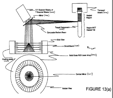
connection therewith. For example, RED based laser diodes may be
implemented in a variety of manners, an example of which will be described in
connection with Figure 13. In addition, various semiconductor lasers and other
laser diodes may be employed with suitable modifications. Of course, other
CA 02652585 2008-11-17
WO 2007/149221 PCT/US2007/013306
-28-
enabling technologies may be developed for efficiently producing limited
bandwidth irradiation in advantageous wavelengths.
In order to practice the invention for a particular application, it will
usually require deploying multiple devices to produce enough radiant heat
energy output in order to have adequate amplitude of irradiation. Again, in
one
form, these devices will be RED based laser diodes (also referred to as L-
REDs). In most heat applications of the invention, such devices will typically
be deployed in some sort of high density x by y array or in multiple x by y
arrays, some of which may take the form of a customized arrangement of
individual RED devices (again, in one form, L-REDs). The arrays can range
from single devices to more typically hundreds, thousands, or unlimited
number arrays of devices depending on the types and sizes of devices used,
the output required, and the wavelengths needed for a particular
implementation of the invention. The RED devices will usually be mounted on
circuit boards which have at least a heat dissipation capability, if not
special
heat removal accommodations. Often the RED devices will be mounted on
such circuit boards in a very high density/close proximity deployment. It is
possible to take advantage of recent innovations in die mounting and circuit
board construction to maximize density where desirable for high-powered
applications. For example, such techniques as used with flip chips are
advantageous for such purposes. Although the efficiency of the RED devices
is good for this unique class of diode device, the majority of the electrical
energy input is converted directly into localized heat. This waste heat must
be
conducted away from the semi-conductor junction to prevent overheating and
burning out the individual devices. For the highest density arrays, they may
likely use flip-chip and chip-on-board packaging technology with active and/or
passive cooling. Multiple circuit boards will often be used for practicality
and
positioning flexibility. The x by y arrays may also comprise a mix of RED
devices which represent at least two different selected wavetengths of
infrared
radiation in a range from, for example, 1 micrometer to 5 micrometers.
For most applications, the RED devices will be deployed
advantageously in variously sized arrays, some of which may be three
dimensional or non-planar in nature for better irradiation of certain types of
targets. This is true for at least the following reasons:
CA 02652585 2008-11-17
WO 2007/149221 PCT/US2007/013306
-29-
1. To provide sufficient output power by combining the output of the
multiple devices.
2. To provide for enough `spread' of output over a larger surface than a
single device could properly irradiate.
3. To provide the functionality that the programmability of an array of RED
devices can bring to an application.
4. To allow mixing into the array devices that are tuned to different
specified wavelengths for many functional reasons described in this
document.
5. To facilitate matching the `geometry' of the output to the particular
application requirement.
6. To facilitate 'matching the devices mounting location, radiating angles
and economics to the application requirements.
7. To facilitate the synchronization of the output to a moving target or for
other 'output motion'.
8. To accommodate driving groups of devices with common control
circuitry.
9. To accommodate multi-stage heating techniques.
Because of the typical end uses of diodes, they have been
manufactured in a manner that minimizes cost by reducing the size of the
junction. It therefore requires less semiconductor wafer area which is
directly
correlated to cost. The end use of RED devices will often require substantial
radiated energy output in the form of more photons. It has been theorized that
REDs could be manufactured with creative ways of forming a large photon
producing footprint junction area. By so doing, it would be possible to
produce
RED devices capable of sustaining dramatically higher mid-infrared, radiant
output. If such devices are available, then the absolute number of RED
devices needed to practice this invention could be reduced. It would .not
necessarily be desirable or practical, however, given the high power outputs
associated with the many applications of this invention, that the number of
devices would be reduced to a single device. The invention can be practiced
with a single device for lower powered applications, single wavelength
CA 02652585 2008-11-17
WO 2007/149221 PCT/US2007/013306
-30-
applications, or, if the RED devices can be manufactured with sufficient
output
capability.
Similarly, it is possible to manufacture the RED device arrays as
integrated circuits. In such an implementation the REDs would be arrayed
within the confines of a single piece of silicon, Gallium Arsenide, Indium
Phosphide, or other suitable substrate but with multiple junctions or an
enlarged bandgap areas that function as the photon production sites on the
chip. They could be similar to other integrated circuit packages which use
ball
grid arrays for electrical connectivity. Such device packages could then be
used as the array, facilitating the desired electrical connectivity for
connection
to and control by the control system. Again, an important design parameter is
the control of the junction or bandgap temperature which should not be
allowed to reach approximately 1000 to 1050 C, with current chemistries,
before damage begins to occur. For best efficiency, it is desirable to keep
the
bandgap area as cool as possible, like less than 30 degrees C, so that
maximum electrical current can be tolerated and converted to radiant photons.
Thus, the design for mounting each RED die to the circuit board, should
consider the importance of removing the heat from the device as efficiently as
possible. For example, heat can be removed by conduction through the stud
bumps that are also intended for electrical conduction to the anode and
cathode respectively of the device. The circuit board on which the devices are
mounted must be chosen for good heat conduction as well so that the heat
may be carried away from the devices which in many applications will employ
heat sinks or a cooling jacket as needed to keep the circuit board cool. It is
anticipated that future chemistry compounds may have increased heat
tolerance but heat must always be kept below the critical damage range of the
device employed. They could further be deployed either on circuit boards
individually or in multiples or they could be arrayed as a higher level array
of
devices as dictated by the application and the economics.
In designing the best configuration for deploying RED devices into
irradiation arrays, regardless of the form factor of the devices, the designer
must consider the whole range of variables. Some of the variables to be
considered in view of the targeted application include packaging, ease of
deployment, costs, electronic connectivity, control to programmability
CA 02652585 2008-11-17
WO 2007/149221 PCT/US2007/013306
-31-
considerations, cooling, environment of deployment, power routing, power
supply, string voltage, string geometry, irradiation requirements, safety and
many others that one skilled in the appropriate arts will understand.
All raw materials used to manufacture products have associated with
them particular absorption and transmission characteristics at various
wavelengths within the electromagnetic spectrum. Each material also has
characteristic infrared reflection and emission properties but we will not
spend
any time discussing these because the practicing of this invention is more
driven by the absorption/transmission properties. The percent of absorption at
any given wavelength can be measured and charted for any specific material.
It can then be shown graphically over a wide range of wavelengths as will be
explained and exampled in more detail later in this document. Because each
type of material has characteristic absorption or transmission properties at
different wavelengths, for best thermal process optimization it is very
valuable
to know these material properties. It should be recognized that if a certain
material is highly transmissive in a certain range of wavelengths then it
would
be very inefficient to try to heat that material in that wavelength range.
Conversely, if the material is too absorptive at a certain wavelength, then
the
application of radiant heating will result in surface heating of the material.
For
materials that are inefficient heat conductors, this is not usually an optimum
way to heat evenly through the material.
The fact that various materials have specific absorption or transmission
characteristics at various wavelengths has been well known in the art for many
years. Because, however, high-powered infrared sources were not available
that could be specified at particular wavelengths, or combinations of
wavelengths, it has not historically been possible to fully optimize many of
the
existing heating or processing operations. Since it was not practical to
deliver
specific wavelengths of infrared radiation to a product, many manufacturers
are not aware of the wavelengths at which their particular product is most
desirously heated or processed.
This is illustrated with an example in the plastics industry. Referring to
Figures 9 and 10, by examining the transmission curve of Polyethylene
terephthalate (PET resin material, as it is known in the industry), out of
which
plastic beverage containers are stretch blow molded, it can be observed that
CA 02652585 2008-11-17
WO 2007/149221 PCT/US2007/013306
-32-
the PET material is highly absorptive in the long wavelength region and is
highly transmissive in the visible and near-infrared wavelength regions. Its
transmission varies dramatically between 1 micrometers and 5 micrometers.
Its transmission not only varies dramatically in that range but it varies
frequently and abruptly and often very substantially sometimes within 0.1
micrometers.
For example, at 2.9 micrometers PET has a very strong absorption.
This means that if infrared radiation was introduced to PET at 2.9
micrometers,
it would nearly all be absorbed right at the surface or outer skin of the
material.
If it were desirable to heat only the outer surface of the material, then this
wavelength could be used. Since PET is a very poor conductor of heat (has a
low coefficient of thermal conductivity) and since it is more desirable in
stretch
blow molding operations to heat the PET material deeply from within and
evenly all the way through its volume, this is, in practice, a bad wavelength
at
which to heat PET properly.
Looking at another condition, at 1.0 micrometer (1000 nanometers) PET
material is highly transmissive. This means that a high percentage of the
radiation at this wavelength that impacts the surface of the PET, will be
transmitted through the PET and will exit without imparting any preferential
heating, hence be largely wasted. It is important to note that the
transmission
of electromagnetic energy decreases exponentially as a function of thickness
for all dielectric materials, so the material thickness has a substantial
impact
on the choice for the optimal wavelength for a given material.
It should be understood that while PET thermoplastic material has been
used here as an example, the principles hold true for a very wide range of
different types of materials used in different industries and for different
types of
processes. For example, PEN or PLA are materials to which these principles
may apply. As a very different example, a glue or adhesive lamination system
is illustrative. In this example, suppose that the parent material that is to
be
glued is very transmissive at a chosen infrared wavelength. The heat-cured
glue that is to be employed might be very absorptive at that same wavelength.
By irradiating the glue/laminate sandwich at this specific advantageous
wavelength, the process is further optimized because the glue, and not the
adjacent parent material, is heated. By selectively choosing these wavelength
CA 02652585 2008-11-17
WO 2007/149221 PCT/US2007/013306
-33-
interplays, optimum points are found within various widely diverse kinds of
processing or heating applications within industry.
Historically, the ability to produce relatively high infrared radiation
densities at specific wavelengths has simply not been available to industry.
Therefore, since this type of heating or processing optimization has not been
available, it has not been contemplated by most manufacturers. It is
anticipated that the availability of such wavelength specific infrared radiant
power will open entirely new methodologies and processes. The subject
invention will make such new processes practical and will provide an
implementation technology that has far reaching flexibility for a wide range
of
applications. While it is anticipated that the first utilizations of the
subject
invention will be in industry, it is also recognized that there will be many
applications in commercial, medical, consumer, and other areas as well.
It is anticipated that the invention will be very useful as an alternative to
broadband quartz infrared heating bulbs, or other conventional heating
devices, that are currently in wide usage. Such quartz bulbs are used for a
range of things including heating sheets of plastic material in preparation
for
thermo-forming operations. Not only can the subject invention be utilized as
an alternative to the existing functionality of quartz infrared lamps or other
conventional heating devices, but it can be envisaged to add substantial
additional functionality.
The present invention, by contrast, can either generate radiant energy
in a continuously energized or alternately a pulsed mode. Because the basic
RED devices of the subject invention have an extremely fast response time
which measures in microseconds, it can be more energy efficient to turn the
energy on when it is needed or when a target component is within the targeted
area and then turn it off when the component is no longer in the targeted
area.
The added functionality of being able to pulse energize the infrared
source can lead to a considerable improvement in overall energy efficiency of
many radiant heating applications. For example, by suitably modulating the
energized time of either individual or arrays of the infrared radiation
emitting
devices (REDs), it is possible to track individual targets as they move past
the
large infrared array source. !n other words, the infrared emitting devices
that
are nearest the target device would be the ones that would be energized. As
CA 02652585 2008-11-17
WO 2007/149221 PCT/US2007/013306
-34-
the target component or region moves onward, the "energizing wave" could be
passed down the array.
In the case of heating material which will be thermoformed, it could be
desirable to apply more heat input into areas which will get more severely
formed as compared to areas which will be more modestly formed or not
formed at all. It is possible, by correctly designing the configuration of
infrared
emitter arrays, to not only not have all the devices energized simultaneously
but it is possible to energize them very strategically to correspond to the
shape
of the area to be heated. For continuously moving production lines, for
example, it might be most desirable to program a specially shaped area of
desired heat profile that can be programmably moved in synchronous motion
with the target region to be heated. Consider a picture frame shaped area
requiring heating as shown in Figure 18. In this case, it would be possible to
have a similar picture frame shaped array of devices (402) at desired radiant
intensity that would programmably move down the array, synchronized with
the movement of the target thermoforming sheet (401). By using an encoder
to track the movement of a product such as the (401) thermoforming sheet,
well known electronics synchronization techniques can be used to turn on the
right devices at the desired intensity according to a programmable controller
or
computer's instructions. The devices within the arrays could be turned on by
the control system for their desired output intensity in either a"continuous'
mode or a "pulsed" mode. Either mode could modulate the intensity as a
function of time to the most desirable output condition. This control can be
of
groups of devices or down to individual RED devices. For a particular
application, there may not be a need, to have granular control down to the
individual RED devices. In these instances the RED devices can be wired in
strings of most desired geometry. These strings or groups of strings may then
be programmably controlled as the application requirements dictate.
Practicality will sometimes dictate that the RED devices are driven in groups
or
strings to facilitate voltages that are most convenient and to reduce the cost
of
individual device control.
The strings or arrays of REDs may be controlled by simply supplying
current in an open loop configuration or more sophisticated control may be
employed: The fact intensive evaluation of any specific application will
dictate
CA 02652585 2008-11-17
WO 2007/149221 PCT/US2007/013306
-35-
the amount and level of infrared radiant control that is appropriate. To the
extent that complex or precise control is dictated, the control circuitry
could
continuously monitor and modulate the input current, voltage, or the specific
output. The monitoring for most desirable radiant output or result could be
implemented by directly measuring the output of the infrared array or,
alternatively, some parameter associated with the target object of the
infrared
radiation. This could be performed by a continuum of different technologies
from incorporating simple thermocouples or pyrometers up to much more
sophisticated technologies that could take the form of, for example, infrared
cameras. One skilled in the art will be able to recommend a particular closed
loop monitoring technique that is economically sensible and justifiable for a
particular application of the invention.
Both direct and indirect methods of monitoring can be incorporated. For
example, if a particular material is being heated for the purpose of reaching
a
formable temperature range, it may be desirable to measure the force needed
to form the material and use that data as at least a portion of the feedback
for
modulation of the infrared radiation arrays. Many other direct or indirect
feedback means are possible to facilitate optimization and control of the
output
of the subject invention.
It should be clearly understood that the shapes, intensities, and
energizing time of the present invention radiant heat source, as described
herein, is highly programmable and lends itself to a very high level of
programmable customization. Often in industry, custom shapes or
configurations of heat sources are designed and built for a specific component
to direct the heating to the correct locations on the component. With the
flexible programmability of the subject invention it is possible for a single
programmable heating panel to serve as a flexible replacement to an almost
infinite number of custom-built panels. Industry is replete with a wide
variety of
infrared ovens and processing systems. Such ovens are used for curing
paints, coatings, slurries of various sorts and types, and many other
purposes.
They also can be used in a wide variety of different lamination lines for heat
fusing materials together or for curing glues, adhesives, surface treatments,
'
coatings, or various layers that might be added to the lamination 'sandwich'.
CA 02652585 2008-11-17
WO 2007/149221 PCT/US2007/013306
-36-
Other ovens may be used for a wide variety of drying applications. For
example, in the two-piece beverage can industry it is common to spray a
coating into the interior of the beverage can and then transport them
continuously by conveyor "in mass" through a long curing oven. The uncured
interior coating has the appearance of white paint upon application but after
curing becomes nearly clear. In these various drying and curing applications
with the current invention, it would be possible to choose a wavelength or
combination of wavelengths that are the most readily and appropriately
absorbed by the material that needs to be dried, treated, or cured. In some
applications the wavelengths that are not present may be more important to an
improved process than the ones that are present. The undesirable
wavelengths may adversely affect the materials by drying, heating, changing
grain structure or many other deleterious results which in a more optimum
process could be avoided with the subject invention.
Often it is desirable to raise the temperature of a target material to be
cured or dried without substantially affecting the substrate or parent
material.
It may well be that the parent material can be damaged by such processing. It
is more desirable to not induce heat into it while still inducing heat into
the
target material. The subject invention facilitates this type of selective
heating.
To review another application area for the invention, the medical
industry has been experimenting with a wide range of visible light and near-
infrared radiant treatments. It has been theorized that certain wavelengths of
electromagnetic energy stimulate and promote healing. It has also been
postulated that irradiation with certain wavelengths can stimulate the
production of enzymes, hormones, antibodies, and other chemicals within the
body as well as to stimulate activity in sluggish organs. It is beyond the
scope
of this patent to examine any of the specific details or treatment
methodologies
or the merit of such postulations. The subject invention however, can provide
a
solid state, wavelength selectable, and programmable mid-infrared radiation
source that can facilitate a wide range of such medical treatment modalities.
It is historically true however that the medical industry has not had a
practical methodology for producing high-powered, wavelength specific
irradiation in the mid-IR wavelength bands. The present invention would allow
for such narrow band wavelength specific infrared irradiation and it could do
so
CA 02652585 2008-11-17
WO 2007/149221 PCT/US2007/013306
-37-
in a slim, light weight, safe and convenient form factor that would be easily
used for medical applications.
For medical treatment there are some very important advantages to
being able to select the specific wavelength or combination of wavelengths
that are used for irradiation. Just as in industrial manufacturing materials,
organic materials also have characteristic transmission/absorption spectral-
curves. Animal, plant, or human tissue exhibits specific
absorption/transmissive windows which can be exploited to great advantage.
A very high percentage of the human body is composed elementally of
water, therefore it is likely that the transmission/absorption curves for
water are
a good starting point for a rough approximation for much human tissue.
Through extensive research it is possible to develop precise curves for all
types of tissue in humans, animals, and plants. It is also possible to develop
the relationship between various kinds of healing or stimulation that might be
sought from organs or tissue and relate that to the transmission/absorption
curves. By carefully selecting the wavelength or combination of wavelengths,
it would be possible to develop treatment regimens which could have a
positive effect with a wide range of maladies and ailments.
Some tissues or organs that it would be desirable to treat are very near
the surface while others lie deep within the body. Due to the absorption
characteristics of human tissue, it might not be possible to reach such deep
areas with non-invasive techniques. It may be necessary to use some form of
invasive technique in order to get the irradiation sources near the target
tissue.
It is possible to design the irradiation arrays of the present invention so
that
they are of the appropriate size and/or shape to be used in a wide range of
invasive or non-invasive treatments. While the treatment techniques,
modalities and configurations are beyond the scope of this discussion; the
invention is the first of its kind available to make solid state, wavelength
selective irradiation available in the middle-infrared wavelength bands. It
can
be configured for a wide range of modalities and treatment types. Due to its
highly flexible form factor and programmable nature it is capable of being
configured for a particular body size and weight to produce the appropriate
angles, intensities, and wavelengths for custom treatment.
CA 02652585 2008-11-17
WO 2007/149221 PCT/US2007/013306
-38-
Infrared radiation is being utilized for an increasing number of medical
applications from hemorrhoid treatments to dermatology. One example of
infrared treatment that is currently performed with broadband infrared sources
is called infrared coagulation treatment. Additionally, diabetic peripheral
neuropathy is sometimes treated with infrared lamp treatments. Tennis elbow
and other similar ailments are often currently treated with broadband infrared
lamps as well. The incorporation of the present invention's ability to
generate
specific wavelengths of radiation as well as its ability to generate pulsed
irradiation may provide substantial improvement in these treatments. It also
may provide for better patient toleration and comfort. The invention also
facilitates manufacturing a medical device that could be powered with
inherently safe voltages.
The pulsing of the irradiation energy may prove to be a key aspect
associated with many medical treatment applications. Continuous irradiation
may cause tissue overheating while a pulsed irradiation may prove to provide
enough stimulation without the deleterious effect of overheating, discomfort,
or
tissue damage. The very fact that the devices/arrays can be pulsed at
extremely high rates with turn-on times measured in microseconds or faster
provides another useful property. It is anticipated that very high intensity
pulses of radiation may be tolerated without damage to the arrays if they are
activated for very short duty cycles, since the semi-conductor junction
overheat
would not have time to occur with such short pulse times. This would allow
greater summed instantaneous intensity which could facilitate penetration
through more tissue.
The frequency at which the pulsing occurs may also prove to be
important. It is known within the literature that certain frequencies of
irradiation
to humans can have healing or, alternatively, deleterious effects. For
example,
certain amplitude modulation frequencies or combinations of frequencies of
visible light can cause humans to become nauseous and yet other amplitude
modulation frequencies or combinations of frequencies can cause epileptic
seizures. As further medical research is done it may indeed determine that the
pulsing frequency, waveform shape, or combination of frequencies along with
the selected wavelength or combination of wavelengths have a very
substantial effect on the success of various radiation treatments. It is very
CA 02652585 2008-11-17
WO 2007/149221 PCT/US2007/013306
-39-
likely that many of the treatment modalities which will utilize this invention
are
not yet understood nor realized since the subject invention has not been
available to researchers or practitioners.
Another application for the subject invention is in the preparation,
processing, or staging of food. Certainly a very wide range of different types
of
ovens and heating systems have been used in the preparation of food
throughout human history. Since most of them are well known, it is beyond the
scope of this patent application to describe the full range of such ovens and
heating systems. With the notable exception of microwave cooking which
utilizes non-infrared/non-thermal source cooking technology, virtually all
other
cooking technologies utilize broadband heating sources of various types. The
infrared heating sources and elements that are used in such ovens are broad-
band sources. They do not have the ability to produce specific wavelengths of
infrared energy that might be most advantageous to the particular cooking
situation or the product being cooked-.
As was discussed earlier with other materials, plant and animal
products have specific absorption spectral curves. These specific absorption
curves relate how absorptive or transmissive a particular food product is at
specific wavelengths. By selecting a particular wavelength or a few carefully
selected wavelengths at which to irradiate the subject food it is possible to
modify or optimize the desired cooking characteristics. The most efficient use
of radiated energy can reduce the cost of heating or cooking.
For example, if it is most desirous to heat or brown the outer surface of
a particular food product, the subject invention would allow for the selection
of
a wavelength at which that particular food product is highly absorptive. The
result would be that when irradiated at the chosen wavelength the infrared
energy would all be absorbed very close to the surface, thus causing the
desired heating and/or browning action to take place right at the surface.
Conversely, if it is desired not to overheat the surface but rather to cook
the.
food from very deeply within it, then it is possible to choose a wavelength or
combination of selected wavelengths at which the particular food is much more
transmissive so that the desired cooking result can be achieved. Thus the
radiant energy will be absorbed progressively as it penetrates to the desired
depth.
CA 02652585 2008-11-17
WO 2007/149221 PCT/US2007/013306
-40-
It is important to note that for electromagnetic'waves traveling through a
non-metallic material, the intensity of this wave i(t) decreases as a function
of
travel distance t as described by the following equation:
l(t) =lo(e" `c)
In this equation, lo is the initial intensity of the beam and a is the
specific
absorption coefficient for the material. As time t increases, the intensity of
the
beam undergoes exponential decay which is caused by radiant energy within
the original beam being absorbed by the host material. For this reason, the
use of infrared radiation heating to achieve optimum cooking results entails a
complex interaction between the thickness of the food items, the applied
infrared radiant intensity, the irradiation wavelength, and the material
absorption coefficient(s).
By mixing RED elements that irradiate at different wavelengths, it is
possible to further optimize a cooking result. Within such a multi-wavelength
array, one element type would be chosen at a wavelength wherein the
absorption of radiant energy is low, thus allowing deep-heat penetration to
occur. A second element type would be chosen wherein the absorption of
radiant energy is high thus facilitating surface heating to occur. Completing
the array, a third RED element type could be conceived to be chosen at a
wavelength intermediate to these two extremes in absorption. By controlling
the relative radiant output level of the 3 types of RED emitters contained in
such an array, it would be possible to optimize the important properties of
prepared food items.
By connecting color, temperature, and potentially visual sensors to the
control system it is possible to close the loop and further optimize the
desired
cooking results. Under such circumstances, it may be possible to check the
exact parameter which might be in question and allow the control system to
respond by sending irradiation at the appropriate wavelength, intensity, and
direction that would be most desirable. By utilizing and integrating a vision
sensor, it would be possible to actually view the locations and sizes of the
food
products that are to be cooked and then optimize the ovens' output accordingly
as has been described above. When used in combination with a moisture
sensor, it would be possible to respond with the combination that would
CA 02652585 2008-11-17
WO 2007/149221 PCT/US2007/013306
-41-
maintain the desired moisture content. It is, therefore, possible to
understand
how the subject invention, in combination with the appropriate sensors, and
controller "intelligence" can truly facilitate the smart oven of the future.
It is, of
course, possible to combine the present invention with conventional cooking
technologies, including convection ovens and microwave oven capability to get
the best blend of each of these technology offerings. The smart control
system could be designed to best optimize both the present invention
technology in combination with the conventional cooking technologies.
It is also possible, by selecting wavelengths that would be absorbed by
one food and not as highly absorbed by a second food, to be very selective as
to the amount of heating that takes place in a mixed plate of food. Thus it
can
be understood that by changing the combinations and permutations and
intensities of various wavelengths that are selectable one could achieve a
wide
range of specifically engineered cooking results.
With any of the applications of the subject invention, it is possible to use
various lensing or beam guiding devices to achieve the desired directionality
of
the irradiation energy. The chosen beam guiding devices must be chosen
appropriately to function at the wavelength of radiation that is being guided
or
directed. By utilizing well understood techniques for diffraction, refraction,
and
reflection, it is possible to direct energy from different portions of an
array of
RED devices in desired directions. By programmably controlling the particular
devices that are turned on, and by modulating their intensities, it is
possible to
achieve a wide range of irradiation selectivity. By choosing steady state or
pulsing mode and by further programming which devices are pulsed at what
time, it is possible to raise the functionality even further.
Though this disclosure discusses the application of radiant energy
primarily within the 1.0 to 3.5 micrometers range, it should be obvious to
anyone skilled in the art that similar material heating effects can be
achieved at
other operational wavelengths, including longer wavelengths in the infrared or
shorter wavelengths down through the visible region. The spirit of the
disclosed invention includes the application of direct electron-to-photon
solid-
state emitters for the purposes of radiant heating wherein the emitters are
conceivably operational from the visible through the far infrared. It may be
desirable to, for certain types of applications, to combine other wavelength
CA 02652585 2008-11-17
WO 2007/149221 PCT/US2007/013306
-42-
selectable devices into the invention which irradiate at other wavelengths
outside the mid-infrared range.
Figure 8 gives a graphical indication of a single RED component 10.
The RED 10 comprises a stack 20. The stack 20 may take a variety of
configurations, such as the stacks of semiconductor layers and the like
illustrated in connection with Figures 1-7. In at least one form, the contact
40
(corresponding, for example, to contacts 1105, 1205 and 1305) of the RED 10
is made to the stack 20 through wire 80. When a current 60 is made to flow
through the bonding wire 80 and the stack 20, photons 70 are emitted that
possess a characteristic energy or wavelength consistent with the
configuration of the stack 20.
Because many of the semi-conductor lessons learned in manufacturing
LEDs may apply to REDs, it is useful to mention a parallel that may help the
evolution of the new RED devices. Drastic improvements in the energy
conversion efficiency (optical energy out/electrical energy in) of LEDs have
occurred over the years dating to their introduction into the general
marketplace. Energy conversion efficiencies above 10% have been achieved
in commercially available LEDs that operate in the visible light and near IR
portion of the spectrum. This invention contemplates the use of the new REDs
operating somewhere within the 1 micrometer to 3.5 micrometer range as the
primary infrared heating elements within various heating systems. This
application describes a specific implementation in blow molding systems.
Figures 9 and 10 show the relative percentage of IR energy transmitted
within a 10 mil thick section of PET as a function of wavelength. Within the
quartz transmission range (up to 3.5 micrometer), the presence of strong
absorption bands (wavelength bands of little or no transmission) are evident
at
several wavelengths including 2.3 micrometer, 2.8 micrometer, and 3.4
micrometer. The basic concept associated with the subject invention is the use
of RED elements designed and chosen to operate. at a selected wavelength(s)
within the 1 micrometer to 3.5 micrometer range as the fundamental heating
elements within the thermal conditioning section of blow molding machines.
Figures 11 a, 11 b, and 11 c show an example ensemble of individual
RED emitters 10 packaged together into a suitable RED heater element 100.
In this embodiment of the invention, the REDs 10 are physically mounted so
CA 02652585 2008-11-17
WO 2007/149221 PCT/US2007/013306
-43-
that N-doped regions are directly attached to a cathode bus 120. The cathode
bus 120 is ideally fabricated out of a material such as copper, or gold, which
is
both a good conductor of electricity as well as heat. The corresponding
regions
of the REDs 10 are connected via bond wires 80 to the anode bus 110. Ideally,
the anode bus would have the same thermal and electrical properties as the
cathode bus. input voltage is externally generated across the 2 bus bars
causing a current (I) to flow within the REDs 10 resulting in the emission of
IR
photons or radiant energy, such as that shown at 170. A reflector 130 is used
in the preferred embodiment to direct the radiant energy into a preferred
direction away from the RED heater element 100. The small physical extent of
the REDs 10 make it possible to more easily direct the radiant energy 170 that
is emitted into a preferred direction. This statement being comparatively
applied to the case of a much larger coiled filament; such a relationship*
between the physical size of an emitter and the ability to direct the
resultant
radiant flux using traditionai- lensing means being well known in the art.
A heat sink 140 is used to conduct waste heat generated in the process
of creating IR radiant energy 170 away from the RED heater element 100. The
heat sink 140 could be implemented using various means known within
industry. These means include passive heat sinking, active heat sinking using
convection air cooling, and active heat sinking using water or liquid cooling.
The liquid cooling through, for example, a liquid jacket has the advantage of
being able to conduct away the substantial amount of heat that.is generated
from the quantity of electrical energy that was not converted to radiant
photons. Through the liquid media, this heat can be conducted to an outdoor
location or to another area where heat is needed. If the heat is conducted out
of the factory or to another location then air conditioning/cooling energy
could
be substantially reduced.
Additionally, a bulb 150 is optimally used in this embodiment of the
invention. The primary function of the bulb 150 as applied here is to protect
the
REDs 10 and bonding wires 80 from being damaged. The bulb 150 is
preferably constructed out of quartz due to its transmission range that
extends
from the visible through 3.5 micrometer. However, other optical materials
including glass having a transmission range extending beyond the wavelength
of operation of the REDs 10 could also be used.
CA 02652585 2008-11-17
WO 2007/149221 PCT/US2007/013306
-44-
One deployment of the RED heater element 100, within a blow molder,
is depicted in Figures 12a and 12b. In this system, preforms 240 enter into a
thermal monitoring and conditioning systeri~ 210 via a transfer system 220.
The preforms 240 could come into the thermal monitoring and control system
210 at room temperature, having been previously injection molded at some
earlier time. Or, alternatively, the preforms 240 could come directly from an
injection molding process as is done in single-stage injection molding/blow
molding systems. Alternatively, the preforms could be made by one of several
other processes. Whatever the form and timing of preform manufacturing,
entering in this fashion, the preforms 240 would have varying amounts of
latent
heat contained within them.
Once presented by the transfer system 220, the preforms 240 are
transported through the thermal monitoring and control system 210 via a
conveyor 250, such conveyors being well known in industry. As the preforms
240 travel through the thermal monitoring and control system 210, they are
subjected to radiant IR energy 170 emitted by a series of RED heater elements
100. These RED heater elements may advantageously take the form of laser-
.based RED elements (L-REDs), which will be described in further detail below.
The IR energy 170 emitted by these RED heater elements 100 is directly
absorbed by the preforms 240 in preparation of entering the blowing system
230. It should be appreciated that the energy may be continuous or pulsed, as
a function of the supply or drive current and/or other design objectives. The
control system, such control system 280, in one form, controls this
functionality. As an option, the control system is operative to pulse the
system
at electrical current levels that are substantially greater than recommended
steady state current levels to achieve higher momentary emitted intensity in
pulsed operation and respond to an input signal from an associated sensor
capability to determine a timing of the pulsed operation
In the preferred embodiment of a blow molder operating using the
method and means described by this invention, a convection cooling system
260 is also preferably deployed. This system removes waste heat from the air
and mechanics that are in proximity to the preforms 240 under process. A
conduction cooling device may also be employed to do so. Heating of
preforms by convection and/or conduction is known in the art to be deleterious
CA 02652585 2008-11-17
WO 2007/149221 PCT/US2007/013306
-45-
to the overall thermal conditioning process. This is because PET is a very
poor thermal conductor and heating the outer periphery of the preform results
in uneven through heating, with too cool a center and a too warm outer skin.
Also contained within the preferred system embodiment are
temperature sensors 270 (which may take the form of an intelligent sensor or
camera that is capable of monitoring a target in at least one aspect beyond
that which a single point temperature measurement sensor is capable) and a
temperature control system 280. These aspects of the preferred blow molder
design are particularly applicable to the attributes of a one-stage blow
molding
system. In a one-stage blow molding system, the preforms 240 enter into the
thermal monitoring and'conditioning system 210 containing latent heat energy
obtained during the injection molding stage. By monitoring the temperature
and thus the heat content of the incoming preforms 240 (or specific
subsections of such performs), it is possible for a temperature monitoring and
control system 280 to generate preform-specific (or subsection specific)
heating requirements and then communicate these requirements in the form of
drive signals to the individual RED heater elements 100. The solid-state
nature
and associated fast response times of RED emitters 10 make them particularly
suited to allow the electrical supply current or on-time to be modulated as a
function of time or preform movement. Also, subsections of the RED array
may be controlled, as will be appreciated.
The temperature control system 280 used to enact such output control
could be implemented as an industrial PC as custom embedded logic or as or
an industrial programmable logic controller (PLC), the nature and operation
all
three are well known within industry. The control system, such as that shown
as 280, may be configured a variety of ways to meet the objectives herein.
However, as some examples, the system may control on/off status, electrical
current flow and locations of activated devices for each wavelength in an RED
array.
In still another technique implemented according to the present
invention, a method for heating the container using laser radiation is
provided.
The laser light illuminates the container, normally in its "preform" stage,
so,as to
soften it.through the absorption of light. The container is subsequently blow
formed. The method of delivering the energy, and the choice of wavelength(s)'
CA 02652585 2008-11-17
WO 2007/149221 PCT/US2007/013306
-46-
can be varied, in accordance with the needs of the application. In one form,
the
selected narrow wavelength range may be specifically tuned to the heating
requirements of the material from which the particular target component is-
manufactured. Although it is possible to manufacture the diode devices to near-
monochromatic wavelength specificity, it is not usually needed to be that
narrow.
Often, if the wavelength is centered in the absorption band correctly, plus or
minus 20 or even 50 nanometers may be just fine. Other applications, because
of
the narrowness or proximity of the absorption bands, may need to have a very
narrow wavelength tolerance. The selected wavelengths chosen for use may be
anywhere in the range from 1.0 to 5.0 microns, or may, more practically, be
selected from the narrower range of 1.5 to 3.5 microns. The absorption rate
characteristics of the material at the different wavelengths is a factor. If
more than
one absorber is involved, a "door and window" evaluation may be appropriate
if,
for example, one material is to be heated but not the other. One will need to
determine if wavelengths can be chosen such that one material is a poor
absorber while, at that same wavelength, the other is a strong absorber. These
interplays are a valuable aspect of the present invention. By paying close
attention to the absorptions and/or the interplays, system optimization can be
achieved. The absorption band for a particular material may be selected based
on, or to optimize, desired depth of heating, location of heating, speed of
heating
or thickness to be heated. In addition, the laser diodes (or other devices)
contemplated herein may be used to pump other oscillating elements to achieve
desired wavelengths.
The proposed method quickly solves most of the aforementioned issues,
and renders irrelevant the remainder. The principal requirement for any
radiative heat transfer method is matching the spectral absorption of the
material to the spectral output of the radiating source. Standard lasers have
many wavelengths from which to choose for satisfying this requirement. Wall
plug
efficiency for most lasers is between 10 and 20%, which, when matched
properly to the absorption of the target, will result in 8-15% heat transfer
efficiency, compared to only several % for the existing method. The spatial
coherence of laser light allows it to be placed exactly where it is needed.
This
contrasts favorably to the standard practice, where the light is emitted in
all
directions from the bulb filament, and must be collected and pointed in the
CA 02652585 2008-11-17
WO 2007/149221 PCT/US2007/013306
-47-
correct direction. The physics of extended sources renders this very
inefficient.
The coherence of the laser light is not relevant to this method, but the
brightness, or the "directedness" is critical. Lasers are inherently bright,
and
laser light of the appropriate wavelengths propagates through free space with
little loss, hence extraneous heating is no longer an issue. Lasers are
typically
water cooled, and excess heat goes into the water jacket, not ambient, making
heat management much more straightforward. Many lasers are also instantly
adjustable, over a wide range of intensities, and in some applications, their
spatial intensity is rapidly adjustable as well.
There are two main approaches to the deposition of laser energy on a
target: a stationary shaped beam, and an adjustable-scanning beam. They will
be described separately.
In a first approach using a stationary beam, the laser light is shaped
refractively or diffractively, to the desired spatial and intensity profile,
before it
strikes the plastic target component or a container preform. For a typical
preform, which is nominally cylindrical, a combination of lenses is used to
expand and collimate the beam, then a simple cylinder lens is adequate to
produce a rectangular profile. The nominal Gaussian intensity profile of the
typical TEMoo laser output can be modified as well with several methods,
.depending on desired final intensity profile. For uniform irradiance, a "top
hat", or
flat top profile is desirable, and can be produced by several well known
methods,
such as faceted beam integrators, holographic elements (HOE), and microlens
arrays. Non-uniform distributions are usually more appropriate, as different
-segments of the container typically require more heat. These can be best
accomplished with HOEs, although they can also be generated with beam
apodizers. However, apodizers work by selectively absorbing'portions of the
beam, and lead to increased inefficiency.
The ideal system would start with the choice of laser wavelength. This is
driven.by the container material and thickness. For a PET preform with 4 mm
walls, then a wavelength around 2um would provide for about 90% absorption
through the entire thickness of both walls of the preform. This is determined
by
using Beer's law and the coefficient of absorption for PET (alpha). There are'
several lasers to choose from that emit around 2 microns ; Raman shifted YAG,
Ho:YAG, and Tm:YAG. These are all YAG variant solid state lasers, and are
CA 02652585 2008-11-17
WO 2007/149221 PCT/US2007/013306
-48-
very reliable. Spatial and irradiance profiling of the beam is best
accomplished
by a combination of diffractive and refractive elements, For instance, the
beam
is expanded, collimated, and homogenized by a Galilean expander, followed by a
faceted beam integrator. The resultant square, uniform intensity beam strikes
an
HOE, which has been designed to change the input into a rectangular shape
with an intensity profile which is higher at the top and is reduced to about
1/2
max at the bottom. The exact shape is dependent on the container, but most
require more heating at the top. HOEs are very efficient devices, and are
relatively inexpensive to manufacture. However, some, materials may require
longer wavelength lasers, requiring exotic material for the HOEs.
The remainder of the system requires a means of triggering the laser to
expose the container preform at the time when it is in the center of the
irradiation pattern. It is not necessary, and may be advantageous, for the
spatial profile to be smaller than the container itself, and for the pulse
duration
to be long enough for the container preform to sweep through the profile.
Some means for providing multiple exposures is required as well, because
each container preform will need multiple exposures or a prescribed length of
exposure time. This can be accomplished by several means, the most direct of
which is to have a mirror arranged to follow a container for a specified
distance, thus allowing the intensity profile to be maintained on it for a
longer
time. Often, it will be desirable for the target to rotate as it is traversing
through the exposure area so that all sides may be exposed to the radiant
energy.
Another approach is through the use of a scanning beam. The primary
difference between the stationary and scanned beam approaches is in the
replacement of all of the beam shaping apparatus with two devices; an electro-
mechanical, servoed, or acousto-optical scanner, and: some means for variable
attenuation. The operative principle is to deposit energy from the raw laser
beam into the target component by rapidly scanning the beam across the
surface of it. If the scan rate of the laser is very fast relative to the
motion of the
targeted component and the desired rate of heating, then there is no
difference
between the two methods, from the target's perspective. All of the other
considerations apply, but avoiding the extra optics can be advantageous. The
scanned approach does not require HOEs to be designed and manufactured
CA 02652585 2008-11-17
WO 2007/149221 PCT/US2007/013306
-49-
beforehand. Spatial profiles are implemented by changing the scan limits, and
intensity changes can be implemented by either slowing the scanner down
where more heat is desired, or re-scanning some areas, or dithering die scan.
It is also possible to implement an active attenuator, either in the laser
itself, or
a lambda/2 plate, for polarization based attenuation. Any method which causes
the laser to put out less optical power for the same input power will
adversely
affect efficiency;. Changing the scan is preferable.
This approach has another benefit, in that following the target while it
proceeds through the tunnel is built into this approach, whereas some form of
it
must be adapted to the "stationary" beam approach to account for the targeted
component rapidly moving in and out of the-profile too quickly to absorb
enough
energy with just the one pass.
With reference to Figure 13, a system 2000 is illustrated. It should be
understood that the system couid be adopted to be a scanning system or a
stationary system. Selection of one of those systems is a function of whether
certain components (as will be described ) are rendered movable. In addition,
as
shown, the system uses laser diodes (e.g. L-REDs) and could be used as a
replacement for the heater elements 100 and otherwise integrated into the
system of Figures 12a and b. Minor modifications to the system, including the
thermal monitoring and control system 210 may be desired to accommodate the
replacement; however, any such changes will be apparent to those skilled in
the
art. For example, control of the system through use of the control subsystem
280 may be adapted to also include control of the scanner device (to be
described) of the system to achieve timing in the system so that the laser
diode
output energy is synchronized to the conveyance. Likewise, pulsing and
continuous mode operation would be controlled in the system by the control
subsystem 280 and other components of the system.
The system 2000 includes an implementation of an RED based laser
diode array to generate that appropriate energy wavelengths contemplated by
the subject embodiments. As shown, the system 2000 includes a solid state
RED based laser array 2002, a scanner means 2004 and a transport system
2006 for exemplary target components or preforms 2008 to deliver the
components to a thermal treatment region of the system. The array 2002
includes a circuit board supporting the RED based laser diode devices 2010
CA 02652585 2008-11-17
WO 2007/149221 PCT/US2007/013306
-50-
supported within a cooling jacket 2012. In one form, the array is operative to
emit one or more selected wavelengths of infrared radiant energy within the
wavelength range from 1.0 to 5.0 microns via direct electrical current-to-
photon
conversion process. The L-REDs are disposed in the array in an arrangement
which facilitates emitting a substantial portion of energy into the target
components. The array 2002 also uses a conical mirror 2014. The scanner
means may be an X-Y scanner or simply a Y scanner supporting a mirror 2016.
To render the system as scanning, at least one of the array 2002, scanner
means 2004, and/or the transport means 2006 is put in motion during the
generation of laser beams. Those of skill in the field will have an
understanding
of the various manners in which such motion can be generated. However, as but
one example, the scanner means 2004 may take the form of a galvanometer that
is capable of moving a mirror in the X and Y directions. This X and Y motion
would typically be programmably controlled to repeat the motion that is the
desired radiation pattern. This would allow for areas of the target components
to
be radiated by the laser beams.
As another exampfe, the system may be set-up to take advantage of the
fact that the target components may be in motion in one direction (e.g. the X
direction) as they are conveyed by the transport system 2006. In this case,
the
scanner means need only be operable to move the beams in, for example, the Y
direction to achieve irradiation of selected areas of the target components.
If the objective is to achieve a stationary beam, the components of the
system could be rendered stationary, and selected points on the target
components being transported by the transport means could be irradiated. In at
least one form, with reference back to Figure 12, each laser diode of an array
of
laser diodes could be focused on specific points, for example. It may be
desired
to use a beam expander lens in order to make sure that the array of projected
lasers have the desired coverage area and beam overlaps which would be
appropriate to the application. In this case one or both of the scanner means
or
the conical mirror, might not even be necessary.
It should be further appreciated that individual L-REDs may or may not
use any collimation or focusing techniques, depending on the specific
application. There may be applications where diverging energy of the diodes
may provide better coverage or beneficial overlap by way of the wider field of
CA 02652585 2008-11-17
WO 2007/149221 PCT/US2007/013306
-51-
view than a more conventional, collimated laser beam. If disposed in an array,
the output patterns of such devices may overlap to adequately and more
desirously cover the surface of a target. Also, combinations of L-REDs with
some having collimated or focused beams and other L-REDs having diverging
irradiation beams may be implemented. Nonetheless, as shown in Figures 13a
and 13b, in.operation, the system 2000 is able to generate laser beams from
the
array of diodes 2002. The array may take a variety of configurations to suit
the
application. For example, the array may contain devices generating a single
wavelength or multiple wavelengths. In one form, devices generating a first
wavelength of energy may be strategically mixed with devices generating a
second wavelength of energy to achieve a desired result. In one form, as
shown,
the x-by-y array of diodes is shaped into at least a portion of a cylindrical
configuration to facilitate the ultimate delivery of energy from the laser
source to
the target component. As shown, these beams are directed toward a non-
planar, e.g., a generally conical, mirror 2014 which reflects the rays toward
the
scanner device or means 2004. It should be appreciated that any suitable non-
planar mirror may be implemented, any such mirror being shaped to facilitate
improved delivery of thermal infrared radiant energy from the laser diodes
into
the target component, or portions of the target component. The scanner device
2004 then focuses the rays onto selected regions of the target component 2008,
e.g. a preform as shown. It should be understood that a variety of forms of a
scanner device 2004 may be implemented. For example, multiple scanners may
be implemented, the exact number of which depends on the speed of
processing, the number of target components, etc. In one form, as shown in
Figure 13b, multiple scariners 2004 are shown as being positioned to
adequately
inject heat into a plurality of target components in, for example, a blow
molding
environment. Of course, in the environment of a slower process, or an
environment of scanners having improved speed of operation, fewer scanners
may accomplish the application. In some applications, a single scanner may
suffice.
Referring back now to Figure 13(b), multiple scanner devices 2004 are
displayed in the system 2000. The optional conical mirrors 2002 are
representatively shown in association with each scanner device 2004. A
conveyance device, such as at 2006, and product carrier sites 2007 are also
CA 02652585 2008-11-17
WO 2007/149221 PCT/US2007/013306
-52-
shown. A tracking arc 2005 for laser 6 (one of the scanner devices 2004) and
example irradiation beams 2003 are also illustrated. An assignment chart is
displayed to illustrate the operation of the system. As shown, laser 1
irradiates
the first, seventh, thirteenth,...etc. target component as it passes by the
laser 1.
The other laser scanner devices irradiate respective components as shown in
the chart. A similar or programmed tracking arc to that of arc 2005 is
possessed
by each scanner device. In this manner, each component is irradiated for a
sufficient amount of time and can be irradiated specific to its needs. Of
course,
the number of scanners, the tracking arcs, and number of components treated by
each scanner device will vary as a function of the design and objectives of a
particular system.
Further, the scanner device 2004 may have a mirror 2016 associated
with the scanner device, the mirror 2016 being operative to direct the radiant
energy into the selected portions of the target components. The device may
also be capable of redirecting the radiant energy within a planar, two
dimensional scanning region, whereby a third dimension of motion is provided
by a conveyance means which moves the target through the irradiation region.
The device may also be capable of redirecting the radiant energy within a
three dimensional scanning region. In at least one form, the scanning device
is programmable so the at least one of the amount of time, quantity of
irradiation, or the placement of the irradiation can be controlled through
signals
determined by the control system. In one form, input to the control system is
supplied by temperature sensors or cameras (e.g. infrared cameras) which, in
conjunction with suitable routines, can determine the amount and timing of
irradiation required. This configuration provides suitable feedback for
closing
the loops on the system.
It should also be appreciated that, although an array of laser diodes or L-
REDs are described in connection with Figures 12a and b and 13a and b, an
appropriately powered single laser system may be used to generate the desired
irradiation. Such a system would require changes to the systems of Figures 12a
and b and 13a and b to accommodate the architecture of a single, more powerful
laser, however. Any such changes will be apparent to those of skill in the
art. It
should also be understood that various combinations of solid state lasers,
laser
diodes, L-REDs, and traditional laser systems (as well as REDs) may be
CA 02652585 2008-11-17
WO 2007/149221 PCT/US2007/013306
-53-
implemented to achieve the objectives of power and wavelength(s) of the
invention. In addition, other technologies may be combined with the various
combinations contemplated herein to enhance the implementation. For example,
fiber optic technology may be used to gather energy at the laser source and
deliver it to the contemplated target area. The use of fiber optic
configurations
may replace other types of optics that may be used to collimate or focus the
transmitted energy.
Figures 14-17 illustrate methods according to the present invention. It
should be appreciated that these methods may be implemented using suitable
software and hardware combinations and techniques. For example, the noted
hardware elements may be controlled by a software routines stored and
executed with the temperature control system 280.
Referring now to Figure 14, a preferred method 300 for the thermal
treatment of thermoplastic preforms is shown outlining the basic steps of
operation. Preforms 240 are transported via a conveyor 250 through a thermal
monitoring and control system 210 (Step 305). Of course, it should be
understood that, with all embodiments showing conveyance, a simple means
to locate the articles for exposure, with or without conveyance, may be
employed. The preforms 240 are irradiated using scanning thermal infrared
lasers (e.g.-an array 2002 of laser-based REDs or laser diodes) contained
within the thermal monitoring and control system 210 (Step 310). A convection
cooling system 260 is used to remove waste heat from the air and mechanical
components within the thermal monitoring and control system 210 (Step 315).
Another method 301 for the treatment of thermoplastic preforms is
outlined in Figure 15. In method 301, (Step 310), the process of irradiating
preforms 240 using scanning infrared lasers (e.g.laser-based REDs.or laser
diodes) is replaced with Step 320. During Step 320 of method 301, preforms
240 are irradiated synchronously to their motion through the thermal
monitoring and conditioning system 210. This synchronous, pulse irradiation
provides substantial additional energy efficiency because the L-RED devices
that are currently aimed at the perform are the only ones that are turned on
at
any given instant. In one form, the maximum output of the pulsed energy is
synchronously timed to the transport of individual targets.
CA 02652585 2008-11-17
WO 2007/149221 PCT/US2007/013306
-54-
Yet another method 302 for the treatment of thermoplastic preforms is
outlined in Figure 16. In this method 302, the temperature of incoming
preforms 240 is measured using temperature sensors 270. This is done to
gauge the latent heat energy of preforms 240 as they enter into the system
(Step 325) and therefore, how much heat (or exposure time) must be added to
bring it up to the desired temperature for proper blowing. The preforms 240
are then transported via a conveyor 250 through a thermal monitoring and
control system 210 (Step 305). A temperature control system 280 using the
temperature information supplied by the temperature sensors 270 to generate
a preferred control signal to be applied to the scanning infrared laser
subsystem (e.g. an array of laser-based REDs or laser diodes) (Step 330).
The preferred control signal is then communicated from the temperature
control system 280 to the scanning infrared laser subsystem (Step 335). The
preforms 240 are then irradiated using the lasers contained within the thermal
monitoring and control systems 210 (Step 310). A convection cooling system
260 is then used to remove waste heat from the air and mechanical
components within the thermal monitoring and control system 210 (Step 315).
Still another method 303 of the treatment of thermoplastic preforms is
outlined in Figure 17. In method 303, Step 310, the process of irradiating
preforms 240 using a scanning infrared laser subsystem (e.g. having an array
of laser-based REDs or laser diodes), is replaced with Step 320. During Step
320 of method 303, preforms 240 are pulse irradiated synchronously to their
motion through the thermal monitoring and conditioning system 210.
The above description merely provides a disclosure of particular
embodiments of the invention and is not intended for the purpose of limiting
the same hereto. As such, the invention is not limited to only the above-
described applications or embodiments. This disclosure addressed many
applications of the invention broadly and one application embodiment
specifically. It is recognized that one skilled in the art could conceive of
alternative applications and specific embodiments that fall within the scope
of
the invention.