Note: Descriptions are shown in the official language in which they were submitted.
CA 02652586 2014-04-24
DESCRIPTION
Wear Resistant Coating
Field of Invention
[00011 This invention relates to hard, wear resistant coatings vapour
deposited over a
metallic or non-metallic surface, in particular, the invention relates to a
coating to be
deposited on rotary tools having cutting edges utilized in industrial, medical
and dental
cutting, and form scraping, and is more particularly directed to improvements
in blades and
rotary cutting instruments.
Background of the Invention
[0002] Hard wearing surfaces are in common use in various industries, and
such hard
wearing surfaces are frequently obtained by coating the surface of a tool made
of steel or
similar metal, or other hard, enduring material, with a layer of hard wearing
ceramic
substance, such as carbides, nitrides and carbonitrides, or providing a hard
mierocrystalline
diamond coating. There are known methods for obtaining hard wearing coatings,
such as
for example, having a coating of diamond particles in combination with a
carbide or nitride
layer and then filling the gaps between the abrasive particles with a softer
intermetallic
compound. Another known method is vapour deposition of hard-wearing ceramic
materials from plasma or by utilizing molten ceramic substances. Hard wearing
surfaces
for use on medical, surgical and dental tools have additional requirements, as
such surgical
and dental tools need to be frequently sterilized, hence medical tools have to
be corrosion
resistant.
CA 02652586 2008-11-17
WO 2007/136777 PCT/US2007/011952
=
2
[0003] A device for yielding hard ceramic surfaces by cathodic arc plasma
deposition
is described in U.S. 4,851,095, issued to M.A. Scobey et al. on July 25, 1989.
The
apparatus of Scobey et al. utilizes a high intensity ion flux. Vapour
deposition of a hard
ceramic material, such as titanium or zirconium nitride, on a stainless steel
or titanium
surface by utilizing a molten evaporant and a hollow cathode, is described in
U.S. patent
5,152,774, issued to W.A. Schroeder on October 6, 1992. The vapour deposition
of
Schroeder is conducted at relatively low temperature, thus the substrate will
have lost little
of its initial high strength properties, however, the requirement of low
surface roughness of
the deposited layer is not addressed by U.S. 5,152,774. In U.S. 4,981,756,
issued to H.S.
Rhandhawa on January 1, 1991, a method is taught to coat surgical tools and
instruments
by cathodic arc plasma deposition. The ceramic coating obtained by this
technology is a
nitride, carbide or carbonitride of zirconium or hafnium, in a single layer of
3-10 m
thickness. U.S. 4,981,756 also refers to various publications describing known
equipment
for obtaining hard-wearing surfaces by cathodic arc plasma deposition. U.S.
patents
5,940,975 and 5,992,268 issued to T.G. Decker et al. on August 24, 1999 and
November
30, 1999, respectively, teach hard, amorphous diamond coatings obtained in a
single layer
on thin metallic blades or similar metallic strips utilizing filtered cathodic
arc plasma
generated by vaporizing graphite. It is noted that no interlayer is formed
between the blade
surface and the deposited amorphous diamond coating.
[0004] The grain size of deposits obtained in conventional cathodic plasma
arc
methods may range between 0.5 to 10gm. Any post-deposition heat treatment
which may
be required to maintain maximum hardness of the substrate's core metal, may
lead to
internal stresses in the coating due to differences in the grain size, and can
eventually lead
to abrasion, spalling, crack formation, grain separation, surface fractures,
uneven edges and
rough surfaces, and the like, which can drastically reduce the wear resistance
and durability
of surgical instruments and dental tools. None of the above discussed methods
are
concerned with even grain size and surface structure, and low micro-roughness
of the
vapour deposited hard, ceramic coatings, which have particular importance for
dental and
surgical tools, and in other applications where straight, sharp, even and nick-
free edges are
essential requirements.
CA 02652586 2008-11-17
WO 2007/136777 PCT/US2007/011952
3
[0005] Users desire cutting blades with sharp edges possessing long life
and corrosion
resistance. Typically, blades are initially sharpened to form a wedge shaped
cutting edge
and re-sharpened as needed, except in the case of razor blades which cannot be
re-
sharpened. Sharpness of a cutting blade is measured in terms of "ultimate tip
radius", ,
which is different depending on the application. For kitchen knives, rotary
cutters, and
similar cutting instruments, ultimate tip radius may be several thousand
Angstroms. In
agricultural implements incorporating rotary blades that cut through the soil,
axes, and in
chisels, the cutting edge radius may be expressed in microns or even in
millimeters rather
than Angstroms. Shaving razor blades ordinarily have ultimate tip radii of
about 1,500
Angstroms or less. This radius usually includes a layer of hard material
coating applied to
the wedge shaped base material of the razor blade. A self-sharpening blade
having a cutting
edge with different hardness and wear resistance on opposite sides of the
blades, provided
by applying different coating layers on opposite sides of the blade is
described in
U.S.6,105,261,issued to Ecer on August 22, 2000. This invention provides a
solution to the
problem of the cutting edge dulling by providing self-sharpening cutting edges
with
different hardness and wear resistance on opposite sides of the edge while
both sides have
micro-hardness and wear resistance significantly greater than the substrate
metal. Cutting
areas are kept sharp longer with this method especially in such adverse
environments as in
dental/surgical applications, use as saw blades and scrapers and in the
construction
industry. The disadvantage of this approach is that more intensive wear on one
side of the
edge leaves the hard layer unsupported which eventually results in a failure
of the more
brittle hard layer by fracturing. The soft side of the cutting edge has a
higher wear rate
which affects the support of the brittle thin film coating on the opposite
side.
[0006] Coatings such a TiN, Ti(CN), or (TiAl)N deposited onto the blade
edge region
of a steel knife blade blank by a cathodic arc process with simultaneous
heating and
rotation of the blade blank relative to the deposition sources are described
in US Patent
no.5,724,868, issued to Knudsen et al. The blade edge region may be sharpened
or
unsharpened prior to deposition of the coating material. If the blade edge
region is
unsharpened prior to deposition, it is thereafter sharpened, preferably on one
side only. An
improvement of this method was proposed in US Patent no. 6,656,186, issued to
Meckel et
al. and includes depositing different coatings with different hardness on both
sides of the
CA 02652586 2008-11-17
WO 2007/136777
PCT/US2007/011952
4
blades adjacent to cutting edge. However, in operation the material on the
softer side of
the blade suffers greater wear and is not be able to support the harder
coating on the
opposite side of the blade. Further, this method as well as the methods
described
previously, does not address issues of friction and galling properties of the
coated surface
on the cutting tool.
[0007] It is known to coat dental tools and surgical instruments with
titanium nitride
and titanium, wherein the coating is obtained by conventional cathodic arc
deposition
applied to corrosion resistant stainless steel substrates. The cutting
surfaces of such
medical tools need to be smooth, as well as hard-wearing to prevent trapping
and retaining
materials which can be harmful to the patient. Hence, another requirement is
that the
cutting edges be very straight, sharp and nick-free to avoid damage to the
surrounding flesh
and skin during dental or surgical treatment. There are known methods
described, wherein
the cutting tips of surgical instruments made of steel have been sand-blasted
and then
coated with a hard-wearing ceramic composition, however this method can, and
is likely
to, increase surface roughness and unevenness, rather than eliminate it. The
main
disadvantage of these methods is that the hard or even superhard coating with
micro-
hardness in excess of 20 GPa is deposited on relatively soft substrate surface
made of steel
or other alloy having micro-hardness less than 8 GPa. That creates a so-named
egg-shell
effect when the failure of the hard and brittle thin film coating is due to
mechanical
deformation of underlying soft substrate material.
[0008] The duplex technology utilizing ionitriding followed by thin film
coating was
developed to improve the wear resistance to bridge the mechanical properties
between the
soft substrate metal and hard coating. This technology however is limited to
selective types
of steels and metal alloys due to poor adhesion of the hard coatings to most
ionitrided
metallic materials.
[0009] In US Pat. 6,617,057 issued to Gorokhovsky a multilayer cermet
coating is
described which employs alternating metal and ceramic layers. This coating
architecture
provides high hardness and at the same time secures necessary elasticity and
ductility so
the brittle hard ceramic layer will not fail due to bending and deformation of
the substrates
while the tool is in operation. Using the cathodic arc technology to create
the multilayer
coating eliminates the problems of surface roughness and increased radius of
cutting edge.
CA 02652586 2013-05-21
The coatings produced have a moderate hardness and wear resistance but exhibit
relatively
high friction and high galling properties. These cermet coatings have
relatively higher
friction in comparison with carbon diamond like (DLC) and related coatings.
[0010] There is a need for a method which can provide a fine grained, hard
wearing
ceramic surface that has low micro-roughness, sharp even edges, and has a low
friction co-
efficient and presents anti-galling properties. In preferred cases, the
coating should also
withstand post-deposition heat treatment without degradation of the coating.
10011]
Summary of the Invention
[0012] An object of invention is to obtain a stable cutting edge consisting
ofmultilayer
coating with different architectures on both sides of the blade of a rotary
tool. These
coatings primarily focus on reduction of stickiness and friction of the rotary
instruments to
reduce torsion fatigue when they come in contact with their counterpart. Other
properties of
the surface engineered instruments are dedicated for improvement of coating
toughness,
abrasion wear resistance and corrosion resistance.
100131 The coating of the subject invention generally comprises a top wear-
resistant
low friction anti-galling segment overlaying a bottom multilayer bondcoating
cermet
segment which accommodates the internal stresses in the top segment and
secures the
highest toughness of the entire coating system. A hard case cari be optionally
created on the
surface of the bulk metal substrate under the bondcoating segment by
ionitriding or
carburizing, which reduces the gradient of mechanical properties between the
hard ceramic
coating and the relatively soft metallic substrate. In addition the ionitrided
or carburized
layer serves as a hard foundation to support the thin low friction top segment
coating
against mechanical deformation of the soft base metal material. The top
coating segment
comprises of a near amorphous matrix composed of carbon, metal doped carbon,
hydrogenated carbon having a mixture of diamond like and graphite like
interatomic
bonding. The amorphous matrix can be optionally filled with nanocrystalline
refractory
CA 02652586 2008-11-17
WO 2007/136777
PCT/US2007/011952
6
ceramic phases such as carbides, nitrides, silicides, borides, oxides, carbo-
borides and a
like compounds with size of the crystals ranging from 0.5 to 100 nm. The
coefficient of
friction of the top segment coating is less than 0.3. The bottom multilayer
cermet coating
segment has a fine columnar structure which contributes to the extremely high
adhesion
and flexural rigidity while the top layer reduces friction and galling forces
and contributes
to the high wear resistance of the coating. This coating architecture is
especially beneficial
for rotary instruments for protection against abrasive wear, reducing
torsional friction, and
improving fatigue life. This not only improves the durability of the
instrument, but also
reduces the negative effect of cutting on counterparts, which is especially
important in the
case of dental and medical instruments. A cutting tool with the coating of
this invention
leaves a smooth surface after cutting without holes and disruptions created by
chunks of
materials being removed due to scuffing induced b stickiness of the cutting
material to the
surface of the cutting tool.
[0014] According to one embodiment of the present invention a wear
resistant,
composite vapour deposited metal ceramic coating is provided on a substrate
capable of
electrical conduction. The coating comprises a bottom bond segment composed of
a metal-
ceramic multilayer architecture and a top low friction anti-galling
nanostructured segment.
The bottom bond segment includes at least one metallic layer selected from the
group
consisting of titanium, chromium, vanadium, aluminum, molybdenum, niobium,
tungsten,
hafnium, zirconium and alloys thereof and having a metallic layer thickness.
The bottom
bond segment further includes at least one ceramic layer selected from the
group consisting
of nitrides, carbides, carbonitrides, oxynitrides, borides, carboborides,
borocarbonitrides,
silicides, borosilicides and combinations thereof. The bottom bond segment
coating has a
thickness greater than 0.01 i.tm, a micro-roughness of less than the total
thickness of the
uppermost ceramic layer, and a micro-hardness in excess of 20GPa. The top low
friction
anti-galling coating segment includes amorphous diamond like matrix composed
of the
group of elements consisting of carbon, boron, silicon, nitrogen, hydrogen,
oxygen and
transition metals optionally filled with nanocrystalline refractory ceramic
phase embedded
in the amorphous matrix. The amorphous matrix can further include diamond
¨like
interatomic bonding. The nanocrystalline refractory ceramic phase comprises
carbides,
borides, silicates, nitrides and oxides. The thickness of the top segment
coating is greater
CA 02652586 2008-11-17
WO 2007/136777
PCT/US2007/011952
7
than 0.01gm. The size of refractory ceramic nanocrystals ranging from 0.5 to
100 nm. The
coefficient of friction of the top coating segment is less than 0.3.
100151 The substrate can be of steel or titanium alloys. The steel
substrate is preferably
made from high chromium steel such as, for example, 440 series and 17-4
series. The
substrates made of titanium alloys include Nickel-Titanium based alloys. The
steel can
have an ion nitrided, ion implanted, oxi-nitrided or carburized surface layer
between it and
the bottom bond coating segment.
[0016] A process is provided for producing a wear resistant, low friction,
composite
vapour deposited metal-ceramic coating on the surface of the substrate capable
of electrical
conduction. The surface of a substrate is first cleaned then placed into the
vacuum
chamber of a vapor depositing device capable of providing controlled electric
and magnetic
fields where the substrate is coated with at least one metallic layer and at
least one ceramic
layer then coated with a top coat. Optionally, the surface of the substrate is
treated in a
ionitriding, oxy-nitriding, ion implantation or carburizing process step. The
process
comprises the following steps:
i) providing a substrate capable of electrical conduction, having a surface
and
cleaning said surface with at least one cleaning method selected from the
group consisting
of chemical cleaning, electrolytic cleaning, grinding, polishing, tumbling and
ion
bombardment to produce a cleaned substrate;
ii) placing said cleaned substrate into the vacuum chamber of a vapour
depositing device capable of providing controlled electric and magnetic
fields, and having
a substrate holder capable of holding at least one substrate, a target
electrode holder, and an
inlet for a vapour depositing atmosphere of controlled composition and
pressure;
iii) providing a target electrode within said vacuum chamber, of at least one
of the metals selected from the group consisting of titanium, chromium,
vanadium,
aluminum, molybdenum, niobium, tungsten, hafnium, zirconium, and alloys
thereof;
iv) providing a vapour depositing atmosphere within said vacuum chamber,
comprising at least one of the gases selected from the group consisting of
argon, nitrogen,
methane or other hydrocarbon gas, 3-methylsilane (3MS) gas or oxygen;
v) optionally, treating said surface of said substrate in an ionitriding, oxy-
nitriding, ion implantation or carburizing process step;
CA 02652586 2008-11-17
WO 2007/136777
PCT/US2007/011952
8
vi) applying electric potential and a filtering magnetic field in an
atmosphere within said vacuum chamber, to obtain a first, vapour deposited
metal layer
selected from the group consisting of titanium, chromium, vanadium, aluminum,
molybdenum, niobium, tungsten, hafnium, zirconium, and alloys thereof, on said
surface of
said substrate;
vii) applying electric potential and a filtering magnetic field in an
atmosphere within said vacuum chamber, containing at least one of the gases
selected from
the group consisting of nitrogen, methane or other hydrocarbon gas, 3MS gas or
oxygen, to
obtain a second, vapour deposited layer of a ceramic compound of a metal
selected from
the group consisting of titanium, chromium, vanadium, aluminum, molybdenum,
niobium,
tungsten, hafnium, zirconium, and alloys thereof, on said first layer
deposited on said
surface of said substrate;
viii) repeating steps vi) and vii), thereby obtaining multiple vapour
deposited metal layers and multiple vapour deposited ceramic compound layers
on said
surface of said substrate;
ix) applying electric potential and a filtering magnetic field in an
atmosphere within said vacuum chamber, containing at least one of the gases
selected from
the group consisting of methane or other hydrocarbon, or 3MS gas to obtain a
top low
friction vapour deposited segment coating containing metal components selected
from the
group consisting of titanium, chromium, vanadium, aluminum, molybdenum,
niobium,
tungsten, hafnium, zirconium, and alloys thereof, and carbon based DLC layers;
x) removing said substrate having multiple vapour deposited metal and
ceramic layers on said substrate surface, from said vapour depositing device;
and
xi) optionally, heat treating the obtained metal and ceramic vapour
deposited coating layers and a low friction vapor deposited top layer on said
substrate
surface.
[0017] Alternatively, a blank (unsharpened) substrate can be coated with a
cermet
bondcoating segment, then sharpened. The sharpened surface is then cleaned and
coated
with a low-friction, anti-galling top coat. The method comprises the steps of:
i) providing a blank (unsharpened) substrate capable of electrical
conduction by applying at least one finishing method selected from the group
consisting of
CA 02652586 2008-11-17
WO 2007/136777
PCT/US2007/011952
9 .
sandblasting, chemical cleaning, electrolytic cleaning, grinding, polishing,
vibratory
tumbling and ion etching to produce a cleaned substrate;
ii) depositing a first hard thin film cermet bondcoating segment on a blank
substrate by vapor deposition process;
iii) sharpening the substrate by grinding, cutting, twisting, and /or
polishing
for developing at least one side of at least one cutting edge;
iv) cleaning the substrate by applying at least one finishing method selected
from the group consisting of sandblasting, chemical cleaning, electrolytic
cleaning,
grinding, polishing, vibratory tumbling and ion etching to produce a cleaned
substrate;
v) depositing a second low friction anti-galling thin film nanocomposite top
coating segment on a top of substrate by vapor deposition process.
[0018] The following optional step can be introduced between step ii) and
step iii); if
required or preferred, heat treating the obtained vapour deposited first
segment coating
deposited on said substrate surface.
[0019] The following additional optional step can be introduced between
step iv) and
step v); if required or preferred, ionitriding or ion implantation prior to
deposition of top
segment low friction anti-galling coating layer.
[0020] The distinguishing feature of the coating deposition steps, when
applied to the
substrates made of thermally sensitive alloys, is that it exposes the
substrate to the plasma
deposition in a periodic pulsing manner with depositing time, when the
substrate is
exposed to the vapour plasma deposition process followed by pause time, when
plasma
environment is removed from contact with the substrate and the substrate is
cooled by
means of radiation cooling and conduction cooling. The thermal sensitive
substrates are
defined by their sensitivity to being heated to the temperatures above a
certain value critical
for this particular alloy causing them to lose some of the important
functional properties,
which may or may not be further restored by subsequent heat treatment.
CA 02652586 2008-11-17
WO 2007/136777
PCT/US2007/011952
Brief Description of the Drawings
[0021] FIG.1 is a schematic drawing of the surface engineering device
utilized in this
invention.
[0022] FIG. 2 is schematic illustration of coating composition modulation:
a-
multilayer Me/MeN coating architecture; b- modulated coating architecture.
[0023] FIG.3 is a schematic drawing of the cross-section of a rotary
instrument blade
with the coating design having two sides with multilayer cermet coating.
[0024] FIG.4 is a schematic drawing of a functionally graded coating
architecture.
[0025] FIG.5 is a schematic drawing of the low friction, anti-galling
architecture
including B4C strengthened diamond-like coating with a bondcoating interlayer.
[0026] FIG.6a is a schematic drawing of an endofile with a duplex
ionitriding +
multilayer coating treatment.
[0027] FIG.6b is a schematic drawing of an endofile with a duplex coatings
similar to
that shown in Fig 6a, but with an ionitrided layer only on the face side and a
multilayer
coating on both sides of the flute.
[0028] FIG.7a is a schematic drawing of the cross-section of an endofile
with a dual
segment coating architecture including a first multilayer MeThileN bondcoating
segment
and a nanocomposite low friction, anti-galling top coating segment.
[0029] FIG.7b is a schematic drawing of the cross-section of an endofile
with a dual
segment coating architecture similar to that shown in FIG. 7a, but with an
ionitrided layer
under the bond coating cermet layer.
[0030] FIG.8a is a schematic drawing of the cross-section of an endofile
with the
coating, having a bondcoating multilayer cermet bottom segment on the outer
side of the
flute and a low friction, 134C strengthened carbon DLC in the top segment
overlaying the
entire flute.
[0031] FIG.8b is a schematic drawing of the cross-section of an endofile
with the
coating similar to that shown in FIG. 8a, but with the duplex bottom segment
coating on
the outer side of the flute.
[0032] FIG.8c is a schematic drawing of the cross-section of an endofile
with a coating
similar to that shown in FIG. 8b, but with a duplex bottom segment coating on
the inner
side of the flute.
CA 02652586 2008-11-17
WO 2007/136777
PCT/US2007/011952
11
[0033] FIG.9 is a set of NiTi endofiles installed into a substrate holder
copper block
with a thermal sink compound shown with or without a surrounding metal cage
which
absorbs ion energy.
[0034] FIG.10 is a schematic drawing of the different cross sections (a-
c)of the blade
with a duplex coating on one side and a cermet coating on the opposite side of
the cutting
edge.
[0035] FIG.11 shows a schematic drawings of cross-sections of the rotary
dental
instrument throughout all stages of its fabrication (a-d).
[0036] A detailed description of the preferred embodiments of the invention
will
follow, illustrated by working examples.
Detailed Description of the Invention
[0037] For the sake of clarity, definition of what is understood by some of
the
terminology used in the discussion of the preferred embodiments of the present
invention is
provided below.
[0038] "Substrate" is understood to mean a three dimensional body providing
the
surface on which the vapour species is deposited. Only a portion of the
surface, usually the
surface in the proximity of one end of the substrate body, is utilized as the
depositing
surface, and the other end of the body of the substrate is attached to or is
supported by, a
substrate mount or holder. It is preferred that the portion of the surface on
which the
deposit is to be obtained, has close to uniform temperature, while the rest of
the substrate
may be in a temperature gradient.
[0039] "Plasma" is considered to mean an atmosphere of low pressure and
high
temperature, containing a mixture of ionized gases and metal vapor. Not all
the gases in
the plasma are ionized, but it is usual that the species to be deposited is
ionized. The
components of plasma often include argon or similar inert gases, both in the
atomic state
and in an ionized state.
[0040] "Even surface" in the context of a deposited layer surface is
understood to mean
that the average distance between the peaks of the deposited surface and the
valleys of the
deposited surface, is small. In other words, the micro-roughness of an evenly
deposited
surface is considered to be low.
CA 02652586 2008-11-17
WO 2007/136777
PCT/US2007/011952
12
100411 In one embodiment of the present invention multiple layers of a
controlled
thickness of a metal and of a hard-wearing ceramic compound of the same metal,
are
deposited in successive steps on a conductive substrate surface, usually
stainless steel,
titanium alloy, or other appropriate metal. It is preferred that at least two
pairs of the metal
layer and the hard-wearing ceramic layer are deposited on the steel substrate.
The number
of layer pairs constituting the coating may range from 2 to as high as 100s,
depending on
the desired coating thickness, and on economic considerations. The bottom
bondcoating
segment can have at least one pair of a metal layer and a ceramic layer having
a common
metal ion component. The bottom bondcoating segment can comprise a
multiplicity of
pairs of metal and ceramic layers having a common metal ion component. The
composite
vapor deposited metal-ceramic coating can be heat treated subsequent to
deposition. The
thickness of the bottom bond coating segment can range between 0.011.un and 30
m. The
vapor deposited metal-ceramic coating can comprise a portion of a surface of a
dental tool,
a surgical tool or a cutting tool. The bottom bond coating segment can
comprise one side
of the blade, or both sides, while the top low friction segment can overlay
both sides of the
blade. The top coat, low friction layer can be deposited over the multilayer
bondcoat. The
thickness of the top low friction anti-galling coating segment can range
between 0.011.tm
and 30 pm. The total coating thickness can range between 0.02 pm and 401.tm.
[0042] Several different coating deposition processes either associated
with physical
vapor deposition (PVD) or chemical vapor deposition (CVD) or hybrid PVD+CVD
technology can be used for deposition of the coating of the subject invention.
The
protective or functional thin coatings on dental and medical instruments are
aimed to
improve cutting efficiency, durability and bio-compatibility. Conventional CVD
technology requires high temperature for decomposition of metal-organic,
halide or
hydrocarbon based precursors, which makes its applications restricted to high
temperature
substrates. Using low pressure plasma assisted CVD processes (PACVD) allows
for
reduced substrate temperatures during the coating deposition stage, but is
still restricted to
a limited number of elemental compositions and coating architectures. PVD
processes such
as magnetron sputtering and electron beam evaporation are widely used for
coating
deposition on cutting tools. Electron beam PVD technology (EBPVD) can provide
a
theoretically unlimited evaporation rate of a wide variety of different
materials: metals,
CA 02652586 2008-11-17
WO 2007/136777 PCT/US2007/011952
13
ceramics, cermets, both conductive and dielectric materials, but the
ionization rate of the
EBPVD metal vapor flow is extremely low (<0.1%) which require ion beam
assistance to
achieve dense coatings with acceptable adhesion and fine microstructure.
[00431 Sputtered multilayer coating stacks using multiple sources within
the same
system, are used routinely for industrial manufacturing on any substrate that
can handle
vacuum and plasma exposure. To reduce cross contamination from one source to
another
either zoned vessels or other means to isolate a source from adjacent
neighbors are
common. Sputtering in conjunction with a reactive gas can yield a myriad of
coatings with
a wide variety of elemental compositions and architectures. Matrix sputter
source
structures using 2 or more part targets are possible that yield various
composition
combinations simultaneously. The magnetron sputtering process is capable of
generating
an atomized vapor flow from targets having low electrical conductivity. Using
a split target
of graphite or boron carbide with a metal segment made of molybdenum, titanium
or other
transition metals allows for deposition of Me doped diamond-like and boron
carbide based
coatings. Co-sputtering (2 sources with different targets on each) yield
variability of
composition over the course of a given process. By having various targets
adjacent or
oriented at roughly 45 to 900 in respect to the substrate surface and varying
the power to
each source separately it is possible to yield not only different thickness
but also different
compositions within a thin film. The primary issues with sputtering are low
productivity
(rate of deposition) and necessity of using large concentrations of argon as a
sputtering gas.
Low ionization rates on the order of 1-3% in magnetron sputtering flows reduce
the
intensity of ion bombardment assistance during coating deposition processes
resulting in
coarse coating morphology and fair adhesion. To improve coating structure,
adhesion
toughness, and functional properties, a number of different processes were
introduced.
Unbalanced magnetron methods are successful in attaining higher ionization (up
to 10-
15%) in comparison to conventional magnetron sources but it is still too low
for substantial
improvement of coating density and adhesion. Using recently introduced pulse
magnetron
sputtering technology allows further increases in the ionization rate, but the
drawback of
this approach is the reduction in the coating deposition rate (productivity).
Large pulses can =
also generate an increased amount of macroparticles increasing the density of
surface
defects. PACVD, magnetron sputtering and EBPVD processes produce vapor plasma
flow
CA 02652586 2008-11-17
WO 2007/136777
PCT/US2007/011952
14
with low, near thermal kinetic energy, which can be detrimental for deposition
of coating
on substrates composed of materials with low electrical conductivity.
[0044] The cathodic arc deposition (CAD) technology can evaporate
electrically
conductive (metal like) targets and produce a nearly 100% ionized vapor plasma
with
kinetic energy of ions ranging from 40 to 200 eV and it does not require
sputtering gas, but
it suffers from large amount of macroparticles generated along with vapor
plasma from
cathodic arc spots located at the cathode target surface. This setback of the
conventional
CAD technology is overcome by filtered cathodic arc processes, which
effectively
eliminate the macroparticles and yield up to 100% ionized and atomized metal
vapor flow.
This filtration can occur by means of mechanical shutters in the direct path
of the plasma to
the substrate materials. The filtration can also be accomplished by bending
the plasma
flow in one or more bends using magnetic steering coils. In the following a
brief and
simplified description of this technology will be provided, however, it should
be
understood that this is given merely to allow clarification of the process
parameters and is
not intended as an accurate scientific description of the mechanisms involved
in filtered
cathodic arc technology. In cathodic arc technology metal droplets and metal
vapour are
generated by applying an arc of high current to a negatively charged target
metal in a
vacuum chamber. At the same time, high concentrations of electrons are also
released
from the target metal cathode at high speed. The vacuum chamber, by
definition, contains
a gas at a low pressure, and it is usual that the gas is fed to the chamber as
plasma
containing a gas or a gas mixture at high temperature in a partially ionized
state. The high
speed electrons collide with the gas molecules, thereby further ionizing the
gas molecules,
which in turn collide with and ionize the metal droplets and metal vapour. The
ionized gas
and the ionized metal vapor and metal droplets proceed towards the negatively
charged
substrate also located in the vacuum chamber. The metal deposits in a layer
over the
surface of the substrate. When the gas is an inert gas no reaction takes place
between the
ionized gas and metal vapour. On the other hand, in the instance of the plasma
also
containing reactive gases, the ionized gases will react with the metal vapour,
forming a
deposited ceramic compound layer. In conventional cathodic arc plasma
deposition the
vaporized metal droplets in the plasma can vary in size, thus the metal or the
ceramic
CA 02652586 2013-05-21
compound deposited on the substrate is likely to exhibit widely varying grain
sizes and
surface unevenness.
[0045] In a recent
modification of plasma technology deposits are obtained by filtering
a cathodic arc source by means of appropriately adjusted magnetic fields. An
example of
such a cathodic arc plasma coating apparatus is described in U.S. patent
5,435,900 issued
to V.I. Gorokhovsky. The
operating pressure of
the filtered arc deposition process ranges from 10-6 torr to 10-2 torr, which
overlaps with
most of the conventional plasma assisted PVD and low pressure CVD processes.
This
makes it possible to use the filtered arc plasma environment as ionization and
activation
means for hybrid processes utilizing a combination of different conventional
PVD and low
pressure CVD processes operating in a filtered arc plasma immersion
environment as it is
better described in US Pat. Application Publication No.2004/0168637 Al of
V.I.Gorokhovsky. The hybrid
surface
engineering system, based on this approach, which includes conventional
unbalanced
magnetron sputtering plasma sources, EBPVD evaporation sources, thermal
evaporation
source, low pressure PACVD plasma source and large area dual filtered arc
depositing
(LAFAD) plasma sources, which can be used in practicing the present invention
is shown
schematically in FIG.1. The arc depositing apparatus 10, contains a main
vacuum chamber
6, housing a substrate platform 1, bearing double or triple rotating
satellites 8, which are
utilized in supporting substrates providing appropriate depositing surfaces.
Substrate
platform 1 is connected to a negative bias voltage power supply for rendering
the substrate
surfaces receptive of ions during the deposition process. Two plasma guide
chambers 2
and 2' are located on opposing sides of vacuum chamber 6, each enclosing two
large area
dual filtered cathodic arc sources 3, attached to the flanges within the
plasma guide
chamber. Thus the vacuum chamber 6 contains altogether four cathodic arc
sources 3, but
only one of those is described in detail. In the preferred arrangement two
cathodic arc
sources 3 are utilized, located at opposing flanged ends of the plasma guide
chamber 2,
each having a metal target electrode 4. The metal target 4, is connected to
the negative
pole of a low voltage high current power supply, thus being capable of
generating separate
metal vapour jets which converge into metal plasma stream 11. The metal vapour
jets are
focused and steered by magnetic coils 12 and 13. Deflecting coils 9 bend and
collimate
CA 02652586 2013-05-21
16
plasma streams 11 to direct the flow towards the substrate depositing
surfaces. Metal
droplets of larger size, and most of the non-ionized neutral species are
trapped on [the]
baffles 5, of anode-separators 17. Anode-separators 17, bear[s] a positive
potential relative
to the plasma stream and thus repel[s] the positively charged ions, urging
such ions
towards the substrates. Vacuum chamber 6, is equipped with a front door 16,
for loading
the substrates to be coated. Front door 16, also has view ports and flanges 7,
for diagnostic
assessment and control of the deposition process. On the perimeter of the
vacuum
chamber, preferably opposite front door 16, is located vacuum pumping system
15, which
is not shown in detail. The vacuum chamber 6, also has gas entry ports (not
shown), two
unbalanced magnetrons 18 and 18' equipped with 134C targets, two electron beam
evaporators 19 and 19' and a thermal evaporator 20. When the deflecting coils
are not
activated, the cathodic targets 4, serve as powerful electron emitters,
thereby providing
high electron currents between the cathodic targets and auxiliary anodes 14.
This
arrangement creates a highly ionized gaseous environment during all stages
ofthe process:
ion cleaning, ion nitriding and deposition of coating layers. In addition,
some form of
heaters can be connected to the auxiliary anodes 14, to allow the temperature
of the
depositing surface of the substrate to be controlled independently. Metal
vapor plasma flow
can be effectively interrupted by using the LAFAD deflecting magnetic field as
a magnetic
shutter. In a pulse filtering mode magnetic deflecting coils are periodically
turning on and
off. This allows creating a multilayer and/or modulated coating composition
with a wide
range of the sizes of sublayers.
[0046] FIG. 2a
shows the multilayer coating architecture consisting of metal sublayers
in turn with ceramic sublayers similar to that of the prior art described in
U.S. patent
6,617,057 issued to V.I. Gorokhovsky. The
multilayer bondcoating is shown schematically in FIG. 2a. by reference numeral
21. The
steel substrate surface which can have been optionally treated by ion
nitriding or
oxynitriding, is represented as the bottom section 22. The exemplified coating
comprises
two metal-ceramic layer pairs. The first metal layer, such as titanium, of the
first metal-
ceramic pair is shown as 24' and the third layer, which is of the same metal
in the second
pair, is represented as 24". The second layer which is a ceramic layer, such
as for example,
titanium carbide, in the first pair is represented by reference numeral 26'
and the fourth
CA 02652586 2008-11-17
WO 2007/136777 PCT/US2007/011952
17
layer which is of the same composition as the ceramic layer of the first pair,
is shown as
26". This coating architecture can be further improved by reducing the bilayer
periods to
nanometric size, incorporating nanocomposite cermet structure into the ceramic
sublayers
and modulating the content of selected elements across the coating. One of the
ways of
making the laminated coating architecture is by modulating the current of one
of the
primary cathodic arc sources of the LAFAD plasma source resulting in a
modulating
content of selected elements throughout the coating.
[0047] FIG.2b shows an example of a TiBC coating with a modulated titanium
content,
which is deposited by surface engineering system presented in Fig. 1 with a
dual filtered arc
LAFAD plasma source having two primary cathodic arc sources equipped with
titanium
evaporating targets and two unbalanced magnetrons equipped with B4C sputtering
targets.
The modulation of Ti content is achieved by magnetic shuttering of LAFAD
source by
periodically turning ON and OFF the magnetic deflecting coils. Additionally,
this mode
can be used for precise thermal management of the substrate in plasma vapor
deposition
process as it will be in more details described below. It is noted, however,
that the
apparatus of FIG.1 is merely an example of a device utilizing magnetic plasma
arc filtering.
Any other high temperature vapour depositing apparatus which may and may not
be fitted
with magnetic plasma arc filtering means can be employed in practicing the
present
invention. The operation pressure of the LAFAD plasma source which ranges from
10-6
torr to 1 C/2 torr overlaps with almost all conventional low pressure PVD and
PACVD
plasma sources. This allows a wide variety of coating architectures and
compositions to be
deposited using evaporation targets composed of different materials as well as
different
reaction gas precursors in a strongly ionized plasma environment. It is also
noted, that the
preferred vapour depositing surface engineering system shown in FIG.1 contains
an
arrangement with four selected cathodic targets, two magnetron targets, two
EBPVD
evaporation crucibles and resistive evaporation boat however, it is possible
to operate the
device with only two cathodic targets and/or only one magnetron target and/or
only one
EBPVD crucible and/or only one resistive evaporation boat.
[0048] The application of magnetic filtering of the cathodic arc stream
eliminates
macroparticles, as well as neutral non-ionized species, and thereby
substantially only
ionized metal vapor and nano-sized metal droplets carrying a charge, will
reach the
CA 02652586 2008-11-17
WO 2007/136777 PCT/US2007/011952
18
substrate. This results in deposit layers of even grain size, and surfaces
having very low
micro-roughness. Such surfaces can be referred to as evenly deposited
surfaces.
[00491 The substrate selected for deposition in the present process is a
conductive
material, such as a metal or a hard-wearing substance having relatively high
electrical
conductivity. It can be chosen from different grades of stainless steels or
titanium alloys.
In one of the preferred embodiments the substrate is stainless steel of the
AISI 300, 400
(such as high chromium 440A, 440B, 440C and 440XH (Carpenter) stainless steel)
or 1700
series, such as the 17-4 series. One skilled in the recognizes the
compositions of several of
these preferred steels, for example; TRIM RITE- C 0.15/0.30, Mn 1.00, P 0.04,
S 0.03, Si
1.00, Cr 13.50/15.00, Ni 0.25/1.00, Mo 0.04/1.00, balance Fe; 440E-Se- C
0.95/1.20, Mn
1.25, P 0.040, S or Se 0.15 (min.), Si 1.00, Cr 16.00/18.00, Mo 0.60, balance
Fe;TR1NAMET- type analysis C (max.) 0.30%, Mn (max.)1.00%, P (max.) 0.040%, S
(max.) 0.03%, Si (max.) 1.00%, Cr12.00 to 14.00%, Mo 1.00to 3.00%, Cu 2.00 to
3.00%,
Fe, balance; IRK91 (see U.S. Patent Application Publication No. 2004/0197581)
(Sandvik
Bioline)- C+N <0.05, Cr 12.0, Ni 9.0, Mo 4.0, Ti 0.9, Al 0.30, Si 0.15, Cu
2.0; 7C27Mo2-
C 0.38, Si 0.4, Mn 0.6, P (max.) 0.025, S (max.) 0.01, Cr 13.5, Mo 1.0; 20AP-
C 1.0, Si
0.2, Mn 0.4, P (max.) 0.03, S 0.05, Cr (max.) 0.10, Ni (max.) 0.10, Mo (max.)
0.03, other
Pb 0.2. In another embodiments it is a shape memory alloy such as NITINOL,
ENDONOL, or NiTi alloy composed of various compositions of nickel and titanium
or
equiatomic (50/50 at. %) composition of Nickel and Titanium. It is possible
that NiTi
steels be doped with other elements as well, such as, for example, copper.
100501 The coatings and methods of the subject invention are exemplified
for use
primarily on endofiles and implant drills. The subject coatings and methods
can be applied
to scalers, ultrasonic scalers, and dental burs as well. In preferred
embodiments, scalers are
made of the following steels: 440A, 440C, 440)Ch, 440E-Se, 1RK91, 13C26,
4C27Mo2,
and 20AP. Both Piezo and magnetostrictive ultrasonic scalers are preferably
made of the
17-4 family of steels, 13-8, TRIMRITE, TTRINAMET, 420, 1RK91, 13C26, 4C27Mo2,
20
AP. Preferred compositions for implant drills include: 17-4 steel and
300`series steel,
1RK91, 13C26, 4C27Mo2, and 20AP. Dental burs are preferably carbide-stainless
steel
with high hardness. It is preferred that endofiles are made of 17-4, 13-8,
NiTi, TRIIVIRITE,
TRINAlvIET 420, 1RK91, 13C26, 4C27Mo2, and 20 AP steels.
CA 02652586 2008-11-17
WO 2007/136777
PCT/US2007/011952
19
[0051] The substrate surface to be coated is first cleaned, by a
usual cleaning processes
which can include degreasing, tumbling, grinding, polishing, chemical
cleaning,
degreasing, electrolytic cleaning, ion bombardment or similar conventional
cleaning steps
which can render the surface receptive of the deposited substance.
[0052] The cleaned substrate can optionally be ion nitrided, oxi-
nitrided or carburised
or subjected to ion implantation to increase the hardness and corrosion
resistance of the
substrate surface and possibly further improve adherence of the deposited
coating. The ion
=
nitriding or ion implantation step may be conducted in a separate apparatus,
or the
universal surface engineering system shown on FIG. I can be adapted to the ion
nitriding or
ion implantation process step. This treatment creates a case on the surface of
the substrate
to be coated preventing against the egg-shell effect which can reduce
performance of thin
film hard coating deposited on relatively soft substrate. This case is
designed to
accommodate the plastic deformation of relatively soft substrate.
[0053] The substrate having a cleaned, and optionally nitrided
depositing surface, is
then placed in the vacuum chamber of a suitable cathode arc plasma depositing
device
having at least one of plasma vapor deposition means, such as described above.
The arc
cathode targets, magnetron targets, EBPVD evaporating material, resistive
evaporating
material and PACVD reactive gaseous precursors are selected for the plasma
vapour
generation, are selected as they are capable of forming low friction, anti-
galling, hard, wear
and corrosion resistant compounds by vapour deposition. The metallic and non-
metallic
elements which are preferred in such compound formation are titanium,
chromium,
vanadium, molybdenum, aluminum, hafnium, zirconium, niobium, tungsten, their
alloys,
carbon, boron, silicon, and elements of similar nature. The preferred reaction
gaseous
precursors are nitrogen, hydrogen, oxygen, hydro-carbon gases, borazin, boron
trichloride,
trimethylsilane (3MS) and gases of similar nature.
[0054] The gas atmosphere in the cathodic arc depositing device
is controlled such that
it can yield either a vapour deposited metal layer or a vapour deposited
ceramic compound
layer. The ceramic compounds that have desired wear resistance, corrosion
resistance and
hardness are the carbides, nitrides, carbonitrides, oxycarbides and
oxynitrides of the above
listed metals. The plasma for depositing the desired ceramic layers contains
one or more of
the following gases: nitrogen, methane or other hydro-carbon gas, borazin, 3MS
and
CA 02652586 2013-05-21
oxygen. In the vapour deposition of layers of the above listed metals only
argon, or similar
inert gas containing plasma is used. Argon may also be utilized to dilute or
carry the gases
reacting with the metal vapour or metal deposit, to form the desired ceramic
[metal]
compounds. The metal and ceramic compound combinations suitable for forming
hard,
wear resistant coatings by vapour deposition in the present invention, are
listed in Table 1
below.
[0055] The first metal layer to form a metal-ceramic compound layer pair,
is obtained
by having one of the metals listed above as cathodic target metal. The metal
layer is
deposited in an inert gas, usually argon, in a thickness ranging between 0.01
m and 0.2p.m.
The preferred range is 0.01 to 0.1 m. Usually, the same cathodic target metal
is used in
obtaining the second, ceramic compound layer of the pair, however, the
cathodic plasma
arc composition is adjusted to contain the gaseous component required to form
the
appropriate ceramic [metal] compound. The thickness of the vapour deposited
ceramic
compound layer is usually selected to be between 0.01 and 2um, depending on
the design,
shape and ultimate purpose of the deposited coating on the substrate. The
metaUceramic
multilayer coating has to have a high cohesion toughness, which is often
determined by
resistance to plastic deformation parameter H3/E*2, where H is hardness and E
is elastic
modulus of the coating. It is required that multilayer coating of this
invention has the
H3/E2 >0.05.
[0056] The multilayer cermet coatings using a ceramic sublayers composed of
nitride,
carbonitride, carbide, boride, carbo-boride, carbo-boron-nitrides and
combinations thereof
can be used as a coating protecting against abrasion wear and corrosion as
described in
U.S. patent 6,617,057 issued to V.I. Gorolchovsky.
FIG.3 shows the rotary instrument blade 28 having two sides with multilayer
cermet coating 30. Table I lists the preferred metals and alloys used for
cathodic targets to
obtain the metal layer, and the appropriate layer of ceramic compounds in
conjunction with
the metal layer. It is to be noted, however, that in some instances, it is
preferred to use two
separate metal targets as cathodes, operated simultaneously, to obtain the
deposited metal
alloy layer. For example, it may be convenient to use an aluminum target metal
cathode
and a titanium target metal cathode operated simultaneously, to obtain an Al-
Ti alloy layer.
CA 02652586 2013-05-21
21
[0057] While the multilayer metal-ceramic coating architecture addresses
the abrasion
wear resistance and corrosion resistance, there are important issues which
must be
addressed in the case of rotary dental instruments such as implant drills and
root canal
endofiles. In this case the friction and stickiness between the instrument
surface and
counterpart (body tissue) creates a large torsional momentum which contributes
to the
development of cracks through the surface of the tool and leads to separation
of the
instrument. As shown in the US Patent No.6,074,209 issued to W.B.Johnson,
torsional fatigue is the main reason for the failure of
rotary endodontic instruments such as endofiles. When debris sticks to the
surface of the
rotary instrument flute it prevents the flute from removing the debris from
the hole,
accumulates a large amount of debris along the flute and dramatically
increases the
torsional momentum imposed on the tool. In addition to reduction of friction
and stickiness =
the top coating of the subject invention imposes a substantial compressive
stress on the
surface layer of the instrument, which prevents cracks from developing and
slows the
propagation of the cracks effectively improving the torsional fatigue life of
the instrument.
The top coating of this invention typically provides the compressive stress
ranging from 0.1
to 8 GPa. The bottom multilayer metal-ceramic coating segment protects against
both
pitting and stress induced corrosion. The integrity of this segment is quite
important. If the
metal surface finish is near perfect the pitting and stress corrosion is
concentrated through
the coating defects, imperfections, voids, porosity. The LAFAD technology
substantially
reduces the surface defects by effectively eliminating the macroparticles and
increasing
ionization of the depositing metal-gaseous plasma. Using intense ion
bombardment during
vapor plasma deposition process allows not only reduction of the coating
roughness, but
also fills and mitigates the initial surface defects via the increase of
adatom mobility and
surface diffusivity. FIG.4 shows the preferred embodiment of the coating
design shown in
FIG.3 which employs the functionally graded coating architecture having
multilayer
Me/MeN based bottom portion (Me means a metallic component which can be chosen
from the metals presented in Table 1) followed by transition carbonitride
interlayer and
topped with carbide single layer or multilayer coating, having an excessive
amount of free
amorphous carbon.
CA 02652586 2014-04-24
21a
Specifically, a bulk substrate material, e.g. stainless steel optionally ion-
implanted, carburized
or ionitrided 28 has a coating 30 with an inner coating segment of alternating
TiCrCN
(300 nm)/TiCr (50 nm) multilayers with -3 nm nanolayers for a total thickness
of-'5 j_tm
which is a corrosion-resistant/bond layer; an intermediate zone of TiCrCN
gradient
composition with a total thickness of -0.51.1m which is an adhesive layer; and
an outer
coating segment of TiC(B)/134C-C alternating nanolayers -6 nm bi-layer period
substructure
with a total thickness -2 [tm which is a low-friction layer.
CA 02652586 2013-05-21
22
[0058] FIG.5 shows
a blade 32 having a single or multilayer low friction anti-galling
diamond-like coating composed of a mixture of diamond and graphite bonded
atoms 34.
Specifically, a bulk substrate material, e.g. stainless steel optionally ion
implanted,
carburized or ionitrided is coated with a TiCr/TiCrN bonding interlayer, a
TiCrCN
gradient transition interlayer, a TiCrC adhesive interlayer, and a B4C
strengthened
outer DLC coating layer. The
hydrogen and/or nitrogen can be optionally added to this matrix composition to
further
improve coating toughness and wear resistance. In a preferred embodiment the
diamond-
like carbon matrix is doped by boron, silicon and/or transition metals such as
Ti, Al, V, Cr,
Mo to form nanocrystalline phases embedded in the carbon diamond-like matrix.
The size
of nanocrystals ranges from 0.5 to 100 Jun. The suitable Me/MeC or
Me/MeN/MeCN/MeC
bond coating is deposited between DLC layer and substrate to secure adhesion
of the DLC
low friction anti-galling layer to metal substrate.
CA 02652586 2013-05-21
22 a
[00591 FIG.6a shows
the implant drill 36, made of 300 series stainless steel having a
duplex treatment: bottom ionitrided case 38 having thickness of about 5 gm
followed by
top multilayer Ti/TiN coating 39 having thickness of about 1 pm. This coating
is deposited
in LAFAD surface engineering system shown in FIG.1. Prior to loading in the
LAFAD
chamber the substrates are subjected to grinding to make a flute followed by
mild vibratory
tumbling to remove any type of deburrs and defective surface layer. The drills
are loaded
on double rotating satellites of the rotating substrate table of the LAFAD
chamber. At the
beginning of the deposition process the substrates are heated by means of
radiation to
300 C. After that ion cleaning is conducted in argon auxiliary arc discharge
plasma at
0.5mTorr and 250 volts bias. The auxiliary arc discharge is generated between
the primary
cathodic arc targets (titanium) of the LAFAD-1 plasma source and auxiliary
anode plate
installed at the back of the LAFAD chamber (FIG.1) when deflecting field of
the filtered
arc source is OFF. After 10 min of ion cleaning the plasma creating gas is
changed to
nitrogen and auxiliary arc plasma immersion ionitriding process is employed
for 10 min to
create a thin ionitrided case. After that stage the deflecting magnetic field
is turn ON, the
pressure is reduced to 0.3mTorr, the DC pulse bias voltage is reduced to 40
volts and
multilayer Ti/TiN is deposited for 120 min. During the coating deposition
stage argon is
used for 3 min for deposition of the Ti sublayer and nitrogen is used for 7
min for
deposition of the TiN sublayer of Ti/TiN multilayer cermet coating. Typical
deposition rate
of Ti based coating by LAFAD plasma source with double rotation is 0.8 gm/hr
for Ti
metallic sublayer and 0.4gm/hr for TiN ceramic sublayer layer. This results in
a thickness
CA 02652586 2008-11-17
WO 2007/136777 PCT/US2007/011952
23
of Ti sublayer in this process of about 30 nm and thickness of TiN sublayer of
about 70
nm. The total thickness of the coating deposited in this process is about 1.2
gm.
[00601 FIG. 6b shows the implant drill 36 of FIG. 6a having a face side of
the flute
ionitrided with ionitrided layer 38 having a thickness of about 5 gm and a
multilayer
titanium nitride 40, having a thickness of about 2 gm, overlaying the entire
flute. Said
ionitrided layer and titanium nitride layer overlap in the vicinity of the
very edge of the
cutter. In this fabrication process the drills are subjected to the same
procedures as that of
the previously described regarding FIG.6a, but at first the drills are not
ground and do not
have a flute. After the ionitriding stage is completed the drill blanks are
cooled, removed
from the vacuum chamber and subjected to grinding to fabricate the flute.
After that the
drills are vibratory tumbled for the short time and loaded in the LAFAD
chamber for
deposition of Ti/TiN multilayer coating as it is previously described. As a
result the duplex
ionitriding/(Ti/TiN) coating is deposited only on outer side of the flute, not
affected by
grinding while the inner side of the flute has only Ti/TiN multilayer coating
deposited on
steel substrate without an ionitrided case.
[00611 FIG. 7a shows a cross-section of endofile 42 coated with a preferred
embodiment of the coating of the subject invention. In this embodiment, the
endofile 42 is
made of 17-4 stainless steel. The bottom bond coating segment 44 is made of
multilayer
gradient cermet Me/MeN/MeCN/Mee, where Me element can be taken from transition
metals such as Ti, V, Cr, Zr, Al or their combinations (i.e. TiCr, TiZr, TiAl,
CrAl, TiV
etc.) coating having a thickness of about 100 nm which is followed by low
friction top
segment 46 B4C added carbon DLC layer having thickness of about 250nm. The
bottom
segment coating is deposited by LAFAD plasma source with appropriate primary
cathodic
arc targets (titanium in case of titanium based cermet coating) in a process
similar to that of
previously discussed with the following difference: after deposition of the
Ti/TiN nitride
multilayer coating portion of the bottom segment coating the methane is added
gradually to
the nitrogen plasma creating gas to deposit carbonitride sublayer. At the end
of deposition
of the Ti/TiN/TiCN portion of the bottom segment coating the nitrogen is
completely
replaced by methane for deposition of the carbide top portion of the bottom
coating
segment. Instead of methane the 3MS gas can be used resulting in TiSiCN/TiSiC
composition. This composition consists of of SiN amorphous matrix with
inclusions of
CA 02652586 2013-05-21
24
TiC and TIN nanocrystalline phases resulting in superhard properties of this
layer. Adding
the Si to the TiCN based composition can be also achieved by using TiSi alloy
targets
instead of pure titanium targets in primary cathodic arc sources of the LAFAD
plasma
source. After deposition of the bottom segment coating the deflection field of
the LAFAD
plasma source is turn OFF and the top coating segment is deposited by
auxiliary arc plasma
immersion magnetron sputtering process. In this process the plasma creating
gas is argon
with near 5% methane. The unbalanced magnetrons are turned ON and auxiliary
arc
discharge is established between primary cathode targets of the LAFAD source
and
auxiliary anode plate at the back of LAFAD chamber (FIG.1). The targets of
unbalanced
magnetron are made of sintered B4C ceramic. The DC bias voltage is setup on -
50 volts
with 100 kHz repetition of pulse assistance frequency. The gas pressure is
increased to 0.8-
1 mTorr. Sputtering of the 134C targets in methane contained strongly ionized
plasma
immersion environment results in deposition of nanocomposite DLC layer doped
with
boron contained phases such as nanocrystalline boron carbide. The thickness of
the top
segment coating is about 1 gm.
[00621 FIG. 7b shows a cross section of a blade with a preferred embodiment
of a
triplex coatings. An ionitrided case 48 5 gm thick is followed by 2-segment
coating 44, 46
similar to that shown in FIG. 7a. For deposition of this triplex coating
architecture the
ionitriding in auxiliary arc nitrogen plasma immersion environment is made
before
deposition of the Ti/TiN/TiCN/TiC bottom segment gradient multilayer coating
as it is
previously described.
[00631 FIG.8a shows a rotary dental endofile 50 coated with a preferred
embodiment of
the coating of the subject invention. In this embodiment, the endofile 50 is
made of
NITINOL or NiTi, the alloy is composed of a near 50/50 at. % of titanium and
nickel
components. It has a bottom bond segment coating 52 made of
TiCrrfiCrN/TiCrCN/TiCrC
multilayer and top anti-friction hydrogen free carbon DLC segment 54. It is
achieved by
deposition of DLC on a top of TiCrC bottom segment coating by LAFAD-2 filtered
arc
source equipped with graphite primary cathodic arc targets. During deposition
of graphite
coatings the substrates are subi ected to floating bias
potential and high voltage 2 kV pulses with
width of 25 gs and repetition frequency of 600 Hz are provided to avoid
overheating the
CA 02652586 2008-11-17
WO 2007/136777 PCT/US2007/011952
tiny endofile substrates. The thickness of the bottom bond coating layer does
not exceed 20
nm, while thickness of the top DLC segment is about 0.25 gm.
[0064] FIG. 8b shows a blade 50 similar to the one shown in FIG. 8a but
made of
martensitic steel, having a cutting edge consisting of two opposite sides. The
outer side is
subjected to duplex treatment having ionitrided case 56 of about 5 gm thick
followed by
Ti/TiN/TiCN/TiC multilayer bond coating 52, having thickness of about 2-3 pm.
The
TiBCN nanocomposite low friction anti-galling coating 54 having thickness of
about 0.5
pm is deposited on both sides of the blade overlaying both bottom segment bond
coating
52 on outer side of the blade and uncoated steel surface 58 on inner side of
the blade. To
produce this coating architecture the blank blade (without the flute) was
first subjected to
ionitriding followed by TiN-TiCN-TiC multilayer gradient bottom cermet coating
deposition process, than removed from the chamber and ground to create a
flute, which
leaves the inner side of the flute uncoated, while outer side of the flute
(not ground) has
duplex coating: 5 pm of ionitrided layer followed by 2 gm of the
Ti/TiN/TiCN/TiC coating
layer. Than the substrate is cleaned by mild vibratory tumbling and loaded in
the LAFAD
chamber for the final top segment coating deposited by filtered arc plasma
immersion
magnetron sputtering process of B4C doped DLC coating discussed in a previous
paragraph. The resulting B4C +DLC top coating segment having a thickness of
about
0.5p,m overlaps both duplex coated outer side of the flute and uncoated inner
side of the
flute.
[0065] FIG. 8c shows a blade 50 made of rnartensitic steel, having a
cutting edge
consisting of two opposite sides. In this case the outer side of the blade has
a 2-segment
coating consisting of the bottom Ti/TiN/TiCN/TiC multilayer bond coating 52,
having
thickness of about 2-3 pm followed by top TiBCN low friction anti-galling
coating having
thickness of about 0.5 ?Am. The inner side of the blade has duplex coating
consisting of an
ionitrided layer 56 having thickness of about 5 p.m followed by a TiBCN
coating segment.
The ionitrided layer overlaps the titanium nitride bottom segment coating
layer on the very
edge of the cutter. The TiBCN nanocomposite low friction anti-galling coating
54 having
thickness of about 0.5 p.m is deposited on both side of the blade overlaying
both TiN
bottom segment coating on outer side of the blade and ionitrided steel surface
on inner side
of the blade. To produce this coating architecture the blade is first
subjected to the bottom
CA 02652586 2008-11-17
WO 2007/136777 PCT/US2007/011952
26
cermet coating deposition process, than subsequently removed from the chamber
and
grinded to create a flute, which leaves the inner side of the flute uncoated,
while outer side
of the flute (not subjected to grinding) has 2 gm of the Ti/TiN/TiCN/TiC
coating. After
this stage the substrate may be subjected to heat treatment to restore the
maximum
hardness of the core metal. After that the substrate is cleaned by mild
vibratory tumbling
and loaded in the LAFAD chamber for the second subsequent coating process. At
this time
the blade is first ionitrided to create ionitrided layers on the sides of the
blade not covered
by TiN coating (the coating was removed during grinding of this side of the
flute) followed
by deposition of 134C doped DLC coating by plasma immersion magnetron
sputtering
process discussed in a previous paragraph. The TiN based coating on the outer
side of the
flute effectively prevents the diffusion of nitrogen into steel because of its
outstanding
diffusion barrier properties. In this coating architecture the DLC top coating
segment is
overlaying TiN-TiCN-TiC bond coating on the outer side of the blade and the
ionitrided
case on inner side of the blade.
[00661 FIG. 10 shows different views of a scaler 60 having a core 62 made
of 440XH
martensitic stainless steel and subjected to dual processing treatment. First,
the Ti/TiN
multilayer cermet coating 64 having thickness of about 2 gm is deposited all
over the blank
blade (before sharpening). Then the blade is removed from the coating chamber
and
sharpens resulting in removing the coating from one side of the blade. After
sharpening the
blade may be heat treated to restore the maximum hardness of the core metal.
After that
stage the sharpened and optionally heat treated blade is cleaned by mild
vibratory tumbling
to remove the very top surface layer which maybe defective or contains some
burrs and
subjected to plasma immersion ionitrided treatment in low pressure auxiliary
arc nitrogen
plasma discharge. Since the coating 64 having diffusion barrier properties
effectively
blocking the nitrogen diffusion, the ionitrided layer 66 is formed only along
the side of the
blade where the coating was removed after the first coating cycle. FIG. 10c
shows a cross-
section A-A of the blade 60 shown in FIG. 10b. It can be seen that ionitrided
layer forming
on front side of the blade overlaps the nitride coating layer forming on
opposite side of the
blade.
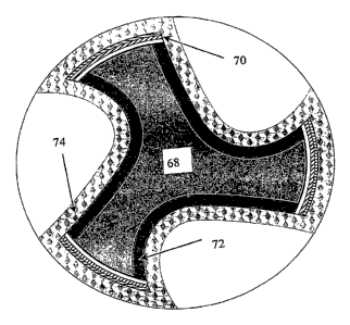
[0067] FIG. 11 shows the cross sections of an implant drill 68 through all
distinctive
stages (a-d)of the surface engineering process producing a triplex coating
architecture
CA 02652586 2008-11-17
WO 2007/136777 PCT/US2007/011952
27
shown in FIG. 8c on a rotary dental instrument. FIG. lla shows the cross-
section of the
blank drill (before the flute is ground) coated with Ti/TiN/TiCN/TiC
multilayer gradient
coating 70. FIG. 11b shows the same tool after grinding which produces a
flute. FIG. 11c
shows the drill after the first stage of the second coating process, which
produces the
ionitrided layer 72 on the inner side of the flute, where TiN coating was
removed by
grinding. FIG. 11d shows the final product, a triplex coated drill, having the
top segment
TBCN low friction anti-galling coating 74, which overlays the TiN on the outer
side of the
flute and ionitrided layer on the inner side of the flute.
[00681 In one of the preferred embodiments, a steel substrate has a bottom
bondcoating
segment of several vapour deposited layer pairs and is subsequently removed
from the
vacuum chamber of the filtered cathodic arc plasma depositing device and
annealed or heat
treated in vacuum or in a low pressure inert gas at a temperature between 900
C and
1100 C by usual methods, followed by quenching in nitrogen or nitrogen/argon
atmosphere
and tempering at 150 C to 400 C. The coated and heat treated substrate then
can be
sharpened or ground to prepare a necessary cutting shape blade or flute. After
this step, the
substrate is cleaned by applying at least one finishing method selected from
the group
consisting of sandblasting, chemical cleaning, electrolytic cleaning,
grinding, polishing,
= vibratory tumbling and ion etching to produce a cleaned substrate. The
cleaned substrate
the subjected to a subsequent coating deposition process to apply the overlay
low friction,
anti-galling coating, which reduces the stickiness between the rotary tool
surface and the
counterpart. The low friction coating is selected from the group containing
carbides, carbo-
nitrides, borides, and carbo-borides with an excessive amount of amorphous
carbon
forming a DLC type matrix. It can also be a doped or un-doped DLC layer. The
hydrogenated DLC can be used for further reduction of the friction and
stickiness between
the instrument and the counterpart.
CA 02652586 2008-11-17
WO 2007/136777 PCT/US2007/011952
28
TABLE 1
Item # Metal Layer Ceramic metal compound layer in combination with
the metal, having desired wear resistant properties
1 Ti TiC, TiN, Ti(CN), Ti(OCN)
2 Zr ZrC, ZrN, Zr(CN), Zr(OCN)
3 = V VC, VN, V(CN), V(OCN)
4 Cr CrN, CrC, CrCN
Hf HfN
6 Mo MoN
7 Nb NbN, NbC
8 w WC
9 Ti-Zr alloy TiZrC, TiZrN, TiZr(CN), TiZr(OCN)
Ti-Cr alloy TiCrC, TiCrN, TiCr(CN)
11 V-Ti alloy VTiC, VTiN, VTi(CN)
12 Ti,Mo TiMoN
13 Ti,A1 TiAlN, TiAION
14 Ti, Al, Si TiAlSiN
Ti, Nb TiNbN
16 - Al AIN, A1203
17 Ti,Cr (Ti,Cr)B2
18 Ti TiB2
19 Ti,A1 = (Ti,A1)B2 '
[00691 Table 2 lists the preferred metals and alloys used to obtain the
appropriate top
segment nanostructured coating having low friction and anti-galling properties
in
conjunction with the bottom bondcoating segment.
CA 02652586 2008-11-17
WO 2007/136777
PCT/US2007/011952
29
TABLE 2
Item # Elemental Amorphous matrix Nanocrystalline
composition composition filling phase
composition
1 C Hydrogen free None
single layer DLC
2 C Hydrogen free None
multilayer DLC,
consisting of iC
sublayers with
different ratio of
sp3/sp2 bonds and
having different
hardness
3 iCH Hydrogenated DLC None
4 Transition Me doped DLC MeC
metal+C =
Ti,B,C Ti, B doped DLC TiC, TiB2, B4C
6 Ti,Zr,B,C Ti, Zr, B doped TiC, TiB2, B4C,
DLC ZrB2, ZrC
7 B,C B doped DLC B4C
8 B,C,H B doped B4C
= hydrogenated DLC
9 Ti,A1,Cr,Mo, Ti,.A1,Cr,Zr,Mo, B TiC, TiB2, B4C,ZrC
Zr,B,C,H doped hydrogenated TiC, (Ti,A1)B2,
DLC (Ti,Cr)B2, ZrB2,
Mo2C
CA 02652586 2008-11-17
WO 2007/136777 PCT/US2007/011952
[0070] The top layer can be also composed of cermet based material doped
with
lubricious metals such as silver, gold or a like. In this case the cermet
provides a wear
resistant tough anti-galling matrix with embedded lubricious metallic
inclusions. One
example of such coating is TiCN+Ag. Other examples include multiphase
nanocrystalline
carbides, carbo-nitrides, and bonides with addition of silver and / or gold
metallic
inclusions. Alternatively, the lubricous metal coatings such as silver can be
applied over
the bondcoating layer as a replacement for DLC type top low friction segment,
forming
Me/MeN+Ag coating architecture. Another alternative solution for the low
friction coating
segment can be solid lubricant materials such as MoS2 and WS2. These solid
lubricant
compounds can be embedded into a hard coating matrix either in the bottom
bondcoating
or top coating segment. One example of such a nanocomposite self-lubricating
coating is
Ti/TiCN multilayer matrix with embedded WS2 inclusions. This coating can be
prepared
by hybrid LAFAD-UBM process. In this process the LAFAD will be equipped with
two
targets made of transition metals such as Ti, Cr, V or a like or their alloys.
The magnetron
targets will be WS2 or MoS2. The reaction gas atmosphere will be formed by
nitrogen or
mixture of nitrogen with methane or other HC gas, while argon will be supplied
in the
vicinity of magnetron targets as a sputtering gas. The resulting coating will
consist of hard
cermet matrix with embedded MoS2 or WS2 solid lubricant phases.
[00711 The preferred substrate surface temperature during the cathodic arc
plasma
deposition steps is between 100 and 500 C. In some cases the temperature of
the substrates
to be coated cannot exceed a certain value; otherwise it can have a
detrimental effect on the
bulk metal properties. For example, temperature must be controlled in coating
of rotary
instruments made of cold work hardening steel such as AISI 300 series or NiTi
nickel-
titanium alloy. In case of instruments made of AISI 300 series stainless steel
the bulk metal
properties cannot be restored by appropriate post-deposition heat treatment.
In the case of
dental instruments such as endofiles made of NiTi shape memory alloy the
temperature
must not exceed 100 -300 C during the coating process, otherwise post-
deposition thermal-
mechanical treatments are necessary to restore the shape memory properties of
the
instrument. In some cases the properties of the NiTi may not be able to be
restored at all if,
for example, the instrument is exposed to too high of a temperature for too
long a period
of time. For NiTi type substrates with thin part diameters exposure to
temperatures as high
CA 02652586 2008-11-17
WO 2007/136777 PCT/US2007/011952
31
as 350 C or five minutes can degrade the shape memory effect of the material.
At 300 C
this loss can occur in 20 minutes, one hour at 250 C, or 2 hours at 200 C.
Both the coating
of the substrate material, and post deposition heat treatment are meant to
maintain the
stiffness or increase the stiffness properties of the substrate when used in
many
applications. It is also important to notice that some of the coating layers,
specifically the
free carbon contained top low friction segment coatings are extremely
sensitive to high
temperature treatment in both oxidizing and reducing environments. Therefore
heat
treatment of these coatings is as problematic as the bulk metal substrates. In
all these cases
' precise thermal management of the substrate in the vacuum plasma coating
deposition
process is required.
[00721 In a deep vacuum, the only cooling mechanisms are radiation and
conduction
cooling. Using the pulsing mode of the LAFAD plasma source the precise thermal
management of the tiny instruments such as endofiles can be achieved by
periodically
interrupting the exposure ofthe instrument substrate to the vapor plasma
environment. This
can be accomplished by using a magnetic shutter which effectively closes the
path of the
vapor metal plasma flow toward the substrates to be coated. When the magnetic
shutter is
closed (the deflection magnetic system OFF) only the near neutral metal vapor
flow
generated by the EBPVD source or magnetrons will be deposited on the metal
instrument
substrate, bringing a negligible amount of heat, while the substrate is losing
the thermal
energy by radiation cooling. This allows the temperature of the substrate to
be controlled
during the deposition of the cermet coating at a desirable level and not to
exceed the
temperature which damages the bulk metal properties.
[00731 The duration time and duty cycle of the filtered arc source
operation effectively
determine the substrate temperature in the vacuum plasma deposition process of
the cermet
coating, while the total coating time determines the coating thickness. The
periodic
interruption of substrate exposure to metal vapor plasma flow can also be
achieved by
periodic turning on and off the plasma sources. Since substrate temperature is
a very
important parameter in determining film properties, special attention is paid
to in-situ
monitoring of substrate temperature using a high-precision pyrometers and
built-in
thermocouples.
CA 02652586 2008-11-17
WO 2007/136777 PCT/US2007/011952
32
[0074] In addition, the substrate rotary tools such as endofiles are
installed into blocks
having a high thermal capacity for heat transfer, these blocks may be made of
copper,
aluminum, or similar alloy, then a heat sink paste is used to provide
appropriate heat
transfer during the coating deposition process as shown in FIG. 9. If the
thermal flux
conveyed by the plasma to the instrument surface is q[W/cm2] and the heat
capacity of the
tool is Ct-----ct x int, where ct is specific heat capacity of the metal
substrate, mt is mass of the
instrument; then the pulse period tp, when the instrument can be exposed to
the vapor
plasma deposition environment can be estimated as following:
tp=(Ct x (T.-T0))/q, (1)
where To is initial temperature of the instrument, which can be estimated as
room
temperature, T. is maximum temperature to which the instrument can be heated
during
vapor plasma deposition treatment. More thorough calculations must be provided
to take in
to account the radiation and conduction cooling fele instruments during pause
time in the
cycled deposition process. In this case the expression (1) still gives a first
rough estimate of
the maximum plasma exposure time. The total coating deposition process time is
limited
by the heat capacity of the substrate holder blocks made of copper, aluminum
or other
metal with suitable high thermal conductivity and heat capacity. When the
temperature of
substrate holder block Tb>(2/3)Tm the coating deposition process must be
interrupted until
the temperature of the substrate holder block drops below this level.
[0075] Another way of trimming the substrate temperature below the value
detrimental
to bulk metal properties, is placing a substrate in a metallic or wire cage,
which can
effectively reduce the heat of the substrate due to intense ion bombardment as
illustrated in
FIG. 9. It is also possible to add Hydrogen or Helium gas to the chamber at
certain
intervals to reduce the chamber and substrate temperatures.
[0076] The technology described in this invention can be applied to wide
variety of
applications in forming and cutting tools, machine parts, medical and dental
instruments
and many others. In dental instruments applications it can be applied to both
handle
instruments such as regular and ultrasonic scalers, scalpels, needleholders
and to rotating
instruments such as root canal endofiles, dental drills and burs. The
substrate dental
CA 02652586 2008-11-17
WO 2007/136777
PCT/US2007/011952
33
instruments can be made of different type of steel and metal alloys. The
preferable type of
steel or metal alloy for different kind of dental instruments is shown in
Table 3.
Table 3. Description of the metal alloys preferably used for the dental
instruments of this
invention.
Item Name of Preferable type Manufacturer Composition of substrate metal
No. dental of steel or metal of substrate
instrument alloy metal
1 Scalers and 1-- 440A, 440C, 1- Carpenter 440 series is high chromium
Currettes 440XH, 440E- 2-Sandvic by bearing steel;
Se; BiolineTM 440E-Se composition:
2- 1RK91, brand 0.95/1.20 C, 1.25 Mn, 0.040 P,
13C26, 0.15 S or Se min., 1.00 Si,
4C27Mo2, 16.00/18.00 Cr, 0.60 Mo, Bal. Fe
20AP
2 Ultrasonic 1-17-4 family, 2-Sandvic by TrimRite composition:
13-8;TM C, 1.00
Mn, 0.04 P,
scalers Bioline TM
2- TrimRite, 0.03 S, 1.00 Si, 13.50/15.00 Cr,
Trinamet, 420, brand 0.25/1.00 Ni, 0.40/1.00 Mo, Bal.
1RK91, 13C26, Fe;
4C27Mo2, Trinamet composition:
20AP, Type Analysis Carbon
(Maximum) 0.30 % Manganese
(Maximum) 1.00 % Phosphorus
(Maximum) 0.040 % Sulfur
(Maximum) 0.030 % Silicon
(Maximum) 1.00 % Chromium
12.00 to 14.00 % Molybdenum
1.00 to 3.00 % Copper 2.00 to
3.00 % Iron Balance
=
3 Implant 1-17-4 family, 2-Sandvic by 1RK91 composition:
d 300 series;
BiolineTM C+N 50.05, Cr 12.0, Ni 9.0, Mo
rills
2-1RK91, 4.0, Ti 0.9, Al 0.30, Si 0.15, Cu
1 2 brand , 2.0
3C6,
4C27Mo2, 20AP 7C27Mo2 composition:
C 0.38, Si 0.4, Mn 0.6, P max
CA 02652586 2008-11-17
WO 2007/136777
PCT/US2007/011952
34
0.025, S max 0.01, Cr 13.5, Mo
1.0
20AP composition:
C 1.0, Si 0.2, Mn 0.4, P max
0.03, S 0.05, Cr max 0.10, Ni
max 0.10, Mo max 0.03, others
Pb 0.2
4 Dental burs Cemented Brasseler,
carbide Sybron
Root canal 1-17-4, 13-8; 3-Sandvic by NiTi shape memory alloy has near
endofiles 2-NiTi BiolineTm equiatomic
50%/50%
3- TrimRite, brand
Nickel/Titanium composition
Trinamet, 420,
1RK91, 13C26,
4C27Mo2, 20AP
Example 1. Stainless steel endofiles with multilayer gradient
TiCr/TiCrN+TiCrCN+TiBC
coating.
[0077] A set of endofiles made of 17-4 stainless steel were installed into
the substrate
holders positioned on the satellites of the rotating table of surface
engineering system
shown in FIG.1. The following process parameters were used for the deposition
of
TiCrN/TiCr-TiCrCN bottom segment and transitional layer by LAFAD plasma source
equipped with two (opposite) Ti and Cr targets. The arc currents were set on
approximately
100 amperes for both Ti and Cr targets. The auxiliary arc discharge current
was set on 150
amperes during argon ion cleaning stage and then reduced to 40 amperes during
coating
deposition stage. The substrate temperature did not exceed 300 C. An Advanced
Energy
Industry MDX-II power supply coupled with a Sparkle-V accessory unit was used
as a bias
power supply. The bias voltage was set at 250 volts during an ion cleaning
stage followed
by 1000 volts during 2 mins of a metal ion etching stage. The pulse frequency
during ion
cleaning/etching stages was set at 48 kHz with 90% duty cycle (reverse pulse
time 2tts).
The bias voltage during coating deposition stage was set at 60 volts DC. The
TiCrN/TiCr
CA 02652586 2008-11-17
WO 2007/136777 PCT/US2007/011952
multi-layer nanolaminated coating was deposited at 4x10⁻² Pa gas pressure with
nitride
sublayer being deposited in nitrogen reactive atmosphere and metallic sublayer
being
deposited in argon. Each bilayer in TiCrN/TiCr multilayer architecture was
deposited
during 10 min with 7 min dedicated to TiCrN and 3 min to TiCr sublayers. The
rotation
speed of the substrate platform was set at 9 rpm, which corresponds to a 3-4
nm bi-layer
thickness in the (Ti based/Cr based) nanolaminated architecture, taking into
account an
approximately 1.5 gm/hr deposition rate for TiN and 1 gm/hr for CrN coatings
deposited in
single (one fold) rotation mode. The pure nitrogen was gradually changed to
N2/40%CH4
during a 40 min deposition of the intermediate TiCrCN layer. The preliminary
set of
samples was prepared with a TiCrC upper tribological segment deposited by
LAFAD, on
top of the transition TiCrCN layer using acetylene as a reactive gas at
pressure of 5mTorr.
During deposition of the bottom segment TiCr/TiCrN+TiCrCN coating the magnetic
deflecting system was set in pulse mode with 50% duty cycle and frequency of
0.1Hz,
which result in 5 s deposition time followed by 5s cooling time at each bi-
period. The
thickness of the bottom segment coating was 0.2 gm. Additional samples were
produced
with an upper layer consisting Of TiBC nanocomposite cermet deposited by a
hybrid
filtered arc-unbalanced magnetron process. In this case both primary cathodic
arc sources
of LAFAD plasma source were equipped with Ti targets for generating titanium
vapor
plasma flow. The magnetron power density was set at approximately 5.5 W/cm2. A
small
amount of reactive gas (methane) was added to argon at a total gas pressure of
0.2 Pa. For
deposition of nanolaminated TiBC/iBC (NL) coating architecture the deflecting
magnetic
field of the LAFAD plasma source was cycled on for 5s and off for 25s. This
setting
resulted in the TiBC coating architecture consisting of TiBC sublayer of
approximately 4
nm thickness followed by 1 nm of B4C sublayer per each bi-period across 1 gm
of top
segment TiBC coating. After the deposition process was finished the substrates
were
discharged from the chamber. It was found that substrate stainless steel files
do not lose
their stiffness after the multilayer coating process.
CA 02652586 2008-11-17
WO 2007/136777 PCT/US2007/011952
36
Example 2. NiTi endofiles with anti-friction carbon diamond-like coating.
[0078] A set of endofiles made of NiTi nickel-titanium alloy were placed in
the copper
blocks and installed in the substrate holders, positioned on the satellites of
the rotating
table of surface engineering system shown in FIG.1. The thermal transfer or
"thermal sink"
compound ("Thermal Compound" Part # 120-8, manufactured by Wakefield
Engineering
Inc. of MA) was placed in the hole to reduce the thermal contact resistance
between the
instrument and the copper block so that instruments can be provided with
substantial
thermal conduction cooling during vapour plasma deposition process.
[0079] The following process parameters were used for the deposition of DLC
low
friction carbon coating using two LAFAD plasma sources, one (for bondcoating
layer)
equipped with two Ti targets and another one equipped with two graphite
targets. The ion
cleaning step was performed in argon ionized in auxiliary arc discharge,
created between
primary cathodes of one LAFAD plasma source as an emitter of electrons and
auxiliary
anodes installed around the substrate table in a main vacuum chamber. The
auxiliary anode
current was 100 amperes, the argon pressure was 0.5mtorr and bias voltage,
created
autopolarization of substrates under 13.56MHz voltage provided by a RF
generator, was
200 volts. The ion cleaning step lasts 2 min, which protects the substrates
against
overheating. After the ion cleaning step the deflecting magnetic field of
LAFAD source
with Ti targets was turned ON for deposition of the bond coating Ti/TiN/TiC
layer. It was
started from depositing of the 10 nm Ti layer followed by deposition of 30 to
50 nm of TiN
layer in nitrogen and topped with 100 nm of TiC layer deposited in a methane
reactive gas
atmosphere. The gas pressure during deposition of the bondcoating is 0.5mTorr,
the auto-
bias voltage is 50 volts.
[00801 After deposition of the bondcoating layer the LAFAD source with Ti
targets
was turned OFF and substrates were subjected to cooling step in helium or
hydrogen at the
pressure ranging from 1 to 10 mTorr. The duration of cooling step ranging from
10 min to
1 hr or more, depending upon thermal capacity of the substrates to be coated
and substrate
holder blocks. After the cooling step, the chamber was pumped down to
0.01mTorr and
other LAFAD source with graphite targets is turned ON. The 13.56 MHz RF bias
power
supply was connected to the substrate table instead of DC pulse bias power
supply, used
CA 02652586 2008-11-17
WO 2007/136777 PCT/US2007/011952
37
during deposition of cermet bond coating bottom segment. The substrate auto-
bias during
this stage was set at -50 volts. In addition the high voltage pulses having
2.5kV amplitude,
25 gs width and 600 Hz repetition frequency were applied subsequent to the low
auto-
polarization bias voltage. During the DLC deposition step the LAFAD deflecting
field was
periodically turned off for 10 s and turned on for 5 s which results in the
plasma deposition
and heating of substrates with subsequent cooling. This approach is capable of
precise
thermal management of substrates in vapor plasma deposition processes. After 1
hr of DLC
coating deposition step the LAFAD filter is turned off and substrates are
discharged from
the vacuum chamber. It is found that with approximately 1 p.m of DLC coating
the NiTi
endofiles fully restored their shape memory, while torsional fatigue life was
improved up to
200% due to reduction of friction and stickiness to the counterbody (bovine).
Deposition of
the top DLC layer having amorphous structure also results in substantial
improvement of
corrosion resistance by effectively filling the holes, voids and other
imperfections and
defects both on the substrate surface and in the bottom cermet layer,
preventive it against
pitting corrosion attacks.
Example 3. Endodontic files made of 17-4 stainless steel with two segment
cermet-DLC
coating.
[0081] A set of blank endofiles made of 17-4 stainless steel is cleaned by
vibratory
tumbling followed by ultrasonic cleaning dried and then loaded in the surface
engineering
system shown in FIG.1. The surface finish of the blank endofile after cleaning
is better than
Rrns<20nm. The first bondcoating segment consisting of TiZr/TiZrN multilayer +
TiZrCN
transition layer + TiZrC top layer is deposited on the blanks. The coating
deposition
process is performed using the LAFAD plasma source with Ti and Zr targets
installed into
opposite primary cathodic arc sources. The coating deposition parameters are
largely the
same as described before in Example 1. The coating thickness is 2 gm. After
finishing the
deposition of the bondcoating segment the substrates endofiles are removed
from the
chamber and subjected to heat treatment to restore the bulk mechanical
properties, the
primary of which is to retain the hardness and stiffness properties. After
heat treatment the
coated blanks are subjected to grinding and polishing treatment to make a
flute with a
cutting edge. As a result of this step the outer side of said flute remains
coated with a 2pm
CA 02652586 2008-11-17
WO 2007/136777 PCT/US2007/011952
38
thick bottom bondcoating segment and the other (inner) side of said flute is
uncoated,
while the very tip of the cutting edge is entirely made of the bondcoating
multilayer cermet,
having a hardness of H >25GPa. This step forms a cutting flute with a metallic
underside
and a ceramic metal outer layer or top side. After that the instruments are
subjected to
chemical-mechanical vibratory tumbling which creates a fine surface finish on
the
uncoated side of the flute and does not affect the outer side of the flute and
the very tip of
the cutting edge which are much harder than vibratory tumbling media. After
that the
substrate instruments are ultrasonically cleaned and placed in the copper
blocks positioned
on the satellites of the rotating table of surface engineering system shown in
FIG.1. The
thermal transfer or "thermal sink" compound ("Thermal Compound" Part # 120-8,
manufactured by Wakefield Engineering Inc. of MA) is placed in the hole to
reduce the
thermal contact resistance between the instrument and the copper block so that
the
instruments will have substantial thermal conduction cooling during vapour
plasma
deposition process. After ion cleaning and 5 min of exposure to TiZr metal
vapor plasma in
methane reactive gas atmosphere at lmtorr and -100V bias for deposition of
thin TiZrC
sublayer, the LAFAD source deflecting field is turned off and remains in
electron emission
auxiliary arc mode for ionizing gaseous plasma in the main chamber. At this
moment
methane flow rate is reduced to 4 sccm, argon is added as a main balance gas
to reach
lmtorr operating pressure, two unbalanced magnetrons with B4C targets are
turned on and
high voltage (12 kV) pulse bias is imposed on the substrates to provide boron-
carbon ion
implantation of the uncoated and coated sizes of the flute. This stage
continues for 10
minutes followed by deposition of nanolaminated TiZrBC coating containing
large
amount of free amorphous carbon by periodically exposing the substrates to
TiZr metal
vapor flow when deflection magnetic field of LAFAD source is turned on and
continuous
exposure of the substrates to B4C magnetron sputtering flow and additional
hydrocarbon
plasma flow at -50 volts bias. This results in deposition of a low friction
non-stick TiCrBC
top coating segment, which effectively encapsulates the smooth metallic
surface of the
inner side of the flute and provides large improvement of fatigue life by
securing low
torque momentum and preventing the development and fast propagation of surface
microcracks. At the same time this coating design has demonstrated cutting
efficiency by
retention of the wear and corrosion resistant low friction anti-galling dual
ceramic cutting
CA 02652586 2008-11-17
WO 2007/136777 PCT/US2007/011952
39
edge of the flute. Using 3MS reactive gas in addition to nitrogen during
deposition of the
top low friction segment coating results in TiCrBSiCN composition which
further
improves the corrosion resistance and cutting efficiency ofthe entire surface
engineering of
this type of dental instruments.
Example 4. Endodontic files made from NiTi alloy with 2-segment cermet+DLC
coating.
[00821 In this process the blank endofiles without flutes made of NITINOL
or
50/50at% NiTi alloy are subjected to deposition of a relatively thick
TiCr/TiCrN/TiCrCN/TiCrC multilayer gradient cermet coating 21-1,M thick at the
first stage
of the surface engineering process. During deposition of the bottom bond
coating segment
the temperature of the endofile substrates can reach up to 500 C, which
effectively erases
the shape memory properties. After this stage the coated blanks are removed
from the
LAFAD surface engineering chamber and subjected to annealing heat treatment
stage.
During this stage the coated blank files are subjected to 30 min heating at
1100 C in
nitrogen (99.995 purity) followed by rapid cooling by immersing the boat with
files into
ice. After annealing the coated blank files are subjected to thermal-
mechanical treatment
stage consisting of grinding by fine diamond wheels in a multi-step grinding-
tempering
process. Alternatively, after annealing and rapid quench the files can be
subjected to
tempering at temperatures ranging from 400 to 650 C for time duration ranging
from 15
min to 2 hrs. During this process the files are subjected in turn to grinding
and tempering in
a tempering furnace which allows restoring its shape memory properties. After
this stage
the files, which now have a flute are cleaned by mild vibratory tumbling and
loaded second
time in the LAFAD coating chamber for the subsequent deposition of hydrogen
free DLC
coating. This process is provided by LAFAD plasma source shown in FIG. 1,
which is
equipped with two graphite primary cathodic targets. The substrate endofiles
are installed
with double rotation capability into copper blocks with thermal sink compound.
No plasma
creating gases are used in this process and the chamber pressure during DLC
process is
measured at about 0.01 mtorr. The substrates are subjected to floating bias
potential with
superimposed high voltage pulses of 2 kV amplitude, 25 Its duration and 1000
Hz
repetition frequency. The duration of this dual filtered arc deposition
process is 4o min
resulting in deposition of 0.25 jAm DLC layer, which overlays the bottom bond
coating
CA 02652586 2013-05-21
cermet layer on the outer side of the flute and uncoated NiTi alloy on the
inner side of the
flute. The hardness of the DLC layer deposited on NiTi alloy was measured by
means of
nanoindentation as 25 GPa. The cumulative compressive stress in combined
cermet+DLC
coating was measured as about 3 GPa.
[0083] A novel coating is described that protects the coated surface
against wear and
corrosion while providing a low friction, anti-galling surface. In the
exemplified
embodiment, this novel coating architecture of a multilayer metal/ceramic
bondcoat topped
with a non-friction, anti-galling top coat is applied to rotary tools for
dental and medical
applications. It is important to note however that the subject coating can be
effectively
applied to other dental and surgical instruments including, but not limited
to, saw blades,
scalers, curettes, scissors, razorblades, scalpels, orthodontic components,
burs, and
implants. Additionally, the subject coating and the method of temperature
control
described for applying the coating are intended to be used for coating
ultrasonic cutting,
debriement, surgical, and periodontal therapy tools or instruments both of
Piezo and
Magneto Restrictive types for dental and medical applications. Finally the
coatings and
methods of the subject invention can be applied to other industries, such as
the aerospace
industry, the automotive industry (for use on, for example, gears, bearings,
combustion
engine components such as pistons .and piston rings, valves etc.) and other
cutting and
forming tools industries (for example, for use on dies and molds).
[0084] It is understood that the foregoing examples are merely illustrative
of the
present invention. Certain modifications of the articles and/or methods may be
made and
still achieve the objectives of the invention.
Accordingly, the scope of the claims should not be limited by the embodiments
set forth
in the examples, but should be given the broadest interpretation consistent
with the
description as a whole