Note: Descriptions are shown in the official language in which they were submitted.
CA 02652971 2008-11-21
WO 2007/135161 PCT/EP2007/054971
1
Image sensor circuit
BACKGROUND OF THE INVENTION
FIELD OF THE INVENTION
The present invention is related to an image sensor including a CMOS
image sensor with light sensitive pixels arranged in rows and columns and a
readout circuitry.
Only recently CMOS image sensors are beginning to enter the field of
professional cameras, for example cameras for TV productions or movie
productions. Until then those cameras were equipped with CCD image sensors.
CMOS image sensors offer a higher readout speed when compared with CCD
image sensors. However, until recently it was not possible to achieve the same
high number of pixels in a CMOS image sensor as could be produced with CCD
image sensors. The resulting resolution of CMOS image sensors was too low for
professional cameras. Today's manufacturing techniques are capable of
producing CMOS image sensors having similar numbers of pixels as CCD image
sensors.
CMOS image sensors can be produced at lower costs than CCD image
sensors. Further, CMOS image sensors can achieve higher frame rates due to
the higher readout speed that can be achieved. Yet further the noise of CMOS
image sensors is equal or less than the noise of CCD image sensors. Images
taken with CMOS image sensors appear crisper, brilliant, and, due to the
higher
readout speed, fast movements do not appear smeared. Another advantage of
CMOS image sensors is the possibility to integrate other circuitry on the
sensor
using the same technology.
DESCRIPTION OF THE PRIOR ART
In the US 5,742,042 B1 a photodiode sensor circuit is described, wherein a
readout circuitry includes a correlated double sampling circuit, i.e. a CDS
circuit,
CA 02652971 2008-11-21
WO 2007/135161 PCT/EP2007/054971
2
for elimination of pattern noise. The CDS circuit comprises a capacitor, a
clamping transistor and a transfer gate.
A circuit diagram with a CMOS image sensor circuit and a CDS circuit is
described in the US 5,969,758 B1. In the CDS circuit only switched capacitors
are
used. In an additional CDS circuit described in the US 6,320,616 B1 capacitors
with accompanying switches are used.
SUMMERY OF THE INVENTION
It is desirable to provide an image sensor circuit with a readout circuitry
for a
CMOS image sensor capable of high readout speed. It is also desirable to
provide a readout circuitry for a CMOS image sensor allowing for a high number
of pixels to be addressed. It is yet desirable to provide a readout circuitry
for a
CMOS image sensor having a low noise figure.
The invention suggests an image sensor circuit with a readout circuitry as
claimed in claim 1. Advantageous developments and embodiments of the
invention are presented in the dependent claims.
According to the invention, an image sensor circuit includes a CMOS image
sensor with light sensitive pixels arranged in rows and columns and a readout
circuitry, wherein the readout circuitry itself includes storage means with a
CDS
stage for storing signals read out from the pixels at two different time
instants
between two subsequent reset phases and an analogue-to-digital converter. The
CDS stage comprises a subtracting means for subtracting the stored signals
from
each other, wherein the result of the subtraction is fed to the analogue-to-
digital
converter as a differential signal. The CDS stage and the analogue-to-digital
converter are generated as differential CDS stage with a differential output
signal
and as a differential analogue-to-digital converter for converting the
differential
signal.
The balanced or differential design provides a good rejection of crosstalk,
common mode offsets. In particular, crosstalk of clock signals is reduced.
CA 02652971 2008-11-21
WO 2007/135161 PCT/EP2007/054971
3
Preferably, the differential signal is fed from the CDS stage to the analogue-
to-digital converter via a differential buffer stage. The differential buffer
stage is
used in order to decouple the CDS stage from the analogue-to-digital
conversion
stage and, as a result, to allow for high clock rates of the analogue-to-
digital
converter, corresponding to a high pixel rate and thus a high frame rate.
In one embodiment the differential buffer stage comprises transistors in a
source follower configuration.
In another embodiment the differential buffer stage comprises single-ended
operational amplifiers. Preferably, the differential buffer stage is provided
with two
buffer circuits, wherein each buffer circuit comprises a single-ended
operational
amplifier for one of two parts of the differential signal.
Preferably, the subtracting means comprises an amplifier, which is arranged
in a switched capacitor amplifier configuration
In a development of the invention the CDS stage is provided with a common
mode rejection stage. The CDS stage and the common mode rejection stage
preferably provide a linear signal characteristic. Preferably, the common mode
rejection stage is dynamically controlled.
In one embodiment of the invention the common mode rejection stage
comprises common mode feedback control circuits for controlling the common
mode operation point. Preferably, the common mode feedback control circuits
are
capacitively coupled.
BRIEF DESCRIPTION OF THE DRAWINGS
The invention will be explained in more detail using one embodiment,
illustrated in the figures.
CA 02652971 2008-11-21
WO 2007/135161 PCT/EP2007/054971
4
It shows:
Figure 1 an exemplary block diagram of an image sensor circuit with a readout
circuitry of the invention;
Figure 2 an exemplary circuit of a CDS stage;
Figure 3 an exemplary circuit of a differential buffer stage; and
Figure 4 an exemplary structure of the readout circuitry showing a signal
path.
DETAILED DESCRIPTION OF THE INVENTION
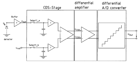
Figure 1 shows an exemplary block diagram of an image sensor circuit
including a CMOS image sensor with light sensitive pixels arranged in rows and
columns and a readout circuitry according to the invention. The readout
circuitry
includes storage means with a differential CDS stage for storing signals read
out
from the pixels at two different time instants between two subsequent reset
phases, a differential buffer stage and a differential analogue-to-digital
converter.
The CDS stage comprises a subtracting means for subtracting the stored signals
from each other, wherein the result of the subtraction is fed to the analogue-
to-
digital converter as a differential signal via the differential buffer stage.
The
subtracting means comprises a differential amplifier.
In particular, the CDS stage performs a correlated double sampling in the
analogue domain. An initial signal, also referred to as dark value is stored
in a
first capacitor. In the figure, the initial value is denominated Uref. A
signal
corresponding to the light integrated in a pixel during exposure after reset
of the
pixel is stored in a second capacitor. This signal is also referred to as
bright value
and is denominated Uout. The differential amplifier subtracts the bright value
from
the dark value and outputs the result of the subtraction as UCDS+ and Ucps_ to
a
differential driver or buffer stage. The differential analogue-to-digital
converter is
connected to the output of the differential buffer stage.
As a result, the CDS stage is decoupled from the analogue-to-digital
conversion stage by the differential buffer stage. The decoupling allows for
high
clock rates of the analogue-to-digital converter corresponding to a high pixel
rate
CA 02652971 2008-11-21
WO 2007/135161 PCT/EP2007/054971
and thus a high frame rate. The differential buffer stage comprises at least
one
single-ended operational amplifier.
During operation at first a reference value or dark value is stored. The dark
5 value can be the reset value of the image sensor or can be fed to the
circuit
externally. Thereafter the image sensor is exposed. The signal from the
exposed
image sensor or bright value is also stored. The stored values are subtracted
from each other in the CDS stage. Subtraction can be performed, e.g. by a
differential amplifier. In a preferred embodiment the reset value of the CMOS
image sensor is used as the dark value. Depending on the CMOS sensor circuitry
it may be necessary to store the reset value in an additional storage means,
for
example a capacitor. The calculated difference value may be amplified or
buffered in the CDS stage. In the case of high numbers of pixels to be read
the
required bandwidth of the readout circuit can be very high. The same applies
to
the output of the CDS stage, in case it is also used as a buffer. Since a
certain
time is required in the CDS stage for the signals and transients to settle as
well
as to ensure a required minimum dynamic the bandwidth of the CDS stage is set
to a predetermined value.
As an example, in order to provide a pixel signal having an 8-bit resolution
the CDS stage must provide a useful dynamic range of 8 bit * 6 dB/bit = 48 dB
at
the desired operating frequency. Typically, amplifiers exhibit a relationship
between gain and bandwidth which has to be considered. In order to determine
the 3dB roll off frequency the following equation can be used:
2* Tr* GBW = v* f 3dB,
wherein v corresponds to the gain, f_3dB is the 3 dB roll off frequency and
GBW
is the gain-bandwidth product of the amplifier. The required game-bandwidth
product is determined by the pixel clock. For an image sensor having 1480 by
1920 pixels and a frame rate of 100 Hz the required gain-bandwidth product can
be calculated as GBW = 100 Hz * 1480 * 1920 = 284 MHz. In order to provide
enough dynamic for later image processing a resolution of 12 bit or 16 bit is
desired. The gain of the amplifier can then be calculated as:
12bit6 dB l bit
v = 10 21dB = 3981.
CA 02652971 2008-11-21
WO 2007/135161 PCT/EP2007/054971
6
The 3 dB roll off frequency of the CDS stage amplifier can then be
calculated as:
dB = 2.7c = GB W = 448kHz . f3 V
At the same time the noise of the CDS stage must not be higher than
allowed for the required dynamic range, in this example 72 dB or 12 bit.
Analog
circuits in CMOS process technology having structural sizes equal to or
smaller
than 0.5 pm and 3.3 V supply voltage allow for a useful signal swing of 1.8 V.
Given these values the maximum noise allowed for the amplifier can be
estimated as follows:
DR = 20dB log VI"~
vn
wherein DR is the dynamic range, in this case 72 dB, determined by the desired
resolution. Vmax is the maximum useful signal swing, in this case 1.8 V and vn
is
the equivalent noise voltage. Solving this equation for the noise results in a
maximum admissible equivalent noise voltage of vn = 140 pV. A typical
operational amplifier having a 3 dB roll off frequency of 448 kHz does not
comply
with these requirements. The maximum admissible equivalent noise voltage of
140 pV corresponds to an equivalent noise power of 19.5 nV2. Noise powers of
this magnitude would reduce the sensitivity of a pixel in such a way that dark
areas of an image would not contain any useful information. The requirements
as
to sensitivity and speed set out by professional cameras can, therefore, not
be
fulfilled by a readout circuitry based on known, single CDS stages.
As mentioned above, according to the invention the readout circuitry is
provided with a differential design. In particular, the differential buffer
stage is
provided between the differential CDS stage and the differential analogue-to-
digital conversion stage. This differential buffer stage reduces the bandwidth
requirements of the CDS stage amplifier and hence reduces the noise of the
amplifier. The subtraction and high precision amplification is performed in
the
CDS stage. The differential buffer stage is provided for the high-speed
transmission of the so-treated signal to the analogue-to-digital converter. It
goes
without saying that the noise added by the differential buffer stage must be
lower
CA 02652971 2008-11-21
WO 2007/135161 PCT/EP2007/054971
7
than the reduction of the noise in the CDS stage by reducing the gain-
bandwidth
requirements of the CDS stage.
In figure 2 an exemplary circuit of a differential CDS amplifier will be
described. The exemplary circuit shown in the figure 2 is supplemented by an
output stage further increasing the open loop gain and thereby the accuracy of
the CDS amplifier. The exemplary circuit shown in the figure allows for
amplifier
designs having an open loop gain of more than 100 dB and being suitable for
applications requiring 16 bit resolution. Reference voltages V_ref1 to V_ref5
are
supplied to the circuit via a reference voltage network. In the figure the
reference
voltages are generated and distributed by transistors T3, T4, T5 and T6 in a
current mirror configuration to cascode-connected transistors T1 and T2.
The CDS stage is provided with a common mode rejection stage, wherein
the CDS stage and the common mode rejection stage provide a linear signal
characteristic. To this end, the common mode rejection stage is dynamically
controlled.
In particular, the common mode rejection stage comprises common mode
feedback control circuits CMFB, which are provided for controlling the common
mode operating point. In one embodiment the common mode feedback control is
capacitively coupled. The input stage of the CDS amplifier has a positive and
a
negative input Vin+ and Vin-. The positive and the negative inputs Vin+ and
Vin-
are connected to respective outputs of the imager providing the dark and the
bright values (not shown). A capacitive coupling network (not shown) may be
provided for connecting the outputs of the CDS amplifier Vout+ and Vout- to
the
input of the subsequent differential buffer stage (not shown). Offset
compensation
and subtraction are performed between the inputs and the outputs of the CDS
amplifier. It is important that the CDS amplifier stage provides low-noise
operation. Consequently, offset compensation and subtraction are performed at
a
lower speed.
CA 02652971 2008-11-21
WO 2007/135161 PCT/EP2007/054971
8
In order to transfer the signals acquired in the CDS stage to the analogue-
to-digital converter the differential buffer or driver stage is provided.
Figure 3 shows an exemplary buffer circuit of the differential buffer stage in
accordance with the invention. The buffer circuit shown in the figure is
provided
twice for each output of the CDS stage, i.e. for each of the two parts of the
differential signal. The respective inputs Vin+ of the two buffer circuits are
connected to respective outputs Vout+, Vout- of the CDS amplifier. The
positive
outputs Vout+ of the two buffer circuits are connected to the respective
inputs of
the differential analogue-to-digital converter. Depending on the design of the
imager, i.e. of the CMOS image sensor, a varying number of CDS amplifiers and
buffer stages can be provided on the imager chip. It is also possible to
couple a
number of CDS amplifiers to the imager via a bus-system. In this case a
decoder
and address network is provided for addressing the pixels of the imager. The
latter case requires higher bandwidth and higher speed in the CDS stage. The
maximum possible reduction in the bandwidth of the CDS stage and hence the
maximum possible reduction of the noise in the CDS stage is achieved by
combining each CDS stage with an associated driver or buffer stage. However,
an increased power consumption may be contemplated in this case. In order to
reduce the power consumption mixed architectures may be preferred.
In the exemplary buffer circuit transistors T17 and T18 form a differential
amplifier. T15 and T16 are arranged in the common current path of the
differential
amplifier and set the operating current. Transistors T11, T12 and T13, T14 are
arranged in respective cascode configurations with Vref3 being the fixed
potential
at the gate electrodes of T12, T14 and T16. Transistors T19, T20 and T21, T22
form respective cascodes that are connected with the drain electrodes of
transistors T17 and T18. The control electrodes of transistors T19, T22 and
T20,
T21 are connected to respective reference potentials Vref2, Vrefl. The control
electrode of T18, representing the negative input Vin-, is connected to the
output
of the buffer stage.
CA 02652971 2008-11-21
WO 2007/135161 PCT/EP2007/054971
9
Figure 4 shows an exemplary structure of a signal path of an image sensor
circuit according to the invention. In the figure, a basic pixel circuit
including a
photodiode PD, a reset transistor Q1, a capacitance CD, a source follower Q2
and a selector switch Q3 are shown. This basic pixel circuit is known from the
prior art. The basic pixel circuit is connected to a column line via the
selector
switch Q3. Parasitic capacitances of the column lines are shown as CsPa,te in
the
figure. Switches S1, S2 are provided for applying the signal read out from the
basic pixel circuit to respective storage or sample capacitances CS1, CS2. The
storage or sample capacitances CS1, CS2 can be reset by respective switches
S3, S4. The CDS amplifier shown in figure 2 is arranged in this figure in a
switched capacitor amplifier configuration including switches S6. S7, S8, S9,
S11
and S12 and capacitors CF1, CF2. Buffer circuits 16, 17 as presented in figure
3,
provide buffering for the respective positive and negative output of the CDS
amplifier. The buffer stages couple the differential signal coming from the
CDS
amplifier to a differential analogue-to-digital converter 21.
In the table below, figures for noise, power consumption and a maximum
resolution are given for an exemplary readout circuit according to the
invention.
The resolution of a CDS stage is generally expressed in terms of noise
equivalent
electrons. The capacitance of the image detector, for example of the blocking
capacitance of the photodiode, must be known for the calculations. The figures
are given for an imager produced in a 0.35 pm 3.3 V CMOS process. Further key
figures of the elements are given below:
Capacitance of the image detector CD = 2.0 fF
Sample capacitance of the CDS stage = 512 fF
Feedback capacitance of the CDS stage = 256 fF
Capacitive load at AD converter input = 2 pF
Frame rate = 100 Hz
Number of pixels in the imager = 1480 x 1920
Number of read out channels = 32
CDS stage without CDS stage with
Parameter differential buffer (prior differential buffer stage
art)
CA 02652971 2008-11-21
WO 2007/135161 PCT/EP2007/054971
Power consumption (one 10 mW 36 mW
read-out channel)
Equivalent noise
electrons (CDS stage + 11.5 4.3
buffer sta e
Maximum resolution 10 bit, limited by 16 bit
accuracy of settlin
The figures in the table are given for a worst case signal, in which a full
black and a full white pixel following each other are assumed. In the case of
a
monotonous grey-to-grey transition the noise values will be reduced.
5
The circuit according to the invention advantageously reduces the noise
created in the CDS stage. Further, the bandwidth of the readout circuit is
increased, thereby allowing for higher frame rates and/or numbers of pixels.
The
reduced noise allows for creating sensor arrangements having a higher number
10 of pixels and a high dynamic range. The improved sensor arrangements, i.e.
the
improved image sensor circuits, may be used for high definition TV as well as
for
professional cinematographic filming. Further fields of applications include
automotive, surveillance and medical applications in which high resolution and
high-speed image capturing is required.