Note: Descriptions are shown in the official language in which they were submitted.
CA 02653207 2008-11-21
DESCRIPTION
POWER CONVERTER
TECHNICAL FIELD
[0001]
This invention relates to power converters for the
vehicles of a railway, etc. More particularly, it relates to
a power converter in which semiconductor elements forming the
respective phase arms of the power converter are arranged on
the same plane of a cooler, so as to heighten the cooling
efficiencies of the semiconductor elements and to reduce the
wiring inductances thereof.
BACKGROUND ART
[0002]
As a prior-art power converter for a vehicle, there has
been one wherein, as indicated in JP-A-2001-238468 (termed
"Patent Document 1") by way of example, a plurality of
semiconductor units unitized for respective phases are attached
to one heat block by attachment screws so as to extend in the
traveling direction of the electric car, thereby to attain the
enhancement of a cooling efficiency and the reduction of a
circuit inductance.
Besides, as an apparatus which has attained the
reductions of inductances in the main circuit wiring lines of
a power converter, the enhancement of the reliability of
insulation, and the enhancement of a handling property, there
1
CA 02653207 2008-11-21
is one indicated in JP-A-2001-86731 (termed "Patent Document
2") .
[0003]
Such vehicular power converters indicated in Patent
Documents 1 and 2 have a configuration wherein IGBT modules
forming the positive-side arms and negative-side arms of the
power converter are arranged on a cooler so that the shorter
side of the IGBT modules may become perpendicular to the
traveling direction of the vehicle, and wherein a wind is blown
to the heat radiation section of the cooler by the travel and
movement of the vehicle, and the wind impinges against the heat
radiation section as a cooling wind, so that the cooler is
cooled.
[0004]
Patent Document 1: JP-A-2001-238468 (FIG. 1)
Patent Document 2: JP-A-2001-86731 (FIG. 1)
DISCLOSURE-OF THE INVENTION
PROBLEMS THAT THE INVENTION IS TO SOLVE
[0005]
In such prior-art power converters, however, the shorter
side of the IGBT modules forming the positive-side and
negative-side arms are located in a relationship perpendicular
to the flow of the cooling wind (that is, the traveling direction
of the vehicle ), so that a length from the windward to the leeward
is large with respect to the cooling wind, and the temperature
2
CA 02653207 2008-11-21
difference between the IGBT module at the windward and the IGBT
module at the leeward becomes large. Besides, since that area
of each IGBT module which is struck by the cooling wind is small,
the efficiency of cooling is inferior. Therefore, the wind
generated by the travel of the vehicle cannot be effectively
used as the cooling wind. In order to sufficiently cool the
IGBT module at the leeward, a cooling performance must be set
high, and a cooler of large heat radiation section or high
efficiency is necessitated. This has led to the problems that
enlargement in the size of the apparatus is incurred, and that
rise in the cost of the apparatus is incurred.
[0006]
This invention has been made in order to solve such
problems of the prior-art apparatuses, and it has for its object
to provide a power converter in which the areas of semiconductor
element modules forming positive-side arms and negative-side
arms as receive a cooling wind are ensured to be large, the
temperature difference between the semiconductor element
modules on a windward side and on a leeward side can be made
small, and the heat radiation section of a cooler can be made
small, whereby the smaller size and lower cost of the apparatus
have been permitted.
[0007]
Besides, this invention has for its object to provide a
power converter in which the inductances of circuits are
3
CA 02653207 2008-11-21
decreased by wiring structures suitable for the layout states
of semiconductor element modules, whereby the smaller size and
lower cost of the apparatus have been permitted.
MEANS FOR SOLVING THE PROBLEMS
[0008]
A power converter according to this invention consists
in a power converter for a vehicle, wherein a series circuit
of a positive-side semiconductor switching arm and a
negative-side semiconductor switching arm which are formed of
switching semiconductor elements is connected between a
positive potential side and a negative potential side of a DC
voltage supply; an output terminal is led out from a series joint
of the two sets of semiconductor switching arms; an anode of
the positive-side semiconductor switching arm is connected to
the positive potential side of the DC voltage supply, while a
cathode of the negative-side semiconductor switching arm is
connected to the n-egative potential side, -of the -DC voltage
supply; the series circuit of the two sets of semiconductor
switching arms is used as one phase component of the power
converter; all the switching semiconductor elements which form
the semiconductor switching arms are arranged on the same plane
of a cooler; and a cooling section of the cooler is configured
of a plurality of fins so that the switching semiconductor
elements may be cooled by a refrigerant which flows between the
fins; the switching semiconductor elements being disposed on
4
CA 02653207 2008-11-21
the same plane of the cooler so that longitudinal directions
of the semiconductor switching arms may become perpendicular
to a flowing direction of the refrigerant.
[0009]
Besides, in the power converter configured as stated
above, a wiring line which connects the anode of the switching
semiconductor element forming one (the positive-side)
semiconductor switching arm and the positive potential side of
the DC voltage supply employs one first flat conductor which
is common to all phases constituting the power converter; a
wiring line which connects the cathode of the switching
semiconductor element forming the other (the negative-side)
semiconductor switching arm and the negative potential side of
the DC voltage supply employs one second flat conductor which
is common to all the phases constituting the power converter;
a third flat conductor for each of the phases is employed as
a--wzring iine which connects -a cathode of- said ane
(positive-side) switching semiconductor element forming the
series circuit and. an anode of the other (negative-side)
switching semiconductor element; the first - third flat
conductors are made stacked parallel flat plates; and the third
flat conductor is arranged so as to be connected to the output
terminal with the cathode side striding over the anode of said
one (positive-side) switching semiconductor element as is
connected with the output terminal and with the anode side
CA 02653207 2008-11-21
striding over the cathode of the other (negative-side)
switching semiconductor element connected with the output
terminal.
ADVANTAGES OF THE INVENTION
[0010]
In accordance with the power converter of this invention,
the heat radiation section of a cooler can be made small in size,
and the price of the cooler can be suppressed low.
Moreover, since the inductances of circuits can be
lowered, a snubber circuit is dispensed with, the number of
components can be decreased, the reliability of the apparatus
can be heightened, the size of the apparatus can be reduced,
and the price of the apparatus can be suppressed low owing to
the decreased number of components.
BRIEF DESCRIPTION OF THE DRAWINGS
[0011]
[FIG. 1] It i-s a schematic circuit configuration diagram of a
power converter in Embodiment 1 of this invention.
[FIG. 2] It is an explanatory diagram showing the layout
configuration of switching semiconductor elements on a cooler
in Embodiment 1 of this invention.
[FIG. 3] It is a schematic circuit configuration diagram of a
power converter in Embodiment 2 of this invention.
[FIG. 4] It is an explanatory diagram showing the layout
configuration of semiconductor elements on a cooler in
6
CA 02653207 2008-11-21
Embodiment 2 of this invention.
[FIG. 5] It is a schematic circuit configuration diagram of a
power converter in Embodiment 3 of this invention.
[FIG. 6] It is an explanatory diagram showing the layout
configuration of semiconductor elements on a cooler in
Embodiment 3 of this invention.
[FIG. 7] It is a diagram showing a modification to the cooler
in the power converter in Embodiment 1 of this invention.
[FIG. 8] It shows an arrayal diagram of the semiconductor
elements of positive-side and negative-side arms and a diagram
of wiring circuits based on flat semiconductors, in a power
converter in Embodiment 4 of this invention.
[FIG. 9] It is a diagram of the wiring structures of the flat
conductors which connect the positive-side semiconductor
elements and the negative-side semiconductor elements, in the
power converter in Embodiment 4 of this invention.
[FIG. 10]- It is a diagram of the wiring structure between the
positive-side semiconductor elements and the positive
potential side of a power supply, in the power converter in
Embodiment 4 of this invention.
[FIG. 11] It is a diagram of the wiring structure between the
negative-side semiconductor elements and the negative
potential side of the power supply, in the power converter in
Embodiment 4 of this invention.
[FIG. 12] It is a diagram showing the stacked structure of the
7
CA 02653207 2008-11-21
flat conductors in the power converter in Embodiment 4 of this
invention.
[FIG. 13] It is a diagram for explaining the relationship
between current paths and wiring inductances in the power
converter in Embodiment 4 of this invention.
[ FIG . 141 It is an explanatory diagram of wiring paths and wiring
inductances in a prior-art apparatus.
[FIG. 15] It is an explanatory diagram of wiring paths and wiring
inductances in the power converter in Embodiment 4 of this
invention.
[FIG. 16] It is a wiring structure diagram and a wiring circuit
diagram of flat conductors which connect the positive-side
semiconductor elements and negative-side semiconductor
elements in the power converter in Embodiment 5 of this
invention.
[FIG. 17] It is a wiring structure diagram and a wiring circuit
diagram of flat conductors which connect the positive-side
semiconductor elements and negative-side semiconductor
elements in the power converter in Embodiment 6 of this
invention.
DESCRIPTION OF REFERENCE NUMERALS AND SIGNS
[0012]
Numerals 1, 2, 3, 4, 5 and 6 designate IGBT modules;
numerals 7, 8 and 9 designate AC output terminals; numeral 10
designates a DC voltage supply; sign P designates the anode
8
CA 02653207 2008-11-21
terminal of the DC voltage supply; sign N designates the cathode
terminal of the DC voltage supply; numerals 11, 15, 19 and 20
designate coolers; numeral 12 designates an IGBT module;
numeral 13 designates a diode module; numerals 14 and 18
designate AC output terminals; numerals 21, 22 and 23 designate
third flat conductors; numeral 24 designates a first flat
conductor; numeral 25 designates a second flat conductor;
numerals 26 and 27 designate third flat conductors; numeral 28
designates a first flat conductor; numeral 29 designates a
second flat conductor; sign C designates the collector terminal
of an IGBT module; sign E designates the emitter terminal of
the IGBT module; sign A designates the anode terminal of a diode
module; sign K designates the cathode terminal of the diode
module; and sign AC designates an AC output terminal.
BEST MODE FOR CARRYING OUT THE INVENTION
[0013]
EMBODIMENT 1:
A power converter in Embodiment 1 of this invention will
be described with reference to FIGS. 1 and 2.
FIG. 1 is a principal circuit configuration diagram of
the three-phase power converter. Referring to the figure,
numerals 1 - 6 designate semiconductor switching element
modules (hereinbelow, also simply termed "switching
semiconductor elements"), for example, IGBT modules, among
which the IGBT modules 1, 3 and 5 form the positive-side
9
CA 02653207 2008-11-21
semiconductor switching arms of the power converter, and the
IGBT modules 2, 4 and 6 form the negative-side semiconductor
switching arms thereof.
More specifically, the respective collector terminals C
of the IGBTs 1, 3 and 5 are connected to the anode terminal P
of a DC power supply (also termed "filter capacitor") 10, the
respective emitter terminals E of the IGBT modules 2, 4 and 6
are connected to the cathode terminal N of the DC power supply
10, the emitter terminal E of the IGBT 1 and the collector
terminal C of the IGBT 2 are connected in series, and an AC output
terminal 7 is led out from the series joint of the series
connection.
Likewise, the emitter terminal E of the IGBT 3 and the
collector terminal C of the IGBT 4 are connected in series, while
the emitter terminal E of the IGBT 5 and the collector terminal
C of the IGBT 6 are connected in series, and AC output terminals
8 and 9 are led out from the respective seri-es joints of the
series connections.
By the way, in a power converter of large capacity as for
use in a railway vehicle, usually three IGBTs, for example, are
connected in parallel within one switching semiconductor
element (IGBT module), and one switching semiconductor element
(IGBT module) has three sets of collector terminals and emitter
terminals.
[0014]
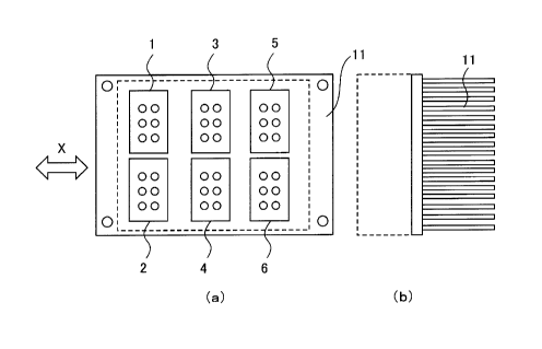
CA 02653207 2008-11-21
FIG. 2 is a layout configuration diagram showing a state
where the IGBT modules 1- 6 in FIG. 1 are disposed on the same
plane of a cooler 11. FIG. 2(a) is a view of the power converter
seen from the IGBT module mounting surface, while FIG. 2(b) is
a view seen from the side surface of the cooler.
As shown in FIG. 2, in the power converter of Embodiment
1, in the case where all the IGBT modules 1 -. 6 constituting
the positive-side and negative-side semiconductor switching
arms are disposed on the same plane of the cooler 11, the IGBT
modules 1 - 6 are arranged so that their longer latus sides may
become perpendicular to the direction X of a cooling wind (that
is, the traveling direction of a vehicle).
[0015]
In accordance with the power converter of Embodiment 1
as has such a layout configuration, the longer latus sides of
the IGBT modules 1 - 6 are located perpendicularly to the
direction (arrow X) of the cooling wind,--so that the area of
each of the IGBT modules 1 - 6 as receives the cooling wind can
be enlarged. In addition, since the direction from the windward
to the leeward is on the shorter latus sides of the IGBT modules,
a distance from the windward to the leeward can be shortened,
and the difference between the temperatures of the IGBT modules
on a windward side and a leeward side can be made small, whereby
it is permitted to efficiently cool the IGBT modules.
Accordingly, the heat radiation section of the cooler 11 can
11
CA 02653207 2008-11-21
be made small, reduction in the size of the cooler can be realized,
and the lowering of a cost is permitted in correspondence with
the smaller size of the cooler.
[0016]
Incidentally, FIG. 7 shows the layout configuration of
the IGBT modules 1 - 6 in the case where a cooler 20 of heatsink
type employing fins of grid type is used as the cooler. It is
needless to say that, even when such a cooler 20 is used, the
same advantages as stated above are achieved. That is, the
cooler may be any one which has a plurality of fins and in which
the longer latus sides of IGBT modules are located
perpendicularly to the direction of a cooling wind.
[0017]
EMBODIMENT 2:
FIGS. 3 and 4 show a power converter in Embodiment 2 of
this invention. FIG. 3 is a principal circuit configuration
d.iagram of -- the power converter, and- -FIG.- 4 is a layout
configuration diagram showing a state where semiconductor
element modules in FIG. 3 are disposed on a cooler. FIG. 4(a)
is a view of the power converter seen from a semiconductor
element module mounting surface, while FIG. 4 (b) is a view seen
from the side surface of the cooler.
Referring to FIGS. 3 and 4, numeral 12 designates the same
IGBT module as in Embodiment 1. The IGBT module forms the
positive-side semiconductor switching arm of the power
12
CA 02653207 2008-11-21
converter, and its collector terminal C is connected to the
anode terminal P of a DC power supply 10. Numeral 13 designates
a diode module (also termed "rectifying semiconductor element")
The diode module forms the negative-side semiconductor
rectification arm of the power converter, and its anode terminal
A is connected to the cathode terminal N of the DC power supply
10. The emitter terminal E of the IGBT module 12 and the cathode
terminal K of the diode module 13 are connected in series, and
an output terminal 14 is led out from the series joint of the
series connection.
[0018]
As shown in FIG. 4, the IGBT module 12 and the diode module
13 are arranged on the same plane of the cooler 15 so that their
longer latus sides may become perpendicular to the direction
of a cooling wind (that is, the traveling direction of a
vehicle).
That is, the -point of difference of Embodiment 2--from
Embodiment 1 is only the principal circuit configuration of the
power converter, and even with the principal circuit
configuration of such Embodiment 2, the same advantages as in
Embodiment 1 can be obtained by arranging the IGBT module 12
and the diode module 13 on the same plane of the cooler 15 so
that the longer latus sides thereof may become perpendicular
to the direction of the cooling wind.
[0019]
13
CA 02653207 2008-11-21
More specifically, the longer latus side of the IGBT
module 12 and the longer latus side of the diode module 13 are
located perpendicularly to the direction of the cooling wind,
so that those areas of the IGBT module 12 and the diode module
13 which receive the cooling wind can be enlarged. In addition,
since a direction from the windward to the leeward is on the
shorter latus sides of the IGBT module and the diode module,
a distance from the windward to the leeward can be shortened,
and it is permitted to efficiently cool the modules.
Accordingly, the heat radiation section of the cooler can be
made small, reduction in the size of the cooler can be realized,
and the lowering of a cost is permitted in correspondence with
the smaller size of the cooler.
[0020]
EMBODIMENT 3:
FIGS. 5 and 6 show a power converter in Embodiment 3 of
this invention. -FIG. 5-is a principal -circuit conf-iguration-
diagram of the power converter, and FIG. 6 is a layout
configuration diagram showing a state where semiconductor
element modules in FIG. 5 are disposed on a cooler. FIG. 6(a)
is a view of the power converter seen from a semiconductor
element module mounting surface, while FIG. 6(b) is a view seen
from the side surface of the cooler.
Referring to FIGS. 5 and 6, numeral 12 designates the same
IGBT module as in Embodiment 2. The IGBT module forms the
14
CA 02653207 2008-11-21
negative-side semiconductor switching arm of the power
converter, and its emitter terminal E is connected to the
cathode terminal N of a DC power supply 10. Numeral 13
designates a diode module (also termed "rectifying
semiconductor element"). The diode module forms the
positive-side semiconductor rectification arm of the power
converter, and its cathode terminal K is connected to the anode
terminal P of the.DC power supply 10. The collector terminal
C of the IGBT module 12 and the anode terminal A of the diode
module 13 are connected in series, and an output terminal 18
is led out from the series joint AC of the series connection.
[0021]
As shown in FIG. 6, the IGBT module 12 and the diode module
13 are arranged on the same plane of the cooler 19 so that their
longer latus sides may become perpendicular to the direction
of a cooling wind (that is, the traveling direction of a
vehicle) ;.
That is, the point of difference of Embodiment 3 from
Embodiment 2 is only the fact that the connection relationship
between the IGBT module 12 and the diode module 13 is a vertically
opposite relationship, in other words, that the diode module
13 has become the positive-side semiconductor rectification arm,
while the IGBT module 12 has become the negative-side
semiconductor switching arm. Even with such Embodiment 3,
quite the same advantages as in Embodiment 2 are obtained.
CA 02653207 2008-11-21
[0022]
EMBODIMENT 4:
Embodiment 4 of this invention will be described with
reference to FIGS.8-15. Incidentally, throughout the figures,
identical numerals and signs shall indicate identical or
corresponding parts.
The invention of Embodiment 4 relates to wiring
structures which are used in the power converter of Embodiment
1 stated above, and it has attained reduction in the wiring
inductances of circuits.
[0023]
FIG. 8 shows an arrayal diagram (FIG. 8(a)) of IGBT
modules on a positive side and a negative side and a diagram
(FIG. 8 (b) ) of wiring circuits based on flat conductors, in the
power converter of Embodiment 4.
Referring to FIG. 8, each of the IGBT modules 1 - 6 is
an IGBT module (also termed "switching semiconductor -element")
which has three collector terminals C and emitter terminals E.
As shown in FIG. 8(b), the IGBT modules 1, 3 and 5 form the
positive-side semiconductor switching arms of the power
converter, and the IGBT modules 2, 4 and 6 form the negative-side
semiconductor switching arms. As will be stated later, the IGBT
modules 1, 3 and 5 have the respective collector terminals C
connected to the anode terminal P of a filter capacitor 10
serving as a DC voltage supply, by one first flat bus bar (also
16
CA 02653207 2008-11-21
termed "first flat conductor") 24 which is common to all phases.
Likewise, the emitter terminals E of the IGBT modules 2, 4 and
6 are connected to the cathode terminal N of the filter capacitor
by one second flat bus bar (also termed "second flat
conductor") 25 which is common to all the phases.
[0024]
Besides, the emitter terminal E of the IGBT module 1 and
the collector terminal C of the IGBT module 2 are connected by
a third flat bus bar (also termed "third flat conductor") 21,
and the third flat bus bar 21 is connected to the AC output
terminal 7 of the U-phase. Besides, the emitter terminal E of
the IGBT module 3 and the collector terminal C of the IGBT module
4 are connected by a third flat bus bar 22, and the third flat
bus bar 22 is connected to the AC output terminal 8 of the V-phase.
Likewise, the emitter terminal E of the IGBT module 5 and the
collector terminal C of the IGBT module 6 are connected by a
third fla=t-bus bar 23, and the third flat bus bar 23 i-s-connected
to the AC output terminal 9 of the W-phase.
[0025]
FIG. 9 is a diagram showing the structures of the above
connections between the IGBT modules 1 - 6 and the third flat
bus bars 21, 22 and 23. The third flat bus bar 21 has the
structure in which it is connected to the three emitter
terminals E of the IGBT module 1 and the three collector
terminals C of the IGBT module 2, and in which it is provided
17
CA 02653207 2008-11-21
with openings and formed with spaces, so as not to touch the
parts of the collector terminals C of the IGBT module 1 and the
emitter terminals E of the IGBT module 2.
That is, the third flat bus bar 21 is disposed so as to
be connected with the output terminal 7 in a state where it
connects the E terminals of the IGBT module 1 and the C terminals
of the IGBT module 2, and where it strides over the C terminals
of the IGBT module 1 and the E terminals of the IGBT module 2
so as not to be connected with these C terminals and E terminals.
[0026]
Likewise, the third flat bus bar 22 has the structure in
which it is connected to the three emitter terminals E of the
IGBT module 3 and the three collector terminals C of the IGBT
module 4, and in which it is provided with openings and formed
with spaces, so as not to touch the parts of the collector
terminals C of the IGBT module 3 and the emitter terminals E
of-the IGBT mo-dule 4.
That is, the third flat bus bar 22 is disposed 'so as to
be connected with the output terminal 8 in a state where it
connects the E terminals of the IGBT module 3 and the C terminals
of the IGBT module 4, and where it strides over the C terminals
of the IGBT module 3 and the E terminals of the IGBT module 4
so as not to be connected with these C terminals and E terminals.
[0027]
Also the third flat bus bar 23 has the structure in which
18
CA 02653207 2008-11-21
it is connected to the three emitter terminals E of the IGBT
module 5 and the three collector terminals C of the IGBT module
6, and in which it is provided with openings and formed with
spaces, so as not to touch the parts of the collector terminals
C of the IGBT module 5 and the emitter terminals E of the IGBT
module 6.
That is, the third flat bus bar 23 is disposed so as to
be connected with the output terminal 8 in a state where it
connects the E terminals of the IGBT module 5 and the C terminals
of the IGBT module 6, and where it strides over the C terminals
of the IGBT module 5 and the E terminals of the IGBT module 6
so as not to be connected with these C terminals and E terminals.
[0028a
FIG. 10 is a wiring structure diagram of the first flat
bus bar 24 which connects the anode terminal P of the filter
capacitor 10 being the DC voltage supply and the respective
collector terminals C of the IGBT modules 1, 3 and 5 as shown
in FIG. 8 (b) .
As shown in FIG. 10, the first flat bus bar 24 is so
configured that the respectively three collector terminals C
of the IGBT modules 1, 3 and 5 are all connected in common and
then to the anode terminal P of the filter capacitor 10.
Besides, the first flat bus bar 24 is put into a structure
in which it is provided with openings and formed with spaces
so that the respective emitter terminals E of the IGBT modules
19
CA 02653207 2008-11-21
1, 3 and 5 and this bus bar may not come into touch.
[0029]
FIG. 11 is a diagram showing the wiring structure of the
second flat bus bar 25 which connects the cathode terminal N
of the filter capacitor 10 and the respective emitter terminals
E of the IGBT modules 2, 4 and 6 as shown in FIG. 8(b). The
second flat bus bar 25 is so configured that the respectively
three emitter terminals E of the IGBT modules 2, 4 and 6 are
all connected in common and then to the cathode terminal N of
the filter capacitor 10.
Besides, the second flat bus bar 25 is put into a structure
in which it is provided with openings and formed with spaces
so that the respective collector terminals C of the IGBT modules
2, 4 and 6 and this bus bar may not come into touch.
[0030]
Incidentally, regarding the arrangement relationship
among the third flat bus bar 21 (or 22 or 23), the first filat
bus bar 24 and the second flat bus bar 25 as stated above, these
bus bars are disposed so as to become parallel flat plates in
a stacked structure in which they are stacked one over another
as shown in FIG. 12.
The first - third flat conductors are connected to the
terminals of the IGBTs by, for example, screwing. In connecting
the flat conductors and the terminals, a measure such as bending
the flat conductor, providing a lug, or providing a collar is
CA 02653207 2008-11-21
taken if necessary. In the vicinity of the connection parts
of any flat conductor with the terminals of the IGBTs, another
flat conductor is provided with the openings as stated before,
so that the other flat conductor and the terminals may not be
connected. Although the flat conductors have been arranged at
intervals in FIG. 12, a structure in which the flat conductors
are stacked with insulating members interposed therebetween may
well be used. Besides, although the second flat conductor 25,
the first flat conductor 24 and the third flat conductors 21
- 23 have been arranged nearer to the IGBT modules 1- 6, the
arrangement order of the flat conductors may well be changed.
[0031]
Next, the action of the reduction of the principal circuit
wiring inductance featuring Embodiment 4 will be described in
conjunction with FIG. 13.
The magnitude of the principal circuit wiring inductance
is influenced by the- :length of a wiring line; and the magnitude-
of a magnetic field which is generated in conformity with the
corkscrew rule on the basis of the flow of a current. For the
purpose of making the principal circuit wiring inductance small,
accordingly, it is required (1) to shorten the wiring line
length, and (2) to make small the magnetic field which is
generated by the flow of the current.
[0032]
FIG. 13(a) illustrates the relationship between the
21
CA 02653207 2008-11-21
directions of currents and generated magnetic fields.
Referring to FIG. 13 (a) , in a case where a current Ii and
a current 12 are located so as to go and return, in a loop through
which a current I flows, the direction of a magnetic field (DI1
generated by the current 11 and the direction of a magnetic field
(DI2 generated by the current 12 fall into the opposite
relationship. Accordingly, an inductance decreases by
canceling the magnetic fields each other.
[0033]
FIG. 13 (c) is a diagram for explaining the current paths
of, for example, the U-phase. A current which is outputted from
the anode terminal P of the filter capacitor 10, flows via the
P terminal --> the first flat bus bar 24 --> a current Il ---> the
C terminal of the positive-side arm IGBT module 1-~ the E
terminal thereof --> the third flat bus bar 21 --> a current 12
--> the U terminal. Besides, a current which returns from the
U terminal flows via th-e- U terminal --~ the -third flat 'bus bar
21 -> a current 13 ~ the C terminal of the IGBT module 2 of
the negative-side arm --> the E terminal thereof -> a current
14 ---> the second flat bus bar 25 -> the cathode terminal N of
the filter capacitor 10.
[0034]
FIG. 13 (b) illustrates the states of the connection paths
of the flat bus bars 21, 24 and 25 shown in FIGS. 9 - 11, and
shows the current paths of the above currents 11, 12, 13 and
22
CA 02653207 2008-11-21
14.
As seen from FIG. 13 (b) , the currents Ii and 12 and the
currents 13 and 14 flow so as to go and return, respectively.
That is, the currents to flow can be caused to go and return,
by configuring the flat bus bars as shown in FIGS. 9- 11, whereby
the inductances of the wiring lines can be reduced as explained
in conjunction with FIG. 13(a).
[0035]
Further, the comparisons of wiring inductances between
the power converter in Embodiment 4 of this invention and a
prior-art apparatus will be described with reference to FIGS.
14 and 15.
FIG. 14 illustrates wiring paths and the inductances of
wiring lines in the prior-art apparatus. The prior-art
apparatus is so configured that a filter capacitor 10 and a
U-phase, the filter capacitor 10 and a V-phase, and the filter
capacitor 10 and a W-phase are respectively connected in -a
manner to be divided for the individual phases. Therefore,
inductances Lp exist in the respective wiring lines from the
P (positive side) terminal of the filter capacitor 10 to the
C terminal of the IGBT of a U-phase upper (positive side) arm,
from the P terminal of the filter capacitor 10 to the C terminal
of the IGBT of a V-phase upper arm, and from the P terminal of
the filter capacitor 10 to the C terminal of the IGBT of a W-phase
upper arm.
23
CA 02653207 2008-11-21
Besides, inductances Ln exist in the respective wiring
lines from the N (negative side) terminal of the filter
capacitor 10 to the E terminal of the IGBT of a U-phase lower
(negative side) arm, from the N terminal of the filter capacitor
to the E terminal of the IGBT of a V-phase lower arm, and
from the N terminal of the filter capacitor 10 to the E terminal
of the IGBT of a W-phase lower arm.
On this occasion, a switching surge voltage which is
generated at the switching of each IGBT is expressed by the
relationship of (Lp + Ln) x (switching di/dt of the IGBT).
[0036]
On the other hand, the state of the wiring lines in
Embodiment 4 is such that, as shown in FIG. 15, the C terminals
of the IGBT modules of the respective upper (positive side) arms
of the U-phase, V-phase and W-phase are collectively connected
from the P (positive side) terminal of the filter capacitor 10,
while-t-he E-terminals of the IGBT modules of the respective lower
(negative side) arms of the U-phase, V-phase and W-phase are
collectively connected from the N (negative side) terminal of
the filter capacitor 10. Therefore, the inductances of the
wiring lines from the P terminal of the filter capacitor to the
C terminals of the IGBT modules of the upper arms become a form
in which the wiring inductances of the U-phase, V-phase and
W-phase are connected in parallel, and these inductances become
1/3 of the inductances Lp of the prior-art example in FIG. 14.
24
CA 02653207 2008-11-21
Likewise, the inductances of the wiring lines between the N-side
terminal of the filter capacitor and the respective phases U,
V and W become 1/3 of the inductances Ln in the prior-art example.
j0037]
As stated above, in accordance with the power converter
in Embodiment 4 of this invention, the inductances of the wiring
lines can be made small, a snubber circuit which suppresses the
switching surge voltage of the IGBT and which is usually
required is dispensed with, the number of components is
decreased, and not only the reduction of the size of the
apparatus, but also the lowering of the cost thereof can be
attained.
[0038]
EMBODIMENT 5:
Embodiment 5 of this invention is shown in FIG. 16. The
invention of Embodiment 5 relates to wiring structures which
are-used in the power converter of Embodiment 2- stated- above,
and it has attained reduction in the wiring inductances of
circuits.
FIG. 16(a) is a diagram showing the arrayals and wiring
structures of the positive-side and negative-side
semiconductor elements in the power converter, and FIG. 16 (b)
shows a diagram of a wiring circuit based on flat bus bars.
Referring to FIG. 16, numeral 12 designates the IGBT
module which has three collector terminals C and emitter
CA 02653207 2008-11-21
terminals E, which forms the positive-side semiconductor
switching arm of the power converter, and the collector
terminals C of which are connected to the anode terminal P of
the DC power supply 10.
Numeral 13 designates the diode module (also termed
"rectifying semiconductor elements") which has anode terminals
A and cathode terminals K, which forms the negative-side
semiconductor rectification arm of the power converter, and the
anode terminals A of which are connected to the cathode terminal
N of the DC power supply 10. The emitter terminals E of the
IGBT module 12 and the cathode terminals K of the diode module
13 are connected in series, and the output terminal 14 is led
out from the series joint of the series connection.
Incidentally, FIG. 16 shows the configuration of an
output arm corresponding to one phase of the power converter,
and it is needless to say that, in case of a three-phase power
converter-by way-of example, three output-arms are connected
between the positive and negative terminals of the DC power
supply 10.
[0039)
Here, in the same manner as in Embodiment 4 stated before,
the IGBT module 12 has the collector terminals C connected to
the anode terminal P of the DC power supply 10 by one first flat
bus bar (also termed "first flat conductor") 28, and the anode
terminals A of the diode module 13 are connected to the cathode
26
CA 02653207 2008-11-21
terminal N of the DC power supply 10 by one second flat bus bar
(also termed "second flat conductor") 29.
Besides, the emitter terminals E of the IGBT module 12
and the cathode terminals K of the diode module 13 are connected
by a third flat bus bar (also termed "third flat conductor")
26, and the third flat bus bar 26 is connected to the output
terminal 14.
[0040]
As shown in FIG. 16 (a) , the third flat bus bar 26 has a
structure in which it is connected to the three emitter
terminals E of the IGBT module 12 and the two cathode terminals
K of the diode module 13, and in which it is provided with
openings and formed with spaces so as not to touch the parts
of the collector terminals C of the IGBT module 12 and the anode
terminals A of the diode module 13.
In other words, the third flat bus bar 26 is disposed so
as to b-e connected with the output terminal-14 in a stat,e-where
it connects the E terminals of the IGBT module 12 and the cathode
terminals K of the diode module 13, and where it strides over
the C terminals of the IGBT module 12 and the anode terminals
A of the diode module 13 so as not to be connected with these
C terminals and A terminals.
[0041]
That is, the point of difference of Embodiment 5 from
Embodiment 4 is only the fact that the principal circuit
27
CA 02653207 2008-11-21
configuration of the power converter is different. Even with
such a principal circuit configuration of Embodiment 5, the same
advantages as in Embodiment 4 can be obtained by forming the
wiring structures based on the flat conductors, similar to those
in Embodiment 4, as stated above.
[0042]
EMBODIMENT 6:
FIG. 17 shows Embodiment 6 of this invention, and FIG.
17 (a) is a diagram showing the arrayals and wiring structures
of positive-side and negative-side semiconductor elements in
a power converter, while FIG. 17 (b) shows a diagram of a wiring
circuit based on flat bus bars.
The invention of Embodiment 6 relates to the wiring
structures which are used in the power converter of Embodiment
3 stated above. The point of difference of Embodiment 6 from
Embodiment 5 is only the fact that the connection relationship
--between the IGBT module 12 and the diode module 13 is a vertically
(positive and negative signs) opposite relationship, in other
words, that the diode module 13 has become the positive-side
semiconductor rectification arm, while the IGBT module 12 has
become the negative-side semiconductor switching arm. The
remaining configuration is quite the same as in Embodiment S.
[0043]
That is, the cathode terminals K of the diode module 13
are connected to the anode terminal P of the DC power supply
28
CA 02653207 2008-11-21
by one first flat bus bar 28, and the emitter terminals E
of the IGBT module 12 are connected to the cathode terminal N
of the DC power supply 10 by one second flat bus bar 29.
Besides, the anode terminals A of the diode module 13 and
the collector terminals C of the IGBT module 12 is connected
by a third flat bus bar 27, and the third flat bus bar 27 is
connected to the output terminal 18.
[0044]
As shown in FIG. 17(a), the third flat bus bar 27 has a
structure in which it is connected to the two anode terminals
A of the diode module 13 and the three collector terminals C
of the IGBT module 12, and in which it is provided with openings
and formed with spaces so as not to touch the parts of the cathode
terminals K of the diode module 13 and the emitter terminals
E of the IGBT module 12.
[0045]
-- Even with such-a principal circuit conf-iguration of
Embodiment 6, the same advantages as in Embodiment 4 can be
obtained by forming the wiring structures based on the flat
conductors, similar to those in Embodiment 4.
INDUSTRIAL APPLICABILITY
[0046]
This invention is applicable to power converters which
are mounted on the vehicles of a railway, etc.
29