Note: Descriptions are shown in the official language in which they were submitted.
CA 02653315 2009-02-09
SOLDERABLE ELASTIC ELECTRIC CONTACT TERMINAL
BACKGROUND ART
Field of the Invention
[0001] The present invention relates to an electric contact terminal, and
particularly, to an elastic electric contact terminal adapted to perform a
soldering process
on the elastic electric contact terminal while electrically and mechanically
connecting an
object to a printed circuit board. More particularly, the present invention
relates to an
elastic electric contact terminal adapted to perform a reflow soldering
process with a
surface mounting process on the elastic electric contact terminal.
Description of the Related Art
[0002] Generally, solderable elastic electric contact terminals must have high
electrical conductivity and excellent elastic resilience and must be resistant
to a soldering
temperature.
[0003] Related art reflow-solderable electric contact terminals are formed
mainly
of metal. Specifically, beryllium copper is widely used for the electric
contact terminals
because it has excellent elastic resilience and high electrical conductivity.
For example, a
beryllium copper sheet, having a thickness of about 0.3 mm or less and a
predetermined
width, is blanked with a press mold to have a predetermined shape, and then is
heat-
treated to form the electric contact terminal having an improved elastic
resilience.
[0004] However, the electric contact terminals formed of only the metal sheet,
because of metal characteristics or structures, cannot provide excellent
elasticity in a
predetermined height or less. To increase the elasticity, the metal sheet must
be bent in a
predetermined shape to have a bent height that mainly determines the height of
the
1
CA 02653315 2009-02-09
electric contact terminal, so that the electric contact terminal cannot
provide elasticity in a
predetermined height or less. In addition, since a single press mold can form
products
having an identical shape, additional expensive press molds are needed to form
products
having different shapes. Furthermore, the light-weight electric contact
terminal formed
of a metal sheet can be moved by the wind supplied in a surface mounting
process,
thereby causing defect.
[00051 Another related art is disclosed in EP Patent EP 1090538 issued to Gore
Enterprise Holdings Inc (US). According to this patent, an additional adhesive
is needed
to fix an electrically conductive gasket material and a solderable support
layer, thereby
causing inconvenience. Furthermore, the adhesive increases electric
resistance.
[0006) Further another related art is disclosed in U.S Patent No. 7,129,421
issued
to the Gore Enterprise Holdings Inc (US). According to this patent, a
compression hole
is provided to an electrically conductive gasket material, and an electrically
conductive
support layer, that goes through a crimp process, is provided to a bottom
surface of the
electrically conductive gasket material, thereby reducing the productivity of
electromagnetic interference (EMI) gasket assemblies. That is, after the
electrically
conductive gasket material is manufactured, the electrically conductive
support layer, that
is separately manufactured, is inserted into the compression hole of the
electrically
conductive gasket material and then pressed, thereby causing inconvenience.
The
compression hole has a smaller size than the EMI gasket assembly. Hence, a
size of the
electrically conductive support layer in the compression hole is limited
thereby, so that an
adhesive force is not sufficient between the electrically conductive gasket
material and
the electrically conductive support layer. That is, when the EMI gasket
assembly is
drawn in an upper direction, the electrically conductive gasket material is
easily removed
from the electrically conductive support layer.
2
CA 02653315 2009-02-09
Summary of the Invention
[0007] An object of the present invention is to provide an elastic electric
contact
terminal having good elasticity and good electrical conductivity.
[0008] Another object of the present invention is to provide a solderable
elastic
electric contact terminal.
[0009] A further another object of the present invention is to provide an
elastic
electric contact terminal having low manufacturing costs and improved
production
efficiency.
[0010] A still further another object of the present invention is to provide
an
elastic electric contact terminal that is adapted for a surface-mounting
process with a
vacuum pick-up process, and a reflow-soldering process.
[0011] An even further another object of the present invention is to provide
an
elastic electric contact terminal that receives leakage of an insulating non-
foam rubber
coating layer to prevent the leakage from interfering in a soldering
operation.
[0012] A yet further another object of the present invention is to provide an
elastic electric contact terminal having similar lateral soldering strengths
after a soldering
process.
[0013] A yet further another object of the present invention is to provide an
elastic electric contact terminal having upper and lower surfaces that are
easily
distinguished from each other without an additional distinguishing mark.
[0014] A yet further another object of the present invention is to provide an
elastic electric contact terminal that can improve solder-rising phenomenon at
both side
surfaces thereof to have a reliable soldering strength.
[0015] A yet further another object of the present invention is to provide an
3
CA 02653315 2009-02-09
elastic electric contact terminal that can achieve the arrangement of upper
and lower
surfaces through vibration in a reel packaging process and reduce movement of
the
electric contact terminal in a reflow soldering process, by disposing the
center of gravity
of the electric contact terminal in a lower part.
[0016] A yet further another object of the present invention is to provide an
elastic electric contact terminal that limits the maximum range where the
electric contact
terminal can be pressed.
[0017] A yet further another object of the present invention is to provide an
elastic electric contact terminal that can reliably maintain a top thereof in
a plane.
[0018] According to an aspect of the present invention, there is provided a
solderable elastic electric contact terminal including: a tube-shaped
insulating elastic
core; an insulating non-foam rubber coating layer adhered to the insulating
elastic core to
surround the insulating elastic core; and a heat-resistant polymer film having
one surface
adhered to the insulating non-foam rubber coating layer to surround the
insulating non-
foam rubber coating layer, and another surface integrally provided with a
metal layer.
[0019] According to another aspect of the present invention, there is provided
a
solderable elastic electric contact terminal including: a tube-shaped
insulating elastic core
including a through hole in an inner portion thereof, an insulating non-foam
rubber
coating layer adhered to the insulating elastic core to surround the
insulating elastic core;
and a heat-resistant polymer film having one surface adhered to the insulating
non-foam
rubber coating layer to surround the insulating non-foam rubber coating layer,
and
another surface integrally provided with a metal layer; wherein the heat-
resistant polymer
film is adhered to the insulating non-foam rubber coating layer such that both
ends of the
heat-resistant polymer film are spaced apart from each other, and when the
heat-resistant
polymer film is adhered to the insulating non-foam rubber coating layer, a
leakage of the
4
CA 02653315 2009-02-09
insulating non-foam rubber coating layer sticking out of the both ends of the
heat-
resistant polymer film is received in a receiving space defined by the spaced
both ends of
the heat-resistant polymer film.
[00201 According to a further another aspect of the present invention, there
is
provided a solderable elastic electric contact terminal including: a tube-
shaped insulating
elastic core; a metal reinforcement on a bottom of the insulating elastic
core; an
insulating non-foam rubber coating layer adhered to both the metal
reinforcement and the
insulating elastic core to surround both the metal reinforcement and the
insulating elastic
core; and a heat-resistant polymer film having one surface adhered to the
insulating non-
foam rubber coating layer to surround the insulating non-foam rubber coating
layer, and
another surface integrally provided with a metal layer; wherein both ends of
the heat-
resistant polymer film is spaced a predetermined distance from each other.
[00211 According to a still further another aspect of the present invention,
there
is provided a solderable elastic electric contact terminal including: a tube-
shaped
insulating elastic core; an insulating non-foam rubber coating layer adhered
to the
insulating elastic core to surround the insulating elastic core; and a heat-
resistant polymer
film having one surface adhered to the insulating non-foam rubber coating
layer to
surround the insulating non-foam rubber coating layer, and another surface
integrally
provided with a metal layer, wherein a heat-resistant double-sided adhesive
tape is
attached to a portion of a bottom of the metal layer, and the heat-resistant
double-sided
adhesive tape is directly adhered to a printed circuit board.
Brief Description of the Drawings
[00221 The above objects and other advantages of the present invention will
become
more apparent by describing in detail preferred embodiments thereof with
reference to the
5
CA 02653315 2009-02-09
attached drawings in which:
[0023] FIG. 1 is a view of an electric contact terminal according to an
embodiment
of the present invention;
[0024] FIG. 2 is a view of an electric contact terminal according to another
embodiment of the present invention;
[0025] FIG. 3 is a view of an electric contact terminal according to a further
another
embodiment of the present invention;
[0026) FIG. 4 is a view of an electric contact terminal according to a still
further
another embodiment of the present invention;
[0027] FIG. 5 is a view of an electric contact terminal according to an even
further
another embodiment of the present invention;
[0028] FIG. 6 is a view of an electric contact terminal according to a yet
further
another embodiment of the present invention;
[0029] FIG. 7 is a view illustrating an application of the electric contact
terminal in
FIG. 6 according to an embodiment of the present invention; and
[0030] FIG. 8 is a view illustrating the electric contact terminal that is
surface-
mounted to a printed circuit board according to an embodiment of the present
invention.
Detailed Description of the preferred Embodiments
[0031] Now, preferred embodiments of the present invention will be described
in
detail with reference to the accompanying drawings.
[0032] 1. ONE EMBODIMENT
[0033] FIG. I is a view of an electric contact terminal 100 according to one
embodiment of the present invention.
[0034] Referring to FIG. 1, the elastic electric contact terminal 100 includes
a
6
CA 02653315 2011-05-31
tube-shaped insulating elastic core 10, an insulating non-foam rubber coating
layer 20,
and a heat-resistant polymer film 30 having a metal layer 40 provided to a
surface thereof,
which are sequentially stacked.
[00351 In this structure, the tube-shaped elastic core manufactured through an
extrusion process is applied, thereby reducing manufacturing costs, adjusting
an elastic
force and a pressing force to control the size of a through hole of the tube,
and efficiently
manufacturing a small product. Also, the insulating non-foam rubber coating
layer
maintains an adhesive force and an elastic force before and after a soldering
process and
during a repeated compression test. Also, the heat-resistant polymer film
including the
metal layer meets a soldering condition and improves flexibility and maintains
an elastic
force during a compression test, and the metal layer is adapted for a
soldering process
using a solder cream.
100361 1.1 INSULATING ELASTIC CORE 10
[00371 Referring to FIG. 1, the insulating elastic core 10 is disposed at the
most
inner part and has a tube shape, which has a tetragonal cross-section in this
embodiment.
However, the cross-section of the insulating elastic core 10 is not limited
thereto, and
may vary according to an extrusion process. For example, in the cross-section
of the
insulating elastic core 10, the thickness of both sidewalls may be less than
that of top and
bottom walls to improve flexibility and reduce a pressing force.
[00381 The insulating elastic core 10 may be formed of a non-foam heat-
resistant
elastic rubber, e.g., a silicon rubber to meet reflow soldering and elasticity
conditions.
[00391 Also, the hardness of the insulating elastic core 10 may range from
Shore
A 40 to 70 for appropriate mechanical strength and elasticity.
[0040) Also, both edges of a top of the insulating elastic core 10 may be
rounded.
This structure is easy to handle and prevents the catch on both sides in the
process where
7
CA 02653315 2009-02-09
the completed electric contact terminal 100 is attached to a printed circuit
board through a
soldering process and then coupled to a facing object.
[00411 Also, the insulating elastic core 10 may have a different color from
that of
the metal layer 40.
[00421 1.2 INSULATING NON-FOAM RUBBER COATING LAYER 20
[00431 The insulating non-foam rubber coating layer 20 is disposed between the
insulating elastic core 10 and the heat-resistant polymer film 30 to reliably
adhere the
insulating elastic core 10 to the heat-resistant polymer film 30. Furthermore,
the
insulating non-foam rubber coating layer 20 is required to maintain the
adhesive force
before and after the soldering process, and maintain elasticity at all times.
For example,
for flexibility and elasticity, when the insulating non-foam rubber coating
layer 20 is
completely hardened, the hardness of the insulating non-foam rubber coating
layer 20
may range from Shore A 20 to 60, and the thickness thereof may range from
about 0.02
mm to 0.2 mm.
[00441 The insulating non-foam rubber coating layer 20 may be formed by
hardening a liquid silicon rubber that is the selected one of a silicon rubber
hardened by
heat and a silicon rubber hardened by moisture. For example, to increase
working speed,
the rubber completely hardened by heat may be used.
100451 The liquid silicon rubber is adhered to a facing object during
hardening,
and the insulating non-foam rubber coating layer 20 is in a solid state after
the hardening.
The hardened insulating non-foam rubber coating layer 20 maintains the
elasticity and the
adhesive force against reheating. For example, to obtain a reliable adhesive
force, an
adhesion enhancer is added to a liquid silicon rubber, or a surface-treating
process
including corona treating is performed on an object for adhesion, that is, the
elastic core
10 or the heat-resistant polymer film 30.
8
CA 02653315 2011-05-31
[0046] For example, a piezoelectric powder or a magnetic powder such as
ferrite
may be mixed with a liquid silicon rubber and hardened such that the
insulating non-foam
rubber coating layer 20 have magnetic or piezoelectric characteristics. In
this case, the
noise of current flowing through the metal layer 40 can be removed.
[0047] 1.3 HEAT-RESISTANT POLYMER FILM 30
[0048] The heat-resistant polymer film 30 may be, e.g., one of a polyimide
(PI)
film having good heat resistance and other heat-resistant polymer films, and
have a
thickness, e.g., ranging from about 0.01 mm to 0.05 mm considering flexibility
and
mechanical strength.
[0049] Also, the metal layer 40 is integrally formed with an outer surface of
the
heat-resistant polymer film 30. In here, a predetermined portion of the metal
layer 40 is
removed using an etching process to improve the flexibility of the heat-
resistant polymer
film 30, or the metal layer 40 is divided into an electrically insulated
plurality of portions
using an etching process, and a ground pattern, to which an elastic electric
contact
terminal is soldered, is divided into a plurality of patterns having an
insulating gap to
correspond to each of a plurality of portions, so that the single electric
contact terminal
100 may be used as a plurality of electric contact terminals.
[0050] For example, the metal layer 40 may include a plurality of metal
layers,
and the metal layer 40 may be formed by sputtering metal on the heat-resistant
polymer
film 30, and then by plating the heat-resistant polymer film 30 with metal.
For example,
one layer of the metal layer 40 may be formed using a copper-plating process,
and a main
component of the entire metal layer 40 may be copper. The most outer surface
of the
metal layer 40 includes any one of tin, silver, and gold to prevent corrosion
and improve
a soldering process using a solder cream. For example, for the metal layer 40
to have a
strong soldering strength, a good electric transmittance, and a strong
adhesive force to a
9
CA 02653315 2011-05-31
heat-resistant polymer film, metal is coated on the heat-resistant polymer
film using a
sputtering process, then the copper-plating process is performed on the heat-
resistant
polymer film, and then a tin-plating process is performed on the heat-
resistant polymer
film. The metal layer 40 may have a thickness, e.g., ranging from about 0.002
mm to
0.01 mm considering flexibility or soldering characteristics and soldering
strength.
[00511 Meanwhile, the heat-resistant polymer film 30 provided with the metal
layer 40, e.g., may be a single-sided flexible copper clad laminate (FCCL).
[00521 1.4 METHOD OF MANUFACTURING ELECTRIC CONTACT
TERMINAL 100
[00531 Hereinafter, a method of manufacturing the electric contact terminal
100
will now be described.
[00541 A liquid silicon rubber hardened by heat is cast, using a casting
machine,
into a liquid silicon rubber coating layer having a thickness ranging from
about 0.02 mm
to 0.2 mm on an insulated surface of the heat-resistant polymer film 30 having
a constant
width and including the metal layer 40 on the outer surface thereof.
Meanwhile, the
elastic core 10, manufactured in a roll shape using an extrusion process, is
placed on the
liquid silicon rubber coating layer and surrounded through a jig having a
predetermined
shape.
[00551 At this point, when the liquid silicon rubber coating layer is too
thin, the
adhesive force between the insulating elastic core 10 and the heat-resistant
polymer film
is decreased, and when the coating layer is too thick, it takes a lot of time
to harden
the liquid silicon rubber. When the coating layer is formed of a liquid
silicon rubber
hardened by moisture, a coating process may be performed in a nitrogen or
vacuum
atmosphere.
25 [0056] Thereafter, the heat-resistant polymer film 30 surrounding the
insulating
CA 02653315 2011-05-31
elastic core 10 is located at a mold having similar dimensions to those of the
insulating
elastic core 10, and the liquid silicon rubber coating layer is hardened by
heat, disposed
between the insulating elastic core 10 and the heat-resistant polymer film 30.
Then, the
liquid silicon rubber coating layer is hardened and changed into the
insulating non-foam
rubber coating layer 20. At this point, the insulating non-foam rubber coating
layer 20
adheres the elastic core 10 and the heat-resistant polymer film 30 to each
other. That is,
the liquid silicon rubber coating layer is hardened by heat in outer space and
inner space
of the high-temperature mold having the constant dimensions, and then the
coating layer
becomes the insulating non-foam rubber coating layer 20 having elasticity
while serving
as an adhesive for attaching the insulating elastic core 10 and the heat-
resistant polymer
film 30.
100571 Since the hardened liquid silicon rubber is not melted again by heat,
even
when a soldering process is performed on the electric contact terminal 100,
the silicon
rubber maintains its original adhesive performance. At this point, to increase
a hardening
speed of the liquid silicon rubber located in the mold, a temperature of the
mold is
maintained at about 180 C, and an ambient humidity is maintained at about 60
%.
[00581 In addition, since the electric contact terminal 100 is manufactured
with
the heat-resistant polymer film 30 having the outer surface provided with the
metal layer
40, a long product is susceptible to wrinkling. Thus, the electric contact
terminal 100 is
generally manufactured with a length of about 1 in or less, and finally, cut
to have a
desired length of about 3 mm to 30 mm. Also, when a liquid silicon rubber,
hardened by
both moisture and heat, is used, a hardening time can be reduced.
100591 An outer surface of the electric contact terminal 100 manufactured
according to the above method is formed of the metal layer 40 to have a good
electrical
conductivity of about 0.01 0 or less, favorable soldering characteristics, and
improved
11
CA 02653315 2011-05-31
soldering strength. In this embodiment, the metal layer 40 is formed through
sputtering
and electroplating processes, and the main component of the metal layer 40 is
copper
plated with tin, and polyimide (PI) is used as the heat-resistant polymer film
30, and since
a silicon rubber is used as the insulating elastic core 10 and the insulating
non-foam
rubber coating layer 20, their original performance is maintained before and
after the
soldering process. Also, before and after the soldering process, the
electrical
conductivity and elastic resilience are excellent.
[00601 For example, a bottom of the heat-resistant polymer film 30 may have a
structure for improving a soldering operation with a printed circuit board,
and a top may
be partially horizontal such that a reflow soldering process can be performed
through a
surface-mounting process with a vacuum pick-up process.
[00611 2. ANOTHER EMBODIMENT
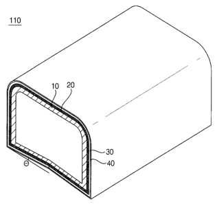
[00621 FIG. 2 is a view of an electric contact terminal 110 according to
another
embodiment of the present invention.
[00631 Referring to FIG. 2, a bottom of an insulating elastic core 10 may be
slantly formed in a width direction from both ends toward a middle portion in
a scoop
shape. A slant angle 8 may vary according to a physical property (e.g., the
coefficient
of thermal expansion) and dimensions of a silicon rubber. For example, the
slant angle
8 may range from about 1 to 10 .
[00641 In this structure, since the bottom of the insulating elastic core 10
has the
scoop shape from the both ends toward the middle portion, when being surface-
mounted
to a printed circuit board, a solder cream applied on a ground pattern fills
the scoop shape,
so that the both ends of the bottom of the insulating elastic core 10 does not
come off but
is reliably installed with the solder cream. Accordingly, solder-rising
phenomenon is
increased at both side surfaces of a metal layer 40 to further improve a
soldering strength
12
CA 02653315 2009-02-09
and prevent coming off phenomenon in one direction.
[0065] 3. FURTHER ANOTHER EMBODIMENT
[0066] FIG. 3 is a view of an electric contact terminal 120 according to a
further
another embodiment of the present invention.
[0067] Referring to FIG. 3, both ends of a heat-resistant polymer film 30 are
spaced a predetermined distance from each other to form a receiving space 32,
and
adhered to an insulating non-foam rubber coating layer 20. In this structure,
when the
heat-resistant polymer film 30 provided with the liquid insulating non-foam
rubber
coating layer 20 is passed through a mold (not shown) and compressed to
achieve
adhesion through heat hardening, an outside pressure due to the mold causes
the liquid
insulating non-foam rubber coating layer 20 to stick out of the both ends of
the heat-
resistant polymer film 30 to generate a leakage 21 that is received in the
receiving space
32 formed by the spaced both ends of the heat-resistant polymer film 30.
[0068] Thus, after the hardening, the solid leakage 21 of the insulating non-
foam
rubber coating layer 20, sticking out on an outer side of a metal layer 40
does not
interfere in a soldering operation for the metal layer 40. Also, in the state
where the
leakage 21 on which the soldering operation is not performed is received in
the receiving
space 32, when the soldering process is performed on the electric contact
terminal 120 on
a PCB, coming off phenomenon is prevented, and a soldering strength is
increased.
[0069] For example, the receiving space 32 may be bilaterally symmetrical
about
a center of a bottom of an insulating elastic core 10 to provide similar
soldering strengths
to lateral surfaces of the electric contact terminal 120 after a reflow
soldering process.
Also, the receiving space 32 distinguishes a top of the electric contact
terminal 120 from
the bottom. For example, the width of the receiving space 32 may depend on the
width
of the electric contact terminal 120 and be about 0.1 mm or more. Also, the
polymer film
13
CA 02653315 2011-05-31
30 having the expensive metal layer 40 is not attached to the receiving space
32, thereby
reducing costs.
[0070] In addition, since a solder cream is soldered to only the metal layer
40, the
solder cream disposed in the receiving space 32 moves toward both side
surfaces of the
metal layer 40 during the soldering operation, thereby increasing the
soldering strength.
[0071] Specifically, such as the embodiment of FIG. 2, when the bottom of the
insulating elastic core 10 is slantly formed in a scoop shape from both ends
toward a
middle portion in a width direction to define the receiving space 32, a space
for receiving
the leakage 21 of the insulating non-foam rubber coating layer 20 can be
further
substantially increased.
[0072] Also, in this structure, the receiving space 32 clearly distinguishes
the top
of the electric contact terminal 120 from the bottom thereof, thereby
achieving
convenient reel packaging with a vacuum pick-up process.
[0073] 4. STILL FURTHER ANOTHER EMBODIMENT
[0074] FIG. 4 is a view of an electric contact terminal 130 according to a
still further
another embodiment of the present invention.
[0075] Referring to FIG. 4, a metal reinforcement 50 is disposed at a bottom
of
an elastic core 10, and then an assembly including the elastic core 10 and the
metal
reinforcement 50 is enclosed with a heat-resistant polymer film 30 including a
metal
layer 40 on an outer surface thereof while interposing an insulating non-foam
rubber
coating layer 20 between the assembly and the heat-resistant polymer film 30.
At this
point, both ends of the heat-resistant polymer film 30 are spaced from each
other to form
a gap 34.
[0076] According to this embodiment, when the electric contact terminal 130 is
surface-mounted to a PCB, a solder cream is in contact with the metal
reinforcement 50
14
CA 02653315 2009-02-09
through the gap 34 to increase an adhesive force after a soldering process.
Also, the gap
34 easily distinguishes an upper part of the electric contact terminal 130
from a lower
part thereof, and in the case of a light-weight product, the self weight of
the metal
reinforcement 50 prevents the movement of the product due to wind supplied in
a surface
mounting process with a vacuum pick-up process.
[00771 5. EVEN FURTHER ANOTHER EMBODIMENT
[00781 FIG. 5 is a view of an electric contact terminal 140 according to an
even
further another embodiment of the present invention.
[00791 An insulating elastic core 10, having a tube shape, includes a through
hole
15 in an inner portion thereof. A cross-section of the elastic core 10 may be
circular or
tetragonal, but not limited thereto. Various shapes of the cross section are
provided
according to extrusion processes.
[00801 As described above, the hardness of the insulating elastic core 10 may
range Shore A 40 to 70 for appropriate mechanical strength and elasticity, and
a pressing
force for a top of the insulating elastic core 10 is determined according to a
size and a
shape of the through hole 15 disposed in the inner portion.
[00811 The through hole 15 in the inner portion of the elastic core 10 may be
disposed in an upper part of the insulating elastic core 10 such that the
center of gravity
of the insulating elastic core 10 is disposed in a lower part. That is,
referring to FIG. 5, a
lower portion 11 of the insulating elastic core 10 has a larger thickness than
other
portions 12 and 13, so that the through hole 15 is disposed in the upper part.
In this
structure, the center of the gravity of the insulating elastic core 10 is
disposed in the
lower part, thereby achieving the arrangement of upper and lower surfaces
through
vibration in a reel packaging operation, and reducing movement in a reflow
soldering
operation. In addition, the lower portion 11 of the insulating elastic core 10
is thick to
CA 02653315 2011-05-31
increase a self weight thereof and limit a pressing extent of an outside
pressure, thereby
placing the upper portion 12 in as nearly a horizontal position as possible
when
contacting a facing object. For example, in the thickness of the insulating
elastic core 10,
the lower portion 11 is thickest, and the both side portions 13 are thinnest
to reduce the
pressing force and keep the upper portion 12 in equilibrium.
[0082] The through hole 15 passing through the insulating elastic core 10 may
be
tetragonal, polygonal, circular, or oval.
[0083] In the case where the through hole 15 is tetragonal, the both side
portions
13 with respect to the through hole 15 decreases in width in an upper
direction, which are
symmetrical and slanted, and an outer surface of the insulating elastic core
10 may also
be slanted, corresponding to the both side portions 13. In this structure,
pressure applied
by an object contacting the top of the insulating elastic core 10 is dispersed
outside of
both side surfaces of the insulating elastic core 10 to prevent slanting of an
upper part of
the insulating elastic core 10 including the through hole 15.
[0084] Also, the upper portion 12 and the lower portion 11 have slanted middle
portions to form an upper protrusion 16 and a lower protrusion 17,
respectively. In this
structure, the upper portion 12 of the insulating elastic core 10 is
reinforced with the
upper protrusion 16 to prevent a center of the upper portion 12 from being
collapsed by
pressure applied to the top and maintain a plane. Also, the lower protrusion
17
concentrates weight in the lower portion 11 of the insulating elastic core 10
and limits a
deformation height of the through hole 15 by contacting the upper protrusion
16.
[0085] For example, the thickness of the both side portions 13 of the
insulating
elastic core 10 with respect to the through hole 15 may be less than those of
the lower and
upper portions 11 and 12 to improve press elasticity from the upper part.
[0086] 6. YET FURTHER ANOTHER EMBODIMENT
16
CA 02653315 2009-02-09
[00871 FIG. 6 is a view of an electric contact terminal according to a yet
further
another embodiment of the present invention. FIG. 7 is a view illustrating an
application of
the electric contact terminal of FIG. 6 according to an embodiment.
[00881 Referring to FIG. 6, a receiving groove 24 is longitudinally disposed
in a
bottom of an insulating elastic core 10 between both ends of a heat-resistant
polymer film
30. The receiving groove 24, together with the receiving space 32, receives
the greater
amount of leakage of the insulating non-foam rubber coating layer 20 to
increase a
soldering strength, and the receiving groove 24 is adapted for a large size
product
including the insulating non-foam rubber coating layer 20 in large quantities.
[00891 The receiving groove 24, formed through a die in an extrusion process
of
manufacturing the insulating elastic core 10, may be disposed in an exact
center of the
insulating elastic core 10 such that the bottom of the insulating elastic core
10 is
bisymmetrical.
[00901 Thus, the receiving groove 24 disposed in the center of the elastic
core 10
helps the receiving space 32 defined by the both ends of the heat-resistant
polymer film
30 to be disposed in the center of the bottom of the insulating elastic core
10, thereby
preventing coming off phenomenon in one direction in a soldering process. For
example,
the receiving groove 24 may have a width ranging from about 0.2 mm to 2 mm, a
maximum depth ranging from about 0.2 mm to 2 mm, and a V-shape or U-shape, and
the
width of the receiving space 32 may be about 0.1 mm or more as described
above.
[0091) FIG. 8 is a view illustrating the electric contact terminal 100 that is
surface-
mounted to a printed circuit board 1 according to an embodiment of the present
invention.
In this embodiment, as described above, a solder cream and a ground pattern to
which the
electric contact terminal 100 is soldered are divided into a plurality of
ground patterns
having an insulating gap, thereby soldering the single electric contact
terminal 100 to the
17
CA 02653315 2009-02-09
plurality of ground patterns.
100921 The metal layer 40 of the electric contact terminal 100 is attached to
ground patterns 2 and 2a with solder creams 3 and 3a disposed there-between.
At this
point, the ground patterns 2 and 2a and the solder creams 3 and 3a disposed on
the
printed circuit board 1 are spaced a predetermined distance from each other to
prevent
coming off and slanting phenomena of the electric contact terminal 100.
Although the
ground patterns 2 and 2a and the solder creams 3 and 3a are separated in a
longitudinal
direction of the electric contact terminal 100 as illustrated in FIG. 8, they
may be
separated in a width direction of the electric contact terminal 100, or in the
both width
and longitudinal directions.
[00931 For example, the ground patterns 2 and 2a and the solder creams 3 and
3a
may be separated such that the sizes and the shapes thereof are same and
symmetrical to
each other, and the sizes thereof are larger than those of the electric
contact terminal 100.
100941 Also, the spacing distances of the ground patterns 2 and 2a and the
solder
creams 3 and 3a may be about 1 mm or more to improve a soldering strength and
the
coming-off phenomenon and reduce initial costs, but may range from about 5 %
to 20 %
of the length or width of the electric contact terminal 100.
[00951 As illustrated in FIG. 8, the solder creams 3 and 3a are mixed with
flux
and conductive metal powder, and applied to surfaces of the respective
separated ground
patterns 2 and 2a.
[0096] By applying such ground patterns and patterns of such solder creams,
even when the bottom of the electric contact terminal 100 is not flat, the
electric contact
terminal 100 light relative to its volume can be stably mounted and soldered
to the solder
cream patterns, and the use of the solder creams can be reduced. In addition,
the
separated patterns reduce torsion or coming off phenomenon.
18
CA 02653315 2009-02-09
[0097] Meanwhile, for example, a heat-resistant double-sided adhesive tape 110
may be attached to the metal layer 40 facing the ground patterns 2 and 2a. The
heat-
resistant double-sided adhesive tape 110 includes heat resistant adhesives 114
and 116
respectively attached to an inner surface and an outer surface of a polyimide
film 112, in
which the heat resistant adhesives may include a silicon rubber based
adhesive.
[0098] In this structure, when the electric contact terminal 100 is mounted on
the
solder creams 3 and 3a with a vacuum pick-up process, the heat-resistant
double-sided
adhesive tape 110 directly adheres to the printed circuit board 1 between the
ground
patterns 2 and 2a prior to a soldering process, thereby preventing the torsion
phenomenon
of the electric contact terminal 100 in a reflow soldering process.
[0099] Here, the heat-resistant double-sided adhesive tape 110 can be applied
to
the embodiments of FIGs. 2 through 4 as well as the embodiment of FIG. 1
without a
receiving space.
[00100] While the present invention has been described in detail, it should be
understood that various changes, substitutions and alterations can be made
hereto without
departing from the spirit and scope of the invention as defined by the
appended claims.
19