Note: Descriptions are shown in the official language in which they were submitted.
CA 02653507 2009-02-09
,.'
SIMPLE AND ROBUST DIGITAL CODE
TRACKING LOOP FOR WIRELESS COMMUNICATION SYSTEMS
This application is a division of Canadian Patent Application Serial
Number 2,483,561 filed internationally on April 29, 2003, and entered
nationally
in Canada on October 26, 2004.
FIELD OF INVENTION
The present invention relates to the field of wireless communications.
More specifically, the present invention relates to an improved code tracking
system and method for the field of spread spectrum communication systems.
BACKGROUND
Code division multiple access (CDMA) technology has been widely used
in mobile cellular phone systems. One of the advantages of CDMA technology
is that it is very robust in scenarios where multiple-path fading may be
experienced. A rake receiver, which is commonly used for CDMA reception,
consists of a bank of correlators and a combiner. Each correlator, or rake
finger, is used to separately detect and demodulate one of the strongest
multipath components (fingers) of the wideband fading channel and the
combiner combines all correlator outputs to obtain the combined energy from
these strongest multipath components. Since the number of the multipath
signals and their positions vary in time, time tracking of each multipath
component is required. For this timing tracking, a code-tracking loop (CTL),
also called delay lock loop (DLL), is usually used. In previous CTL designs,
either a voltage controlled oscillator (VCO) or a numerically controlled
oscillator (NCO) was used. A CTL may be either coherent or noncoherent.
Coherent and non-coherent relate to how the despread data is summed to
generate an error signal.
-1-
CA 02653507 2009-02-09
SUMMARY
According to the present invention, a simple and robust code-tracking
loop (CTL) is used for time tracking of multipath components of a spread
spectrum signal transmitted over a wireless multipath fading channel. The
CTL includes despreading early and late data samples using a pseudonoise
sequence, outputting an error signal by the despreading, adjusting for a
plurality of on-time, early and late samples, and determining a data rate of a
control signal as a fractional proportion of a data rate of error signals. The
CTL has a simple structure to implement. A joint CTL is also disclosed for
canceling interference between two multipaths when two multipaths are very
close to each other.
According to one embodiment of the present invention, there is provided
a wireless communication apparatus comprising: a despreader configured to
despread early and late data samples by use of a pseudonoise sequence; an
early-late detector configured to generate error signals from the output of
the
despreader; a feedback loop configured to provide timing tracking for a
plurality of on-time, early and late samples, and to provide timing
adjustments
at a regular time interval, the timing adjustments having a fixed magnitude
based on a control signal that is determined based on a sign of an
accumulation of the generated error signals, but not the magnitude of the
samples or error signals.
According to another embodiment of the present invention, there
is provided a method for providing timing tracking in wireless communications
comprising: dispreading early and late data samples by use of a pseudonoise
sequence; generating error signals from the output generated by the
despreading; and adjusting timing at a regular time interval and by a fixed
magnitude based on timing tracking for a plurality of on-time, early and late
samples and a control signal that is determined based on a sign of an
-2-
CA 02653507 2009-02-09
v
accumulation of the generated error signals, but not the magnitude of the
samples or error signals.
BRIEF DESCRIPTION OF THE DRAWINGS
Figure 1 is a diagram of a wireless communications link.
Figure 2 is a block diagram of CTL using high sampling input data.
Figure 3 is a block diagram of CTL using low sampling rate input data.
Figure 4 is a block diagram of one CTL design for UMTS FDD system.
Figure 5 is a graph showing simulated timing tracking at signal to noise
ratio SNR = -24dB.
Figure 6 is a graph showing simulated timing tracking at SNR = -24dB.
Figure 7 is a graph showing simulated timing tracking at SNR = -24dB.
Figure 8 is a graph showing the interference between two adjacent
CTLs when they are separated by less than one and half chip.
Figure 9 is a block diagram of joint CTL scheme.
DETAILED DESCRIPTION OF THE PREFERRED EMBODIMENTS
The present invention will be described with reference to the drawing
figures wherein like numerals represent like elements throughout.
Figure 1 is a diagram of a wireless communications link, which includes
one or more base stations 11 (only one shown for simplicity) and one or more
wireless transmit and receive units (WTRUs) 12 (only one shown for
simplicity). The base station includes a transmitter (not shown) and receiver
13, and the WTRU 12 includes a transmitter (not shown) and receiver 14. At
least one of the base stations 11 and WTRU 12 have transmit functions so that
a communications link is established between the base station 11 and the
WTRU 12, as represented by antennas 17, 18. It should be understood by
those skilled in the art that the CTL 21 of the present invention is
implemented within a receiver, such as receiver 13 or 14.
-3-
CA 02653507 2009-02-09
=`ti
A CTL uses the early and late signals (i.e. samples) to generate an error
signal for timing tracking. The early and late samples are defined as the
samples that are a half chip (half chip interval) earlier and a half chip
(half
chip interval) later than the on-time sample, respectively. A "chip" is a time
interval to transmit one bit of spreading code and a half chip is half the
time
interval of a chip interval. The frequency of a chip time interval is called
the
"chip rate." In UMTS CDMA and CDMA2000 standards, the chip rate is
defined as 3.84MHz/s.
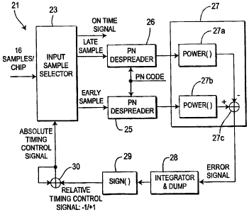
Referring to Figure 2, a block diagram of a CTL 21 in accordance with
the present invention is shown. The inputs are data samples with the
sampling rate of 16 times the chip rate. It should be noted that although
specific data rates are set forth herein, these data rates are provided by way
of
example only. For example, although data sample rates may vary, sampling
rates of 8 and 16 are typical sample rates. In another example using 16 times
the rate of sampling, for every 16 samples one of the samples will be an
"on-time" synchronized sample which will be used for despreading,
demodulation and rake combining. The CTL 21 will track this timing and
select the on-time sample. To achieve this goal, the CTL 21 will use early and
late samples.
CTL 21 includes an input sample selector 23, an early sample
pseudonoise (PN) despreader 25, a late sample PN despreader 26, an early-late
detector 27, an integration and dump circuit 28, a sign calculator 29 and a
summer 30. The input sample selector 23 provides early and late samples to
the PN despreaders 25, 26 which, in turn, provide signals to the early-late
detector 27. The early-late detector 27 includes a late power calculator 27a,
an
early power calculator 27b and a summer 27c. The output of the early-late
detector 27 is an error signal which is provided to the integrator and dump
circuit 28. The output of the integrator and dump circuit 28 is sent to the
sign
calculator 29. The sign calculator 29 outputs a 1 signal that is input to
the
-4-
CA 02653507 2009-02-09
=`...
summer 30. The summer 30 converts the relative timing control signal (i.e. -
141) to an absolute timing control signal taking into account previous
results.
The output of the summer 30 is sent to the input sample selector 23 to form
the loop.
The integration function that is performed by the integrator in the
integration and dump circuit 28 accumulates the signal power and to improve
the signal-to-noise ratio. After the signal is integrated for a defined or
predetermined period of time, the integration value is output. In order to
integrate the signal for the next time period, the signal in the integrator is
first cleared. Accordingly, the procedure in which the integrator integrates
signal discontinuously between different periods of time is called
"integration
and dump." The integration interval is selected to be a pilot symbol interval.
In a preferred embodiment, the pilot symbol interval is a predetermined
number of chips, which in the exemplary embodiment is 256 chips.
The CTL 21 operates by first despreading the early samples and the late
samples. The early and late samples are despread by a PN sequence that is
known to the receiver. The despread data is denoted as s, (k) and Sr (k) for
early and late samples respectively, where se (k) and Sr (k) are complex
numbers, and k represents kth data in the time domain. The early-late
detector 27 uses despread data, or data symbols, to generate an error signal,
which can be obtained noncoherently using Equation (1):
Er (k) = S, (k)l 2 - S, (k)12
Equation (1)
For each N error signals Er(k), where (N>1), a control signal Cowill be
generated according to the sign of the sum of these N error signals Er(k),
which
can be expressed as:
-5-
CA 02653507 2009-02-09
=`..
N
Co = sign Y EY (k)
k=1
Equation (2)
This control signal Co is used to adjust all on-time, early and late
samples either forward or backward by M samples. Typically M=1 or 2, or
MJ16 chip, which is typically 1/16 chip or 1/8 chip. The data rate of this
control
signal C. is therefore N times lower than the data rate of error signals
Er(k).
Still referring to Figure 2, in some instances the transmitted data can
be estimated. If this is the case (i.e., the transmitted data can be
estimated),
this is done by first removing the modulated data is from the despread early
signal and despread late signal. This results in:
Se(k) * a(k)* and
Equation (3)
Sj (k) * a(k)* , respectively,
Equation (4)
where a(k) is the transmitted symbol or an estimate of transmitted signal,
and ( )* represents the conjugate. Thereafter, N, despread early and late
signals with data removed are coherently summed to calculate the error signal
Er(k) that can be expressed by:
N 2 N 2
Er(k) = ISe(k)a(k)# - JS,(k)a(k)' Equation (5)
k=1 k=1
The despread data SQ(k) or S,(k) contains a demodulating symbol a(k)
that is {-1,+1} for BPSK modulation or 1-1,+1, j,+j} for QPSK modulation.
When the despread data SQ(k) or S,(k) is multiplied with the conjugate of a(k)
as in Equations (3) and (4), the a(k) component in the despread data Se(k) or
S,(k) will be "removed."
-6-
CA 02653507 2009-02-09
The data rate of the error signal Er(k) is Nl times lower than that of the
despread early or late signal since every N, despread early or late signal
generates one error signal. For every N error signals Er(k), where N>1, a
control signal Co is generated according to the sign of the sum of these N
error
signals, and the data rate of this control signal Co is Nl x N times lower
than
the data rate of error signals.
In either case, the error signal Er(k) is generated. Equation (1) uses one
despread data symbol to generate one error signal Er(k). Equation (5) uses N,
despread data symbols to generate one error signal Er(k). Therefore the data
rates of the error signals Er(k) are different by Nl times.
According to one embodiment of the present invention, both coherent
and non-coherent approaches are used. Coherent detection adds signals
coherently (i.e. sum the complex numbers directly) such as the sums in
Equation 5 (or as will be explained in detail hereafter, the inner sum in
Equation 7). Noncoherent detection adds signals noncoherently (i.e. sum the
power of complex numbers) such as the sum which will be explained with
reference to Equation 6. The difference between the two approaches is that
coherent detection has better performance than noncoherent detection.
However, in order to use coherent detection to obtain better performance, the
transmitted signal a(k) has to be known or estimated as performed in
Equation 5.
A second embodiment of a CTL 31 in accordance with the present
invention using low sampling rate input data is shown in Figure 3. This CTL
31 includes an interpolator 33, an early sample PN despreader 35, a late
sample PN despreader 36, an early-late detector 37, an integration and dump
circuit 38, a sign calculator 39 and a summer 40. The interpolator 33 provides
early and late samples to the PN despreaders 35, 36, which in turn provide
signals to the early-late detector 37. The early-late detector 37 includes a
late
-7-
CA 02653507 2009-02-09
signal power calculator 37a, an early signal power calculator 37b, and a
summer 37c. The output of the early-late detector 37 is an error signal Et(k)
which is provided to the integrator and dump circuit 38. The output of the
integrator and dump circuit 38 is sent to the sign calculator 39.
The sign calculator 39 outputs a 1 signal that is supplied to the
summer 40. The summer 40 converts the relative timing control signal (i.e. -
141) to an absolute timing control signal taking into account previous
results.
The output of the summer 40 is sent to the interpolator 33 to form the loop in
the same manner as depicted in Figure 2.
For low sampling rate input data, the sampling rate is typically two
samples per chip. In order to adjust the timing for on-time and early/late
samples forward or backward by a fraction of chip (for example 1/16 chip or
1/8
chip), the interpolator 33 is used to generate all on-time samples, and
early/late samples which are offset by such amount of time from the previous
samples.
As can be seen, the input data rates are different for the input sample
selector 23 shown in Figure 2 and the interpolator 33 shown in Figure 3. The
sample selector 23 selects which input samples to use according to the control
signal Co. Since the interpolator 33 has only two input samples per chip, it
has
to regenerate or interpolate the desired samples according to a control signal
input.
The CTL 21 of Figure 2 requires a high-speed analog-to-digital
converter (ADC). The CTL 31 of Figure 3 uses a low-speed ADC, which is
lower in cost, but CTL 31 also requires an extra interpolator to regenerate
the
desired samples. With CTL 21, a high data rate (i.e. 16 samples/chip) is used
and therefore a high speed ADC is required. With CTL 31, a low data rate (i.e.
2 samples/chip) is used and therefore a low speed ADC is required. The
different data rates are needed for different applications. For example, in
-8-
CA 02653507 2009-02-09
Figure 4, a low speed ADC is preferred because is uses 2 samples/chip and
interpolator 53.
In an exemplary embodiment corresponding to the UMTS FDD
standard, for uplink transmissions every slot of the dedicated physical
control
channel contains ten symbols (including pilot, transmit power control and
TFCI bits). Among these ten symbols, pilot symbols are known to the receiver,
but the power control and TFCI bits are unknown to the receiver. Suppose
that SEk,j and SLk,j denote the despread early and late signals for the jth
symbol in the kth slot. If the CTL 31 is updated every two frames (there are
15 slots per frame and 30 slots per two frames), then the control signal Co at
the output of the integration and dump circuit 38 using noncoherent
combining can be expressed as:
130 10
Ca = SIGN 1 1 JISEk,il' - I SLk,I z
k=1 j=1
Equation (6)
Alternatively CTL 31 coherently sums a number of early and late signals from
one slot, and then calculates the power and the error signal Er(k). Again if
the
CTL 31 is updated every two frames, then the control signal Co at the
integrator output can be expressed as:
30 Ni ~ N, ~
Co = SIGN SEk,j ak,j -~ SLk,j ak,j
k=1 j=1 j=1
Equation (7)
where ak j is the known pilot bit or the estimated power control/TFCI bit in
the jth symbol of the kth slot.
Some further alternatives are possible by implementing various
combinations of the following items: 1) using an input sample selector 23 (for
the high speed ADC as shown in Figure 2) or interpolator 33 (for the low speed
ADC as shown in Figure 3); 2) using a noncoherent error signal calculation as
-9-
CA 02653507 2009-02-09
in Equations 1 and 6 or using coherent error signal calculation as in
Equations
and 7; and 3) using error signal power as in Equations 1-5, 6 and 7 or using
error signal absolute value as in Equation 9. As explained above, Figure 2
uses an input sample selector, noncoherent error signal calculation, and error
5 signal power (Equation 1) and Figure 3 uses an interpolator, noncoherent
error
signal calculation and error signal power (Equation 1). Figure 4, explained
below, uses an interpolator, noncoherent error signal calculation and error
signal absolute value.
As explained above Equations (6) and (7) represent two different
methods to generate the error signal Er(k) as explained above. Equation (6)
uses noncoherent detection and uses the error signal generation in
Equation (1), and Equation (7) uses coherent detection and uses the error
signal generation in Equation (5). The "SIGN" is used to adjust the timing
forward or backward. When the sign of Equations (6) or (7) is positive, it
will
adjust the timing backward; whereas when the sign of Equations (6) or (7) is
negative, it will adjust the timing forward.
An embodiment of a CTL for UMTS FDD in accordance with the present
invention is shown in Figure 4. The CTL circuit 51 includes an interpolator
53, a delay circuit 54, early and late PN despreaders 55, 56, two magnitude
calculation circuits 57, 58 which calculate absolute values of the respective
signals, and a summer 59. Also included is an integrator and dump circuit 63,
a sign calculator 64 and a second summer 65. The interpolator 53 provides a
single early/late output to delay circuit 54, which provides an early signal
to
early PN despreader 55. The output of interpolator 53 is provided directly to
late PN despreader 56 and the outputs of the despreaders 55, 56 are provided
to respective magnitude calculation circuits 57, 58.
The circuit of Figure 4 uses the first error signal generation method-
described by Equations (1) and (6) because the early sample and late sample
are separated by exactly one chip interval, and the early sample can be
-10-
CA 02653507 2009-02-09
obtained from late sample by delaying one sample. Further, in Figure 4, the
square calculation performed by the early and late signal power calculators
37a, 37b is replaced with an absolute value calculation in order to simplify
the
hardware complexity.
If one compares Equation (9) with Equation (1), it will be noted that the
integrator and dump circuit 63 performs the summing as described in
Equation (6); and the sign calculator 64 resolves the sign (+ or -) as
described
in Equation (6). Since this sign generates a relative timing adjustment, a new
absolute timing signal is generated by summing the previous absolute timing
with the incoming relative adjustment. This is done in summer 65.
The absolute values (of the early and late despreaders 55, 56 calculated
in the magnitude calculation circuits 57, 58) are provided to the summer 59,
which provides an error signal Er(k) as its output to the integrator and dump
circuit 63 which and, in turn, outputs to the sign calculator 64. The output
from the sign calculator 64 hard limited to a 1 signal, which is supplied as
a
phase control signal to the interpolator 53, to form the loop.
The error signal AkJ is the difference of the absolute values of Ek,i and
LkJ, which can be expressed as:
A kj -JEk,i - JLk,.iI Equation (9)
The integrator and dump circuit 63 provides the magnitude of the error
signals and its output is hard-limited by the sign calculator 64 to either +1
or
-1 according to the sign of the summed error signals. This +1 or -1 is used to
adjust the timings of all punctual, early and late samples by 1/8 chip forward
or backward and is implemented by controlling the interpolator phase. This
interpolator phase is updated by subtracting the previous phase with the new
input data (+1 or -1).
The interpolator 53 uses four samples (with the sampling interval of a
half chip) to generate the punctual and late samples. The relationship
-11-
CA 02653507 2009-02-09
between the phase control signal (i.e. the interpolator output), the timing
offset and the interpolator coefficients is shown in Table 1. The early sample
is generated by delaying one sample of the previously generated late sample.
If the punctual sample is on phase "0," then the late sample will be on the
phase "2." If the punctual sample is on phase "x," then the late sample will
be
on phase "x+2."
Table 1. Interpolator Phase, Timing Offset and Coefficients.
Interpolato timing
Phase offset coefficient coefficient coefficient coefficient
(chips) 1 2 3 4
-6 -0.7500 0.0000 0.0000 0.0000 1.0000
-5 -0.6250 0.0547 -0.2578 0.6016 0.6016
-4 -0.5000 0.0625 -0.3125 0.9375 0.3125
-3 -0.3750 0.0391 -0.2109 1.0547 0.1172
-2 -0.2500 0.0000 0.0000 1.0000 0.0000
-1 -0.1250 -0.0391 0.2734 0.8203 -0.0547
0 0.0000 -0.0625 0.5625 0.5625 -0.0625
1 0.1250 -0.0547 0.8203 0.2734 -0.0391
2 0.2500 0.0000 1.0000 0.0000 0.0000
3 0.3750 0.1172 1.0547 -0.2109 0.0391
4 0.5000 0.3125 0.9375 -0.3125 0.0625
5 0.6250 0.6016 0.6016 -0.2578 0.0547
6 0.7500 1.0000 0.0000 0.0000 0.0000
The integrator and dump circuit 63 is reset every 30 slots during steady
tracking mode, and is reset every ten slots during the initial pull-in mode.
At
the beginning, the CTL 51 is in a "rough" timing position. It is desirable for
CTL 51 to react quickly to find the right timing position (initial pull-in
mode),
-12-
CA 02653507 2009-02-09
and then the CTL 51 will lock to this position and track any timing change
(tracking mode). During the first five frames after the finger is assigned to
the
CTL 51, the CTL 51 is assumed to be in the pull-in mode, and from the sixth
frame on, the CTL 51 is assumed to be in the tracking mode.
For the pull-in mode, the CTL 51 is updated every ten slots and all ten
pilot and data symbols are used per dedicated physical control channel
(DPCCH) slot. In this case the accumulator output Q can be expressed as:
10
Q=SIGN Y Y Akj
k=li=1 Equation (10)
For steady mode, the CTL 51 is updated every 30 slots (or two frames)
10 and all ten pilot and data symbols are used per DPCCH slot. The integrator
and dump circuit output 63 can be expressed as:
130 10
Q' = SIGN JY0k,j Equation (11)
k=1 j=1
Simulations of the results of CTL 51 tracking during a steady mode
were performed, The simulation parameters were as follows:
1) Both time and frequency drift is 0.613ppm;
2) The channel is AWGN channel;
3) Target SNR= -24 dB;
4) The CTL 51 is updated every two frames (30 slots);
5) For each CTL 51 updating, 1/8 chip forward or backward adjustment is
applied;
6) The maximum timing error is calculated;
7) The root-square of mean square timing error (RMSE) is calculated;
8) Both noncoherent and coherent combining are considered;
9) For noncoherent combining, ten symbols per slot are used, and the error
signal calculation is same as Equation (6);
10) For coherent combining, only three pilot symbols per slot are used, and
the error signal calculation is same as Equation (7) with N1=3;
-13-
CA 02653507 2009-02-09
11) A simplified scheme is simulated, which uses the absolute value instead
of power of early and late signals.
Figure 5 is a graph showing simulated timing tracking at SNR = -24dB
using coherent detection. By applying Equation (7), a noncoherent combining
of ten pilot symbols per slot is achieved. Figure 6 is a graph showing
simulated timing tracking at SNR = -24dB using non-coherent detection.
Figure 7 shows the results of a simplified error signal calculation in
accordance with the present invention using Equation (11). Since the error
signal calculation in both Equation (6) for noncoherent combining and
Equation (7) for coherent combining need to calculate the power of complex
numbers, this power calculation is very complicated in a hardware
implementation. In order to reduce the hardware complexity, the magnitude
calculation is used instead of the power calculation.
If all ten pilot and data symbols are used for noncoherent combining in
each slot and the CTL is updated every two frames (30 slots), then the
accumulator output can be expressed as:
Q"= SIGN jjjEk,j - Lk,j I Jk=1 j=1
Equation (12)
If only first three pilot symbols are used for coherent combining in each
slot and the CTL is updated every two frames (30 slots), then the accumulator
output can be expressed as:
130 3 3
Q=SIGN I I EkJ - I Lk,.i
k=1 1j=1 j=1
Equation (13)
Table 2 is a set of performance comparisons of the RMSE of difference
CTL schemes. In this table, three CTL schemes were compared. One is the
-14-
CA 02653507 2009-02-09
noncoherent combining using ten symbols per slot; the second is the coherent
combing using three pilot symbols per slot; and the third is the simplified
noncoherent combining using ten symbols per slot. For the target
SNR = 24dB, the three schemes perform closely. When the SNR is -34dB, the
coherent combining performs worst because fewer symbols are used. The
simplified scheme is worse than the non-simplified version.
Table 2. The RMSE of difference CTL schemes
Noncoherent Coherent Simplified
combining using combining using noncoherent
symbols per 3 symbols per slot combining using
slot 10 symbols per slot
SNR = - 1.63 1.51 1.52
24dB
SNR = - 2.18 2.27 2.17
30dB
SNR = - 3.07 5.15 4.03
34dB
10 Each CTL tracks one finger independently. When two multipaths (or
fingers) are within one and half chip, the two CTLs for the two fingers will
interfere with each other and therefore degrades the CTL tracking
performance. According to a particular aspect of the invention, a joint CTL
scheme is used to reduce the interference from each other. Without loss of
generality, it is possible to take an approach that there are two multipaths.
-15-
CA 02653507 2009-02-09
The received signal r(t) can be expressed as
r(t) = h, (t)s(t) + h2 (t)s(t - z) Equation (14)
where s(t) is the useful signal, s(t) akg(t - kT) , ak is the information
k=-w
symbol and g(t) is the signal waveform. h, (t) is the channel gain of the
first
path and h2 (t) is the channel gain of the second path. r is the relative
delay
between the two fingers. Note that the additive white Gaussian noise is not
considered in Equation (14).
When the relative delay between two adjacent fingers is less than
1.5 chip, the two independent CTLs will interfere with each other as shown in
Figure 8. It should be noted that triangle waveform is used for demonstration
only and is not necessarily used in practice. Due to the interference, the
performance of the two CTLs will degrade. The sample of the late signal of the
first finger will contain the interference hZ g(z - T/ 2) from the second
finger,
and the sample of the early signal of the second finger will contain the
interference h,g(z - T/ 2) from the first finger. The sample of the late
signal of
the first finger S,lst(k) is:
S; s` (k) = h, (k)g(T / 2) + h2 (k)g(z - T/ 2) Equation (15)
and the sample of the early signal of the second finger Se2nd(k) is:
Se "d (k) = h, (k)g(z - T / 2) + hz (k)g(T / 2) . Equation (16)
Figure 9 is a block diagram of joint CTL scheme 100. The components
are similar to Figure 4, but with a joint error signal calculator 102
operating
as part of two CTL circuits 103, 104.
CTL circuit 103 includes an interpolator 113, a delay circuit 114, early
and late PN despreaders 115, 116, two magnitude calculation circuits 117, 118
which calculate absolute values of the respective signals, and a summer 119.
Also included is an integrator and dump circuit 123, a sign calculator 124,
and
a second summer 125. The interpolator 113 provides a single early/late output
-16-
CA 02653507 2009-02-09
to delay circuit 114, which provides an early signal to early PN despreader
115. The output of interpolator 113 is provided directly to late PN despreader
116 and the outputs of the despreaders 115, 116 are provided to respective
magnitude calculation circuits 117, 118. CTL circuit 104 includes an
interpolator 133, a delay circuit 134, early and late PN despreaders 135, 136,
two magnitude calculation circuits 137, 138 which calculate absolute values of
the respective signals, and a summer 139. Also included is an integrator and
dump circuit 143, a sign calculator 144, and a second summer 145. The
interpolator 133 provides a single early/late output to delay circuit 134,
which
provides an early signal to early PN despreader 135. The output of
interpolator 133 is provided directly to late PN despreader 136 and the
outputs
of the despreaders 135, 136 are provided to respective magnitude calculation
circuits 137, 138.
As can be seen, the relative delay r between the two fingers can be
obtained from two CTLs. As is the case with the circuit of Figure 4, the
circuit
of Figure 9 uses the first error signal generation method-described by
Equations (1) and (6) because the early sample and late sample are separated
by exactly one chip interval and the early sample can be obtained from late
sample by delaying one sample. An absolute calculation is used in order to
simplify the hardware complexity.
According to particular aspects of the present invention, the following
two methods are effective to cancel interference:
Method 1: If the channel gains h, (t) and h2 (t), are known, the inference
is cancelled by subtracting the interference from useful signal. The error
signals are generated as
E,'.s` (k) = ISes` (k) 2 - IS, s` (k) - h2 (k)g(r - T / 2) 2 Equation (17)
Er n`' (k) = Se "`` (k) - h, (k)g(z - T / 2) 2 - S; ` d (k)12 Equation (18)
The control signal Co is calculated using Equation (2).
-17-
CA 02653507 2009-02-09
Method 2: If the channel gains h, and h2 are not known, but the power
of the two fingers is known, which are the means of the channel gains h, Z and
h2 2, El h, 12 and E hz 2. Since:
S;S`(k)z =EIh, 2 g2 (T/2)+Eh2 2 g2 (z-T12) Equation (19)
N k_l
Send (k) 2 =Elh, 2 g2(z-T/2)+Ejh2 12 g2 (T/2) Equation (20)
N k=,
The control signal Co is calculated as follows with the interference
removed.
Cos` = sign 1 ~ ~SQ's` (k) ~ - 1 11S~ s` (k) ~ - Ejh2 12 g2 (z - T / 2)
Equation (21)
N k_, N k_,
Co"d =sign 1 ~Send(k)2 ~ 5~11~r(k)2 -Eh, 2 g2(z-T/2)
N k=, N kL==,
Equation (22)
The present invention is useful in cellular mobile systems. In one
preferred embodiment, the invention is implemented in a base station
transmission as controlled by a radio network controller or a Node B transmit
controller. It is understood, however, that the invention can be used for a
wide
variety of spread spectrum communications transmissions.
-18-