Note: Descriptions are shown in the official language in which they were submitted.
CA 02653761 2013-08-07
TITLE: SYSTEMS AND METHODS FOR PERFORMING MEASUREMENTS OF ONE
OR MORE MATERIALS
BACKGROUND OF THE INVENTION
1. Field of the Invention
This invention generally relates to systems and methods for performing
measurements of
one or more materials. In particular, the invention relates to a system and
method configured to
transfer one or more materials to an imaging volume of a measurement device
from one or more
storage vessels, to image the one or more materials in the imaging volume, to
substantially
immobilize the one or more materials in the imaging volume, or some
combination thereof.
2. Description of the Related Art
The following descriptions and examples are not admitted to be prior art by
virtue of
their inclusion within this section.
Instrumentation typically employed in flow cytometry provide viable systems
for
measuring one or more characteristics of (or "interrogating") internally dyed
microspheres (or
other particles) to which are coupled fluorescent dyes, fluorophores, or
fluorescent tags. The
fluorescent dyes, fluorophores, or fluorescent tags coupled to the
microspheres may indicate
and/or be approximately proportional to a biological reaction that has taken
place at the surface
of the microspheres. Examples of such instrumentation are described in U.S.
Patent No.
5,981,180 to Chandler et al. The Luminex 100 line of instruments, which are
commercially
available from Luminex Corporation, Austin, Texas, essentially are flow
cytometers capable of
achieving substantially high sensitivity and specificity.
Flow cytometers typically include several relatively sophisticated and
expensive devices
such as semiconductor lasers, precision syringe pumps, photomultiplier tubes
(PMT), and
avalanche photo diodes. While performance of such systems is substantially
high, the cost of the
instruments can be prohibitive for some markets. Additionally, flow cytometers
are physically
large, heavy and relatively fragile, and typically a trained technician must
be on hand at the
installation site to perform alignment of the flow cytometers. Flow cytometers
also utilize
relatively large volumes of sheath fluid to hydrodynamically focus the
particle stream into a
relatively narrow core.
CA 02653761 2013-08-07
Imaging using detectors such as charged coupled device (CCD) detectors are
employed in several currently available instruments used in biotechnology
applications. Many
of the commercially available systems are configured to image target human (or
other animal)
cells. Such systems are not utilized to generate images using different
wavelengths of light for
determining the identity of the cells or subset to which the cells belong. For
multiplexed
applications in which CCD detectors are used to measure fluorescent emission
of cells, the
subset or class of cells or other particles is based on the absolute position
of the fluorescence
emission within the image rather than the characteristics of the fluorescence
emission such as
wavelength composition.
Accordingly, it would be desirable to develop systems and methods for
performing
measurements of one or more materials that are less expensive than currently
used systems, that
have less complex optical configurations that are more mechanically stable
than currently used
systems thereby making shipping and installation of the systems easier, that
are smaller than
currently used systems, that are more sensitive than currently used systems,
that have shorter
acquisition times and higher throughput than currently used systems, that
utilize fewer
consumables such as sheath fluid than currently used systems, that enable a
final wash of the one
or more materials for which the measurements are to be performed, or some
combination thereof.
SUMMARY OF THE INVENTION
The problems outlined above are largely addressed by the system and methods of
the
present invention. The system includes a fluid handling subsystem for loading
and removing
samples from the device and for cleaning the device or samples. An optics
subsystem includes
an illumination configuration, such as a plurality of LED's and a collection
configuration, such
as one or more imaging sensors. Finally, an immobilization subsystem is
employed to hold the
sample during the measurement interval. In a preferred form, the
immobilization subsystem
includes a magnet and the sample includes magnetic beads where the magnet can
be selectively
operated to immobilize the magnetic beads during imaging. In another form, the
position of the
collection configuration and the illumination configuration in relation to the
sample during
imaging is optimized.
The following description of various embodiments of systems and methods is not
to be
construed in any way as limiting the subject matter of the invention.
One embodiment relates to a system configured to transfer one or more
materials to an
imaging volume of a measurement device from one or more storage vessels. This
system may be
2
CA 02653761 2008-11-28
WO 2007/143615 PCT/US2007/070345
further configured as described herein. Another embodiment relates to a method
for transferring
one or more materials to an imaging volume of a measurement device from one or
more storage
vessels. In this method, transferring the one or more materials may be
performed as described
further herein. In addition, this method may include any other step(s)
described herein.
Furthermore, this method may be performed by any of the systems described
herein.
An additional embodiment relates to a system configured to image one or more
materials
in an imaging volume of a measurement device. This system may be further
configured as
described herein. A further embodiment relates to a method for imaging one or
more materials
in an imaging volume of a measurement device. Imaging the one or more
materials may be
performed as described further herein. In addition, this method may include
any other step(s)
described herein. Furthermore, this method may be performed by any of the
systems described
herein.
Yet another embodiment relates to a system configured to substantially
immobilize one or
more materials in an imaging volume of a measurement device. This system may
be further
configured as described herein. Still another embodiment relates to a method
for substantially
immobilizing one or more materials in an imaging volume of a measurement
device.
Substantially immobilizing the one or more materials may be performed as
described further
herein. In addition, this method may include any other step(s) described
herein. Furthermore,
this method may be performed by any of the systems described herein.
A further embodiment relates to a system configured to transfer one or more
materials to
an imaging volume of a measurement device from one or more storage vessels, to
image the one
or more materials in the imaging volume, to substantially immobilize the one
or more materials
in the imaging volume, or some combination thereof This system may be further
configured as
described herein. Another embodiment relates to a method for transferring one
or more
materials to an imaging volume of a measurement device from one or more
storage vessels,
imaging the one or more materials in the imaging volume, substantially
immobilizing the one or
more materials in the imaging volume, or some combination thereof
Transferring, imaging, and
substantially immobilizing the one or more materials may be performed as
described further
herein. In addition, this method may include any other step(s) described
herein. Furthermore,
this method may be performed by any of the systems described herein.
3
CA 02653761 2008-11-28
WO 2007/143615 PCT/US2007/070345
BRIEF DESCRIPTION OF THE DRAWINGS
Other objects and advantages of the invention will become apparent upon
reading the
following detailed description and upon reference to the accompanying drawings
in which:
Fig.1 is a block diagram of the fluid handling subsystem of the present
invention;
Fig. 2 is a block diagram depicting the optical configuration of a device of
the present
invention;
Fig. 3 is vertical cross section with parts broken away of a device of the
present invention
showing one version of the block diagram of Fig. 2;
Fig. 4 is a perspective view of the device of Fig. 3;
Figs. 5-7 are schematic diagrams illustrating block diagrams of various
embodiments of a
system configured to transfer one or more materials to an image volume of a
measurement
device from one or more storage vessels;
Fig. 8 is a schematic diagram illustrating an isometric side view of one
embodiment of a
system configured to image one or more materials in an imaging volume of a
measurement
device;
Figs. 9-15 are schematic diagrams illustrating a side view of various
embodiments of a
system configured to image one or more materials in an imaging volume of a
measurement
device;
Figs. 16-17 are schematic diagrams illustrating a side view of various
embodiments of an
illumination subsystem that may be included in embodiments of a system
configured to image
one or more materials in an imaging volume of a measurement device described
herein;
Figs. 18-20 are schematic diagrams illustrating a top view of various
embodiments of an
illumination subsystem that may be included in embodiments of a system
configured to image
one or more materials in an imaging volume of a measurement device described
herein;
Fig. 21 is a schematic diagram illustrating a side view of another embodiment
of a system
configured to image one or more materials in an imaging volume of a
measurement device and to
substantially immobilize the one or more materials in the imaging volume;
Figs. 22-23 are schematic diagrams illustrating a top view of various
embodiments of a
substrate on which one or more materials can be substantially immobilized in
an imaging volume
of a measurement device;
Figs. 24-25 are schematic diagrams illustrating a side view of various
embodiments of a
substrate on which one or more materials can be substantially immobilized in
an imaging volume
of a measurement device;
4
CA 02653761 2013-08-07
Fig. 26 is a schematic illustrating the collection and illumination angle
space; and
Fig. 27 is vertical profile view of an illumination module in accordance with
a preferred
embodiment of the device of the present invention.
While the invention is susceptible to various modifications and alternative
forms, specific
embodiments thereof are shown by way of example in the drawings and will
herein be described
in detail. It should be understood, however, that the drawings and detailed
description thereto
are not intended to limit the invention to the particular form disclosed.
DETAILED DESCRIPTION OF THE PREFERRED EMBODIMENTS
Although some embodiments are described herein with respect to particles,
beads, and
microspheres, it is to be understood that all of the systems and methods
described herein may be
used with particles, microspheres, polystyrene beads, microparticles, gold
nanoparticles,
quantum dots, nanodots, nanoparticles, nanoshells, beads, microbeads, latex
particles, latex
beads, fluorescent beads, fluorescent particles, colored particles, colored
beads, tissue, cells,
micro-organisms, organic matter, non-organic matter, or any other discrete
substances known in
the art. The particles may serve as vehicles for molecular reactions. Examples
of appropriate
particles are illustrated in U.S. Patent Nos. 5,736,330 to Fulton, 5,981,180
to Chandler et al.,
6,057,107 to Fulton, 6,268,222 to Chandler et al., 6,449,562 to Chandler et
al., 6,514,295 to
Chandler et al., 6,524,793 to Chandler et al., and 6,528,165 to Chandler. The
systems and
methods described herein may be used with any of the particles described in
these patents. In
addition, particles for use in method and system embodiments described herein
may be obtained
from manufacturers such as Luminex Corporation, Austin, Texas. The terms
"particles,"
"microspheres," and "beads" are used interchangeably herein.
In addition, the types of particles that are compatible with the systems and
methods
described herein include particles with fluorescent materials attached to, or
associated with, the
surface of the particles. These types of particles, in which fluorescent dyes
or fluorescent
particles are coupled directly to the surface of the particles in order to
provide the classification
fluorescence (i.e., fluorescence emission measured and used for determining an
identity of a
particle or the subset to which a particle belongs), are illustrated in U.S.
Patent Nos. 6,268,222 to
Chandler et al. and 6,649,414 to Chandler et al. The types of particles that
can be used in the
methods and systems described herein
5
CA 02653761 2013-08-07
also include particles having one or more fluorochromes or fluorescent dyes
incorporated into
the core of the particles. Particles that can be used in the methods and
systems described herein
further include particles that in of themselves will exhibit one or more
fluorescent signals upon
exposure to one or more appropriate light sources. Furthermore, particles may
be manufactured
such that upon excitation the particles exhibit multiple fluorescent signals,
each of which may be
used separately or in combination to determine an identity of the particles.
The embodiments described herein are capable of achieving substantially
equivalent or
better performance than that of a flow cytometer, while overcoming the issues
described in the
section above entitled "Description of the Related Art." The embodiments
described herein
include several configurations using two broad based imaging methods. For
fluorescence
detection or collection, a single sensor such as a photomultiplier tube (PMT)
or avalanche
photodiode (APD) per detected wavelength may be employed as commonly used in
flow
cytometers. However, the particularly preferred embodiments envision a one- or
two-
dimensional charge coupled device (CCD) or another suitable array detector for
fluorescence
5 detection. The excitation source may be configured to provide widespread
illumination (i.e.,
illumination provided over a relatively large area of the imaging volume of
the measurement
device (such as the entire imaging volume of the measurement device)
simultaneously) using
light emitted by light sources such as light emitting diodes (LEDs) and
delivered to one or more
materials in the imaging volume of the measurement device directly or via
fiber optics.
Alternatively, the excitation source may be configured to provide illumination
of a relatively
small spot in the imaging volume of the measurement device, and the system may
be configured
to scan the relatively small spot across the imaging volume. In this manner,
the illumination
may be configured as a relatively "tiny flying spot" of focused light
generated from one or more
LED's, one or more lasers, one or more other suitable light sources, or some
combination
thereof.
The embodiments described herein also provide a number of advantages over
other
systems and methods for performing measurements of one or more materials. For
example, the
embodiments described herein are advantageously less expensive than other
systems and
methods. In particular, in several configurations described herein, the
embodiments may include
a relatively inexpensive CCD as a photon detector rather than a PMT,
relatively simple LED's in
place of lasers, a relatively inexpensive pump in place of precision syringe
pump to move fluids,
or some combination thereof.
Thus, the aggregate cost of the embodiments described herein can
6
CA 02653761 2008-11-28
WO 2007/143615 PCT/US2007/070345
be reduced by approximately an order of magnitude. In addition, the
embodiments described
herein are advantageous due to a substantially simpler optical configuration
than that typically
used for flow cytometry thereby rendering the embodiments described herein
substantially
mechanically stable. Such mechanical stability enables shipping the system
embodiments
described herein via a standard shipping service (e.g., a UPS-type service).
Furthermore, such
mechanical stability allows the system embodiments described herein to be
installed by a user
who may or may not be a technically adept service person. Moreover, the
embodiments
described herein are advantageous since the system embodiments can be
substantially small
(e.g., conceivably the size of a pocket camera).
Another advantage of the embodiments described herein is that the embodiments
provide
the ability to integrate photons over a time period much longer than a few
microseconds as is
typical using a laser-based flow cytometer type system. Therefore, the
embodiments described
herein are capable of detecting particles with fewer molecules of fluorescence
on the surface or
otherwise coupled thereto than currently used systems and methods. As such,
the embodiments
described herein may advantageously have a higher sensitivity than other
currently used systems
and methods. In addition, the embodiments described herein may have
substantially shorter
measurement acquisition times and therefore higher throughput than currently
used systems. For
example, in embodiments configured to use a CCD/LED "flood-illumination"
configuration,
acquisition of sample measurements is faster since an entire sample or an
entire population of
particles can be measured in two or three images or "pictures," rather than
serially particle by
particle. In another example, for users that desire a relatively high
throughput solution, a
CCD/LED based system provides a comparatively inexpensive system, and in
several instances,
can be operated in parallel to quickly process a single microtiter plate or
other sample.
Yet another advantage of the embodiments described herein is that sheath fluid
is not
used to hydrodynamically focus the particles as in flow cytometry. Still
another advantage of the
embodiments described herein is that a final "wash" of the one or more
materials for which
measurements are to be performed is possible within the system to remove free
fluorochromes or
other materials that will interfere with the measurements from the liquid
surrounding the
particles thereby lowering the background light detected by the measurement
device (e.g., by the
imaging sensors of the measurement device).
The description of the embodiments provided further herein is generally
divided into
three subsections, in which different system embodiments are described. For
example, one
subsection relates to fluidic configurations that may be included in the
system embodiments
7
CA 02653761 2008-11-28
WO 2007/143615 PCT/US2007/070345
described herein. The fluid handling configurations can be used to introduce
or transfer the one
or more materials (e.g., beads and other reagents or beads after one or more
reactions have been
allowed to take place on the surface of the beads) to an imaging volume of the
measurement
device from one or more storage vessels. Another subsection relates to optical
configurations
that may be included in the system embodiments described herein. In general,
the different
optical configurations include different combinations of excitation sources
and photon detectors,
sometimes known herein as illumination modules and collection modules. An
additional
subsection relates to particle immobilization configurations and methods that
may be included
in, or used by, the system embodiments described herein. The systems described
herein may
lo include such particle immobilization configurations since in an imaging
system, the particles
preferably do not move substantially during the measurement interval. Note
that any
combination of the system configurations described in the three subsections
above may be
combined to produce a final imaging system embodiment.
Turning now to the drawings, it is noted that the figures are not drawn to
scale. In
particular, the scale of some of the elements of the figures is greatly
exaggerated to emphasize
characteristics of the elements. It is also noted that the figures are not
drawn to the same scale.
Elements shown in more than one figure that may be similarly configured have
been indicated
using the same reference numerals.
First Preferred Embodiment
Figs. 1-4 are illustrative of the first embodiment. This embodiment relates
generally to a
system configured to transfer one or more materials to an imaging volume of a
measurement
device from one or more storage vessels. As noted above, the system has three
major
components: fluid handling 6, optic configuration 8, and particle
immobilization subsystem (not
shown in Fig. 1). Fig. 1 shows the functional components of the fluid handling
subsystem while
Fig. 2 illustrates the functional components of the optics subsystem.
In the fluid handling subsystem of Fig. 1, samples are transferred into
imaging volume 10
of the measurement device from sample storage vessel 12. The imaging volume
may be
configured as an imaging chamber 10, which may have any suitable configuration
known in the
art. Storage vessel 12 may be configured as a micro titer plate or any other
suitable sample
container known in the art.
The system also includes a bi-directional pump 14 configured to draw fluid
into a storage
reservoir and to later expel fluid from the storage reservoir into the imaging
volume of chamber
8
CA 02653761 2008-11-28
WO 2007/143615 PCT/US2007/070345
10. Pump 14 may have any suitable configuration known in the art. Since the
particles are
substantially immobilized during the exposure time as described further
herein, pulse-free flow
such as that obtained from an expensive syringe pump is not required for the
system
embodiments described herein. A sufficient reservoir can be formed out of a
length of tubing 16
between pump 14 and sample valve 18. Such a reservoir is commonly called a
"sample loop."
The tubing may have any suitable configuration. The function of sample valve
18 is to connect a
sample probe 15 to the reservoir (sample loop 16) when aspirating from storage
vessel 12 (e.g.,
the micro titer plate) and to connect the reservoir to the imaging chamber 10
when dispensing.
Sample valve 18 may include any suitable valve known in the art.
Wash valve 20 is utilized at the pump end of the storage reservoir to allow
fresh water (or
other suitable reagent) from storage vessel 22 to flow to the imaging volume
of imaging chamber
10. Wash valve 20 may include any suitable valve known in the art. In
alternative
embodiments, the sample and wash valves could be combined into a single valve
(not shown).
Pump 14 may also be configured to transfer the one or more materials and any
other fluid in
imaging volume 10 to waste vessel 24. Waste vessel 24 may have any suitable
configuration
known in the art.
There are two primary modes of operating the fluid handling subsystem 6 to
load a
sample in the imaging chamber 10, namely a load procedure with sample wash and
a load
procedure without sample wash. Referring to Figs. 1 and 2, the load procedure
with NO sample
wash generally occurs as follows:
Clean System
1) Pump Valve 20 to position a.
2) Load Drive Solution.
3) Pump Valve 20 to position c.
4) Sample Valve 18, mover from position 1 to 3.
5) Move magnet 262 back (away from imaging chamber 10).
6) Push Drive Solution through chamber to clean chamber 10.
7) Sample Valve 18, position 1 to 2.
8) Push Drive solution through Probe 15to clean Probe.
9
CA 02653761 2008-11-28
WO 2007/143615 PCT/US2007/070345
Load Sample
1) Pump Valve 20 to position a.
2) Load Drive Solution.
3) Pump Valve 20 to position c.
4) Sample Valve 18, position 1 to 2.
5) Lower probe 15 into sample well 12.
6) Load a sample into sample loop 16.
7) Raise probe 15 and pull until air is at sample valve 18 and entire sample
is in sample loop
16.
8) Sample Valve 18, position 1 to 3.
9) Move magnet 262 forward (toward imaging chamber 10).
10) Push Sample from sample loop 16 into imaging chamber 10 capturing magnetic
beads.
11) Take Images with the sample immobilized.
Clean System
1) Pump Valve 20 to position a.
2) Load Drive Solution.
3) Pump Valve 20 to position c.
4) Sample Valve 18, position 1 to 3.
5) Move magnet 262 back (away from imaging chamber 10).
6) Push Drive Solution through chamber 10 to clean chamber.
7) Sample Valve 18, position 1 to 2.
8) Push Drive solution through Probe 15 to clean Probe.
The load procedure with sample wash generally occurs as follows:
Clean System
1) Pump Valve 20 to position a.
2) Load Drive Solution.
3) Pump Valve 20 to position c.
4) Sample Valve 1 to 3.
5) Move magnet 262 back (away from chamber 10).
6) Push Drive Solution through chamber 10 to clean chamber.
CA 02653761 2008-11-28
WO 2007/143615 PCT/US2007/070345
7) Sample Valve 18, position 1 to 2.
8) Push Drive solution through Probe 15 to clean Probe.
Preload Wash Solution
1) Pump Valve 20 to position b.
2) Load Wash Solution.
3) Pump Valve 20 to position c.
4) Sample Valve 1 to 3.
5) Push Wash Solution through chamber.
6) Sample Valve 18, position 1 to 2.
7) Push Wash solution through Probe 15(sample loop 16 and probe 15 preloaded
with Wash
Solution).
Load Sample
1) Pump Valve 20 to position a.
2) Load Drive Solution.
3) Pump Valve 20 to position c.
4) Sample Valve 18, position 1 to 2.
5) Lower probe 15 into well 12.
6) Load Sample into sample loop 16.
7) Raise probe 15 and pull until air is at sample valve and entire sample is
in sample loop
16.
8) Sample Valve 18, position 1 to 3.
9) Move magnet 262 forward (toward chamber 10).
10) Push Sample from sample loop 16 into chamber 10 capturing magnetic beads.
11) Push Wash Solution in sample loop 16 behind sample over captured magnetic
beads to
"Wash" beads.
12) Take Images with the sample immobilized.
Clean System
1) Pump Valve 20 to position a.
2) Load Drive Solution.
3) Pump Valve 20 to position c.
11
CA 02653761 2008-11-28
WO 2007/143615 PCT/US2007/070345
4) Sample Valve 18, position 1 to 3.
5) Move magnet 262 back (away from chamber 10).
6) Push Drive Solution through chamber 10 to clean chamber.
7) Sample Valve 18, position 1 to 2.
8) Push Drive solution through Probe 15 to clean Probe.
An advantage of using the second loading procedure where the sample is
"washed" is to
remove from the surrounding solution fluorochromes that are not bound to the
surface of a bead.
For the convenience of processing, some assays do not perform this final wash
step, resulting in
excitation of the extraneous fluorophores, which results in a "background"
signal when the assay
response from beads is measured. Thus, these no-wash assays have a poorer
limit of detection
than washed assays.
Unlike a flow cytometer, the system of the present invention inherently
provides the
ability to dispense with the fluid surrounding the beads, thereby washing away
the free
fluorochromes. This is possible because the beads are magnetically attached to
the substrate
(when the magnet is brought into contact with the back of the chamber), and
will not move if a
new "fresh" fluid is injected into the chamber, thereby displacing the
fluorochrome laden liquid.
Turning to Fig. 2, the optics subsystem 8 is broadly illustrated. This
subsystem 8
includes magnetic element 262 positioned on the side of imaging chamber 10
opposite the optics
of the system. Magnetic element 262 may include any suitable magnetic element
known in the
art such as a permanent magnet or an electromagnet that can be used to
generate a suitable
magnetic field. In this manner, dyed particles, e.g. beads, with embedded
magnetite may be used
such that the particles can be substantially immobilized in imaging chamber
10(e.g., at the
bottom of the chamber) using a magnetic field generated by magnetic element
262 at the side of
the chamber. Although magnetic element 262 is shown adjacent to imaging
chamber 10in Fig.
2, (see also Fig. 8 where magnetic element 264 is be in contact with (or
coupled to) imaging
chamber 1 Oon the side of the imaging chamber opposite the optical elements of
the system) the
magnetic element may be selectively spaced from the imaging chamber lOas shown
in Fig. 21.
Magnetic element 262 may be further configured as described above. In
addition, although Figs.
2, 8 and 21 show one magnetic element positioned proximate the imaging
chamber, it is to be
understood that the system may include more than one magnetic element, each of
which is
positioned proximate the side of the imaging chamber opposite the optics of
the system.
12
CA 02653761 2013-08-07
After signal acquisition by the measurement device, the magnetic field may be
removed
(e.g., by using a solenoid to move a permanent magnet or by turning an
electromagnet on and off
with a switch), and the particles may exit the imaging chamber 42, while new
particles from the
next sample are brought into the chamber 42. The particles in the imaging
chamber 10may be
removed and particles may be introduced to the imaging chamber using any of
the embodiments
described herein. The system shown in Fig. 2 may be further configured as
described herein.
The simplest imaging chamber 10 design is an imaging chamber that has a
relatively
smooth internal surface on the side of the imaging chamber proximate the
magnetic element such
that the beads are randomly distributed across this internal surface as the
magnet 262 pulls them
down. However, the imaging chamber lOcan also be designed to "hold" the beads
in particular
spots when the magnetic field is applied as described in more detail herein.
Figures 3 and 4 are depictions of what a measurement device in accordance with
the
present invention might look like incorporating the functional components
described in Figures 1
and 2.
Broadly speaking, the method of operating the measurement device of Figures 1
¨4
involves exposing the analytes of interest to a bead population to create a
sample, which is stored
in a sample vessel 12 as shown in Fig. 1. The sample is loaded into an imaging
chamber 10,
using, e.g. the sample handing steps described above. The sample is
immobilized in the imaging
chamber 10 by the selective operation of the magnet 262. Optionally, the
immobilized sample
can be washed to remove extraneous fluorospheres. With the sample immobilized
in the
chamber 10, the illumination module (LED's 44, 46) is operated to excite the
sample. The
imaging sensor 72 (CCD) captures the image and the image is processed (See,
e.g. U.S. Patent
Application Serial No. 60/719,010 entitled "Methods and Systems for Image Data
Processing"
filed September 21, 2005 by Roth). The magnet 262 releases the sample and the
device is
cleaned.
It is believed that the position of the imaging sensors 72 in relation to the
LED's 44, 46,
chamber 10 and magnet 262 can be optimized for imaging beads in accordance
with the present
invention. Beads have distinct characteristics, namely the dye within the
beads and reporter
molecules on the beads, both absorb and re-emit photons in no preferred
direction (uniformly
over all angles). The positions of the illumination by the LED's 44, 46 and
imaging sensors
(CCD 72) is chosen to optimize the "angle space" of any beads in the Field of
View (FOV) of
the imaging sensors (any beads that can be seen by the CCD 72). Since the
magnet 262 is on the
back of the chamber 10, the angle space available for the illumination and
imaging systems is a
13
CA 02653761 2008-11-28
WO 2007/143615 PCT/US2007/070345
hemisphere above the magnet. This is illustrated in Fig. 26 where "collection"
310 is the solid
angle collected by the imaging sensors 72 and "illumination angle space" 312
is the space that
the illumination modules can occupy. The more coverage over this illumination
angle space 312
by the illumination optics (LED's 44, 46 in Fig. 2), the more power imparted
on the beads during
imaging. Similarly, the higher the collection angle (Numerical Aperture) over
the illumination
angle space 312, the more flux the imaging lens 52 (Fig. 2) can collect and
deliver to the imaging
sensor 72 (CCD detector). A balance must be made between the angles allocated
for the imaging
sensors and the illumination system.
For low-cost manufacturability, the imaging lens 52 practical limit for
numerical aperture
is around 0.3 for a magnification of 4. For higher magnifications, the
numerical aperture of
imaging lens 52 could increase while maintaining the same cost guidelines.
Other factors that
effect the cost of the lens 52 are Field of View and broadness of waveband. A
numerical
aperture of 0.3 is roughly 35 degrees full angle.
For the positioning of the illumination module, e.g. the LED's 44, 46, the
limit may be
the LED's brightness as well as the cost of the excitation filters 47. The
etendue of the LED will
dictate what of the bead's angle space is needed to provide the maximum LED
flux over the field
of view (FOV). (Etendue is the Area of the source multiplied by the solid
angle of the source: it
defines the geometry characteristics of the emitted flux.) If the FOV is
relatively large, the angle
space required will be lower and therefore more LED's can be used. However,
more LED's will
add cost to the system. Again, a balance between costs vs. performance must be
determined.
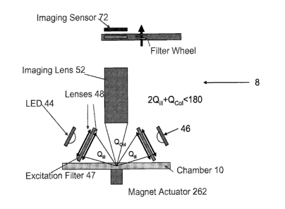
Comparing Figs. 2 and 27, the first embodiment includes an illumination module
consisting of lens, filters, and one or more LED's 44/46, as shown in Fig. 27.
As shown in Fig.
27, associated with each LED 44 is a lens system comprising two normal
refractive lenses 314.
The lenses 314 are used to collect as much light from the LED 44 as possible
and pseudo-
collimate it through the filter 316. Though one normal refractive lens 314 can
be used, the
collected angle is much less, thus leading to an inefficient illumination
system and a preference
for two or more lenses 314.
Normal refractive lens 314 are used prior to the filter 316 because there is
inherently
scatter at the edges of the fresnel lens grooves. Scattered light can pass
through the filter 316 at
non-optimal angles and increase the out-of-band background at the image. This
would lead to
increased background noise. The fresnel lens 318 is used after the filter 316
to re-focus the light
onto the chamber 10. Some blurring may be necessary to ensure uniformity at
the image plane.
The fresnel lens 318 is used because of cost as well as physical extent. The
fresnel lens 318 is
14
CA 02653761 2008-11-28
WO 2007/143615 PCT/US2007/070345
relatively thin. The primary cost component in the illumination module of Fig.
27 is the
excitation filter 316. The molded plastic refractive lenses 314 as well as the
fresnel lens 318 are
low cost. The LED 44 is also inexpensive.
Conservation of brightness dictates that the etendue must be preserved in an
optical
system to maximize efficiency. The etendue (in air) = Aco, where A is the area
and co is the
solid angle. The ramification is that the image size along with the imaging
optics magnification
dictates the field of view of the illumination module of Fig. 27. Using the
brightness equation,
the angle space needed for the illumination module can be calculated from the
FOV of the optics.
This angle space allows for the determination of the minimum number of LED's
necessary to
provide the maximum flux (power) to the FOV. More LED's will not increase the
power to the
FOV. Optimizing the angle space utilized by the illumination and imaging
systems can be
accomplished by applying the brightness equation. However, in the system of
Figs. 2-4, other
tradeoffs must also be made such as cost and performance.
The first embodiment depicted in Figs. 2-4 is configured to substantially
immobilize the
beads in an imaging volume of chamber 10 is shown in Fig. 2. Magnetic element
262 is
positioned on the side of imaging chamber 10 opposite the optics of the system
(illumination and
collection modules). Magnetic element 262 may include any suitable magnetic
element known
in the art such as a permanent magnet or an electromagnet that can be used to
generate a suitable
magnetic field. In this manner, dyed beads with embedded magnetite may be used
such that the
beads can be substantially immobilized in imaging chamber 10 (e.g., at the
bottom of the
chamber) using a magnetic field generated by magnetic element 262 at the back
side of the
chamber. Although magnetic element 262 is shown adjacent the imaging chamber
10 in Fig. 2,
magnetic element 262 may be in contact with (or coupled to) or spaced from
imaging chamber
10 on the side of the imaging chamber opposite the optical elements of the
system.
After signal acquisition by the measurement device, the magnetic field may be
removed
(e.g., by using a solenoid to move a permanent magnet or by turning an
electromagnet on and off
with a switch), and the beads may exit the imaging chamber 10, while new beads
from the next
sample are brought into the chamber 10. The beads in the imaging chamber 10
may be removed
and beads may be introduced to the imaging chamber 10 using any of the
embodiments
described herein.
The design of the imaging chamber 10 in Fig. 2 is a relatively smooth internal
surface on
the side of the imaging chamber 10 proximate the magnetic element 262 such
that the beads are
randomly distributed across this internal surface as the magnet pulls them
down. However, the
CA 02653761 2008-11-28
WO 2007/143615 PCT/US2007/070345
imaging chamber 10 can also be designed to "hold" the beads in particular
spots when the
magnetic field is applied as described in additional embodiments herein.
Additional Embodiments
Another embodiment of such a system in accordance with the present invention
is shown
in Fig. 5. In this embodiment, samples are transferred into imaging volume 10
of the
measurement device (not shown in Fig. 5) from storage vessel 12. The imaging
volume may be
configured as an imaging chamber, which may have any suitable configuration
known in the art.
Storage vessel 12 may be configured as a microtiter plate or any other
suitable sample container
lo known in the art.
The system also includes single bi-directional pump 14 configured to draw
fluid into a
storage reservoir and to later expel fluid from the storage reservoir into the
imaging volume.
Pump 14 may have any suitable configuration known in the art. Since the
particles are
substantially immobilized during the exposure time as described further
herein, pulse-free flow
such as that obtained from an expensive syringe pump is not required for the
system
embodiments described herein. A sufficient reservoir can be formed out of a
length of tubing 16
between pump 14 and sample valve 18. Such a reservoir is commonly called a
"sample loop."
The tubing may have any suitable configuration. The function of sample valve
18 is to connect a
sample probe (not shown) to the reservoir when aspirating from storage vessel
12 (e.g., the
microtiter plate) and to connect the reservoir to the imaging chamber when
dispensing. Sample
valve 18 may include any suitable valve known in the art.
Wash valve 20 is utilized at the pump end of the storage reservoir to allow
fresh water (or
other suitable reagent) from storage vessel 22 to flow to the imaging volume.
Wash valve 20
may include any suitable valve known in the art. Note that the sample and wash
valves could be
combined into a single valve (not shown). Pump 14 may also be configured to
transfer the one
or more materials and any other fluid in imaging volume 10 to waste vessel 24.
Waste vessel 24
may have any suitable configuration known in the art. The embodiment shown in
Fig. 5 may be
further configured as described herein.
Another embodiment of a system configured to transfer one or more materials to
an
imaging volume of a measurement device from one or more storage vessels is
shown in Fig. 6.
In this configuration, the system includes pump 26 configured to draw liquid
directly into
imaging volume 10 from storage vessel 12 (e.g., the sample probe) and then out
to waste vessel
24. Pump 26 may include any suitable pump known in the art such as a
peristaltic pump.
16
CA 02653761 2008-11-28
WO 2007/143615 PCT/US2007/070345
Imaging volume 10, storage vessel 12, and waste vessel 24 may be configured as
described
above. Optional valve 28 between storage vessels 12 and 22 (e.g., a microtiter
plate or another
suitable sample container) and imaging volume 10 may be configured to change
positions
depending on whether sample is to be transferred to the imaging volume or if
wash fluid is to be
transferred to the imaging volume (e.g., if the wash function is to be
performed). Valve 28 may
include any suitable valve known in the art. In addition, storage vessel 22
may be configured as
described above.
The embodiment shown in Fig. 6 is advantageous over the embodiment shown in
Fig. 5
since this embodiment saves the cost of a temporary reservoir, includes one
less valve, and
lo utilizes a pump configured to move fluids in only one direction. A
disadvantage of the
embodiment shown in Fig. 6 over the embodiment shown in Fig. 5 is the
inability of the
embodiment shown in Fig. 6 to cleanse the sample probe with wash fluid,
without which may
lead to increased "carry over" from sample to sample. The embodiment shown in
Fig. 6 may be
further configured as described herein.
An additional embodiment of a system configured to transfer one or more
materials to an
imaging volume of a measurement device from one or more storage vessels is
shown in Fig. 7.
This embodiment has a configuration that is similar to the configuration of
the embodiment
shown in Fig. 6, with the exception that sample/wash valve 28 of the
embodiment shown in Fig.
6 is replaced by two valves 30 and 32. Valves 30 and 32 may include any
suitable valves known
in the art. For example, valves 30 and 32 may include open/closed type valves
configured to
separately and simultaneously allow fluid from storage vessels 12 and 22,
respectively, to be
transferred into imaging volume 10. Storage vessels 12 and 22 and imaging
volume 10 may be
configured as described herein.
Providing separate wash and sample paths (i.e., one path from storage vessel
12 to
imaging volume 10 and another separate path from storage vessel 22 to imaging
volume 10) in
this manner makes it possible to achieve all of the aspects of the embodiment
shown in Fig. 6
and adds the ability to mix wash fluid and/or one or more reagents to the one
or more materials
to be measured (i.e., the sample solution) as the sample is transferred into
imaging volume 10.
Mixing wash fluid and/or one or more reagents to the one or more materials
(e.g., the sample) as
the one or more materials are transferred to the imaging volume may be
performed to dilute the
sample such that the particles are distributed farther apart within the
imaging volume (e.g.,
farther apart on the floor of the imaging chamber) thereby enabling better
statistical separation of
17
CA 02653761 2008-11-28
WO 2007/143615 PCT/US2007/070345
the particles, which will result in more accurate measurement of each
particle. The embodiment
shown in Fig. 7 may be further configured as described herein.
Another embodiment relates to a method for transferring one or more materials
to an
imaging volume of a measurement device from one or more storage vessels.
Transferring the
one or more materials may be performed as described further herein. In
addition, this method
may include any other step(s) described herein. For example, the method may
include mixing
wash fluid and/or one or more reagents to the one or more materials as the one
or more materials
are transferred to the imaging volume. Furthermore, this method may be
performed by any of
the systems described herein (e.g., by the embodiments shown in Figs. 5-7).
Figs. 8-9 illustrate one embodiment of a system configured to image one or
more
materials in an imaging volume of a measurement device. This system embodiment
includes
detectors 34, 36, and 38. Detectors 34, 36, and 38 may be CCD cameras or any
other suitable
imaging devices known in the art. Each of the detectors may have the same
configuration or
different configurations. Each of the detectors may be configured to detect
light (e.g., light
fluoresced from particles 40 in imaging volume defined by imaging chamber 42)
at a different
wavelength or wavelength band. In addition, each of the detectors may be
configured to
generate images or "capture fluorescent pictures" of particles 40 in imaging
chamber 10(e.g.,
particles resting on the bottom of imaging chamber 42). Imaging chamber 10may
have any
suitable configuration known in the art.
The system also includes light sources 44 and 46 configured to emit light
having different
wavelengths or different wavelength bands (e.g., one of the light sources may
be configured to
emit red light and the other light source may be configured to emit green
light). The light
emitted by light sources 44 and 46 may include, for example, light in any part
of the visible
wavelength spectrum. Light sources 44 and 46 may include LEDs or any other
suitable light
sources known in the art. Light sources 44 and 46 are arranged above the
periphery of imaging
chamber 42. In addition, the light sources are arranged above the imaging
chamber such that
each light source directs light to particles 40 in imaging chamber lOat
different directions.
The system also includes filters 48 and 50 coupled to light sources 44 and 46,
respectfully. Filters 48 and 50 may be bandpass filters or any other suitable
spectral filters
known in the art. In this manner, the system may use light sources 44 and 46
and filters 48 and
50 to sequentially illuminate the particles with different wavelengths or
different wavelength
bands of light. For example, red light may be used to excite classification
dyes (not shown) that
may be internal to the particles, and green light may be used to excite
reporter molecules (not
18
CA 02653761 2008-11-28
WO 2007/143615 PCT/US2007/070345
shown) coupled to the surface of the particles. Since the classification
illumination is dark
during reporter measurements (i.e., in the above example, red light is not
directed to the particles
while green light is directed to the particles), the analyte measurement
sensitivity of the system
will not be reduced due to crosstalk from out of band light.
The system may also include single lens 52 positioned at the center (or
approximately the
center) of the illumination "ring." Lens 52 may include any suitable
refractive optical element
known in the art. Lens 52 is configured to image light scattered and/or
fluoresced from the
particles onto one or more monochrome CCD detector(s) (e.g., detectors 34, 36,
and 38) via one
or more optical elements, which may include one or more dichroic and one or
more optical
bandpass filters. For example, light exiting lens 52 is directed to dichroic
filter 54, which may
include any suitable dichroic optical element known in the art. Dichroic
filter 54 is configured to
reflect light of one wavelength or wavelength band and to transmit light of
other wavelengths or
wavelength bands. Light reflected by dichroic filter 54 is directed to filter
56, which may be a
bandpass filter or other suitable spectral filter. Light exiting filter 56 is
directed to detector 34.
Light transmitted by dichroic filter 54 is directed to dichroic filter 58,
which may include
any suitable dichroic optical element known in the art. Dichroic filter 58 may
be configured to
reflect light of one wavelength or wavelength band and to transmit light of
other wavelengths or
wavelength bands. Light transmitted by dichroic filter 58 is directed to
filter 60, which may be a
bandpass filter or other suitable spectral filter. Light exiting filter 60 is
directed to detector 36.
Light reflected by dichroic filter 58 is directed to filter 62, which may be a
bandpass filter or
other suitable spectral filter. Light exiting filter 62 is directed to
detector 38.
Furthermore, although the system shown in Fig. 9 includes two light sources,
it is to be
understood that the system may include any suitable number of light sources.
For example, as
shown in Fig. 8, the system may include four light sources (e.g., light
sources 44, 45, 46, and 47)
arranged around the periphery of lens 52. Light sources 44, 45, 46, and 47 may
include any of
the light sources described herein. In this manner, light sources 44, 45, 46,
and 47 may be
configured to provide an illumination "ring" surrounding lens 52.
Although the system shown in Figs. 8-9 includes three detectors configured to
image
light scattered and/or fluoresced from the particles at different wavelengths
or wavelength bands,
it is to be understood that the system may include two or more detectors. For
example, the
system may include two or more CCD detectors (and optionally fixed filters)
that can be used to
simultaneously measure the classification channel(s) and reporter channel(s)
thereby providing
higher throughput for the measurements along with additional hardware cost.
19
CA 02653761 2013-08-07
The system shown in Figs. 8-9 is, therefore, configured to generate a
plurality or series of
images representing the fluorescent emission of particles 40 at several
wavelengths of interest.
In addition, the system may be configured to supply a plurality or series of
digital images
representing the fluorescence emission of the particles to a processor (i.e.,
a processing engine).
The system may or may not include the processor (not shown). The processor may
be
configured to acquire (e.g., receive) image data from detectors 34, 36, and
38. For example, the
processor may be coupled to detectors 34, 36, and 38 in any suitable manner
known in the art
(e.g., via transmission media (not shown), each coupling one of the detectors
to the processor,
via one or more electronic components (not shown) such as analog-to-digital
converters, each
coupled between one of the detectors and the processor, etc.).
Preferably, the processor is configured to process and analyze these images to
determine
one or more characteristics of particles 40 such as a classification of the
particles and
information about a reaction taken place on the surface of the particles. The
one or more
characteristics may be output by the processor in any suitable format such as
a data array with an
entry for fluorescent magnitude for each particle for each wavelength.
Specifically, the
processor may be configured to perform one or more steps of a method for
processing and
analyzing the images. Examples of methods for processing and analyzing images
generated by a
system such as that shown in Figs. 8-9 are illustrated in U.S. Patent
Application Serial No.
60/719,010 entitled "Methods and Systems for Image Data Processing" filed
September 21, 2005
by Roth. The systems described herein may be further configured as described
in this patent
application. In addition, the methods described herein may include any step(s)
of any of the
method(s) described in this patent application.
The processor may be a processor such as those commonly included in a typical
personal
computer, mainframe computer system, workstation, etc. In general, the term
"computer
system"
may be broadly defined to encompass any device having one or more processors,
which executes
instructions from a memory medium. The processor may be implemented using any
other
appropriate functional hardware. For example, the processor may include a
digital signal
processor (DSP) with a fixed program in firmware, a field programmable gate
array (FPGA), or
other programmable logic device (PLD) employing sequential logic "written" in
a high level
programming language such as very high speed integrated circuits (VHSIC)
hardware
description language (VHDL). In another example, program instructions (not
shown) executable
on the processor to perform one or more steps of the computer-implemented
methods described
CA 02653761 2008-11-28
WO 2007/143615 PCT/US2007/070345
in the above-referenced patent application may be coded in a high level
language such as C#,
with sections in C++ as appropriate, ActiveX controls, JavaBeans, Microsoft
Foundation Classes
("MFC"), or other technologies or methodologies, as desired. The program
instructions may be
implemented in any of various ways, including procedure-based techniques,
component-based
techniques, and/or object-oriented techniques, among others.
Program instructions implementing methods such as those described in the above-
referenced patent application may be transmitted over or stored on a carrier
medium (not shown).
The carrier medium may be a transmission medium such as a wire, cable, or
wireless
transmission link. The carrier medium may also be a storage medium such as a
read-only
memory, a random access memory, a magnetic or optical disk, or a magnetic
tape.
Another embodiment relates to a method for imaging one or more materials in an
imaging
volume of a measurement device. Imaging the one or more materials may be
performed as
described further herein. In addition, this method may include any other
step(s) described
herein. Furthermore, this method may be performed by any of the systems
described herein.
Another embodiment of a system configured to image one or more materials in an
imaging volume of a measurement device is shown in Fig. 10. This system
embodiment
includes imaging chamber 42, light sources 44 and 46, filters 48 and 50, and
lens 52, which may
be configured as described above with respect to Figs. 8-9. In this
embodiment, however, the
system includes substrate 64 that includes filters 66, 68, and 70. Filters 66,
68, and 70 may
include bandpass filters or any other suitable spectral filters known in the
art. Substrate 64 may
include any appropriate substrate known in the art. Substrate 64 may be
coupled to one or more
devices that are configured to alter a position of the substrate and therefore
the filters in the
optical path of the light exiting lens 52. For example, the one or more
devices may be
configured to alter the position of the substrate by rotating the substrate.
As such, the substrate
and the filters therein may be configured as a circular, rotating filter
"wheel." However, the one
or more devices may be configured to alter the position of the substrate in
any other manner
known in the art.
Each of filters 66, 68, and 70 may be configured to transmit light of a
different
wavelength or a different wavelength band. As such, the wavelength or
wavelength band at
which an image of particles 40 is formed by detector 72 may vary depending on
the position of
the substrate and therefore the position of the filters in the optical path of
light exiting lens 52.
In this manner, a plurality of images of the particles may be formed
sequentially by imaging the
particles, altering the position of the substrate and therefore the filters,
and repeating the imaging
21
CA 02653761 2008-11-28
WO 2007/143615 PCT/US2007/070345
and altering steps until images at each wavelength or waveband of interest
have been acquired
by detector 72. In addition, although three filters are shown in substrate 64
in Fig. 10, it is to be
understood that the substrate may include any suitable number of filters. In
addition, the system
may include two or more such filters arranged in any other suitable
configuration such that the
system can alter the filter that is in the optical path of light exiting lens
52 in any other manner
known in the art. Detector 72 may include any of the detectors described
herein such as a CCD
array.
The system embodiment shown in Fig. 10 is, therefore, advantageous since the
system is
configured to use a single detector (e.g., a single CCD detector) with optical
filters unique to the
wavelengths or wavelength bands of interest (e.g., classification channel 1
(c11), classification
channel 2 (c12), reporter channel 1 (rp1), etc.) arranged on a circular
"filter wheel," which
provides a cost effective solution. However, this system is slower (i.e., has
a lower throughput)
than the system shown in Figs. 8-9 due to non-simultaneous, sequential
exposures used to form
the plurality of images. The system shown in Fig. 10 may be further configured
as described
herein.
An additional embodiment of a system configured to image one or more materials
in an
imaging volume of a measurement device is shown in Fig. 11. In this
embodiment, the system is
configured to have approximately double the imaging area of the systems shown
in Figs. 8-10
and to use a single detector and multiple filters that can be moved into and
out of the optical path
as described further above. In particular, the system shown in Fig. 11
includes a first set of light
sources 74 and 76, which may include any of the light sources described
herein. Light sources
74 and 76 are configured such that both light sources direct light to
approximately the same area
of imaging chamber 42, which may be configured as described herein. The system
also includes
a second set of light sources 78 and 80, which may include any of the light
sources described
herein. Light sources 78 and 80 are configured such that both light sources
direct light to
approximately the same area of imaging chamber 42, which is spaced from the
area of the
imaging chamber to which light sources 74 and 76 direct light.
The system shown in Fig. 11 also includes lens 82. Lens 82 is configured to
collect light
from the area of the imaging chamber to which light sources 74 and 76 direct
light. The light
collected by lens 82 may include fluorescent light and/or scattered light
emanating from the
particles or material(s) coupled thereto. Lens 82 may be further configured as
described herein.
The system also includes lens 84 that is configured to collect light from the
area of the imaging
chamber to which light sources 78 and 80 direct light. The light collected by
lens 84 may
22
CA 02653761 2008-11-28
WO 2007/143615 PCT/US2007/070345
include fluorescent light and/or scattered light emanating from the particles
or material(s)
coupled thereto. Lens 84 may be further configured as described herein. Lenses
82 and 84 may
be configured similarly or differently.
Light collected by lens 82 is directed to reflective optical element 86, which
may be any
suitable reflective optical element known in the art such as a mirror. The
position of reflective
optical element 86 may be relatively fixed. Light collected by lens 84 is
directed to reflective
optical element 88, which may be any suitable reflective optical element known
in the art such as
a mirror. The position of reflective optical element 88 may be relatively
fixed. Reflective
optical elements 86 and 88 may both be configured to direct light to
reflective optical element
90, which may include any suitable reflective optical element known in the art
such as a mirror.
Reflective optical element 90 may be coupled to one or more devices (not
shown) that are
configured to alter a position of the reflective optical element as shown by
arrow 92. The one or
more devices may include any suitable device(s) known in the art. In this
manner, reflective
optical element 90 may be configured as a "flip mirror," and the position of
the mirror may be
altered depending on which area of the imaging chamber is being imaged.
In particular, depending on the position of reflective optical element 90,
light from
reflective optical element 86 or reflective optical element 88 will be
directed to substrate 94.
Substrate 94 may be configured as described above with respect to substrate
64. In particular,
substrate 94 may include two or more filters (not shown in Fig. 11), and the
position of the
substrate and therefore the two or more filters with respect to reflective
optical element 90 may
be altered depending on the wavelength or wavelength band at which an image is
being formed.
Light transmitted by the two or more filters is directed to detector 96, which
may include a CCD
detector or any other detector described herein.
The system shown in Fig. 11 is, therefore, advantageous since this
configuration doubles
the imaging area and uses a single detector (e.g., a single CCD) and multiple
bandpass filters on
a rotating wheel. As described above, reflective optical element 90 (e.g., a
mirror) flips between
positions to direct the fluorescent light from lenses 82 and 84 to detector 96
in successive
exposures. As such, another advantage of the optical system shown in Fig. 11
is that double the
particles can be brought into the imaging chamber at once compared to the
number of particles
that can be brought into the imaging chambers of the systems shown in Figs. 4-
6 thereby saving
the time necessary to flip valves, etc. The system shown in Fig. 11 may be
further configured as
described herein.
23
CA 02653761 2008-11-28
WO 2007/143615 PCT/US2007/070345
A further embodiment of a system configured to image one or more materials in
an
imaging volume of a measurement device is shown in Fig. 12. This embodiment of
the system is
similar to that shown in Fig. 11 except that this embodiment is configured to
image particles that
are separated into two separate imaging chambers. In particular, light sources
74 and 76 are
configured to direct light to particles 98 in imaging chamber 100, and lens 82
is configured to
collect light from particles 98 in imaging chamber 100. Light sources 78 and
80 are configured
to direct light to particles 102 in imaging chamber 104, and lens 84 is
configured to collect light
from particles 102 in imaging chamber 104. Imaging chambers 100 and 104 may be
configured
as described herein. In addition, imaging chambers 100 and 104 may be
configured similarly or
differently. The system may also be advantageously configured such that while
particles are
being loaded into one of the imaging chambers, the system can be imaging light
scattered and/or
fluoresced from particles in the other imaging chamber thereby saving
acquisition time. The
system embodiment shown in Fig. 12 may be further configured as described
herein.
Another embodiment of a system configured to image one or more materials in an
imaging volume of a measurement device is shown in Fig. 13. This system
includes light
sources 106 and 108, which may include any of the light sources described
herein. Light sources
106 and 108 are configured to direct light to refractive optical element 110,
which may include
any suitable refractive optical element known in the art. Light exiting
refractive optical element
110 is directed to dichroic optical element 112, which is configured to
reflect light from
refractive optical element 110 to refractive optical element 114. Dichroic
optical element 112
may include any suitable dichroic optical element known in the art such as a
dichromatic mirror.
Refractive optical element 114 may include any suitable refractive optical
element known in the
art such as a lens. Refractive optical element 114 is configured to direct
light from dichroic
optical element 112 to particles 40 located in imaging chamber 42, which may
be configured as
described herein.
Fluorescent and/or scattered light emanating from particles 40 is collected by
refractive
optical element 114, which directs the fluorescent and/or scattered light to
dichroic optical
element 112. Dichroic optical element 112 is configured to transmit the
fluorescent and/or
scattered light. Therefore, the system shown in Fig. 13 is configured to
illuminate the particles
through refractive optical element 114 (e.g., an imaging objective lens) via
dichroic optical
element 112 (e.g., a dichromatic mirror) that is configured to separate the
excitation and the
emission light based upon wavelength. Such a configuration of the system is
advantageous since
it provides more uniform illumination across the field of view of the system.
24
CA 02653761 2008-11-28
WO 2007/143615 PCT/US2007/070345
The light transmitted by dichroic optical element 112 is directed to substrate
116, which
may include a plurality of filters (not shown in Fig. 13). Substrate 116 and
the plurality of filters
may be configured as described herein. Light exiting substrate 116 may be
directed to optional
refractive optical element 118, which may include any suitable refractive
optical element known
in the art such as a lens. Light exiting optional refractive optical element
118, or substrate 116 if
refractive optical element 118 is not included in the system, is directed to
detector 120, which
may include any of the detectors described herein. The system shown in Fig. 13
may be further
configured as described herein.
An additional embodiment (not shown) of a system configured to image one or
more
materials in an imaging volume of a measurement device includes a light source
configured to
emit light that the system is configured to scan across the imaging volume.
For example, the
system may include an optical element that is configured to alter the
direction of the light from
the light source such that the light scans over the imaging chamber. In such a
system, the light
source and/or the imaging chamber may or may not be substantially stationary.
Alternatively,
the system may be configured to alter a position of the light source (and
optical element(s)
associated with the light source) while the imaging chamber is substantially
stationary such that
the light scans over the imaging chamber. In another alternative, the system
may be configured
to alter a position of the imaging chamber while the light source (and optical
element(s)
associated with the light source) is substantially stationary such that the
light scans over the
imaging chamber. In a further alternative, the system may be configured to
alter a position of the
light source (and optical element(s) associated with the light source) and the
imaging chamber
such that the light scans over the imaging chamber. The system may be
configured to alter a
position of the light source (and optical element(s) associated with the light
source) and/or a
position of the imaging chamber in any manner known in the art.
In some such embodiments, the light source may include a laser, which may
include any
suitable laser known in the art. In addition, the system may include a single
detector and optical
filters, and the system may be configured to position one of the optical
filters in front of the
detector depending on the wavelength or wavelength band at which an image is
being formed.
In this manner, different images of light scattered and/or fluoresced from the
particles may be
formed at different wavelengths or wavelength bands while different optical
filters are positioned
in front of the detector. The detector may include any of the detectors
described herein. In
addition, the optical filters may include any of the optical filters described
herein. Furthermore,
the system may be configured to position one of the optical filters in front
of the detector as
CA 02653761 2008-11-28
WO 2007/143615 PCT/US2007/070345
described herein. Therefore, this configuration may use a scanning laser(s)
and a single detector
with optical filters unique to the wavelengths or wavelength bands of interest
(ell, c12,
classification channel 3 (c13), rpl, etc.).
Instead of illuminating the entire field of beads simultaneously, therefore,
the system may
be configured such that the laser(s) scan a spot smaller in diameter than the
beads across the
image plane thereby illuminating each particle separately. An advantage of
this embodiment
over configurations that include a two-dimensional CCD array is that the light
measured at any
time is guaranteed as being sourced from a single bead (assuming the beads are
far enough
apart). In contrast, in the flooded field (i.e., flood illumination) systems
shown in Figs. 4-6, light
detected by each pixel element of the detector (e.g., a CCD) may include some
contribution from
beads outside the area intended to be imaged by each pixel element. This
embodiment of the
system may be further configured as described herein.
A further embodiment (not shown) of a system configured to image one or more
materials in an imaging volume of a measurement device includes a light source
configured to
emit light that the system is configured to scan across the imaging volume.
The system may be
configured to scan the light across the imaging volume as described herein.
Like the system
embodiment described above, this configuration may use a scanning laser(s).
Therefore, instead
of illuminating the entire field of beads simultaneously, the laser(s) scan a
spot across the image
plane illuminating each particle separately. However, unlike the system
embodiment described
above, the system may include one or more PMT detector(s) and optical filters
unique to the
wavelength bands of interest (ell, c12, c13, rpl, etc.). The optical filters
may be positioned in
front of the one or more PMT detector(s) as described above. If the number of
PMTs included in
the system is less than the number of wavelengths or wavelength bands at which
an image is to
be acquired, the filters for one or more of the PMTs may be arranged as
described herein (e.g.,
on a circular filter wheel), and the desired filter can be rotated into view
before the scan
commences. This embodiment of the system may be further configured as
described herein.
An additional embodiment of a system configured to image one or more materials
in an
imaging volume of a measurement device is shown in Fig. 14. The system shown
in Fig. 14 may
be configured as described above with respect to Fig. 3 except that Fig. 14
includes a refractive
optical element that is different than refractive optical element 1 14 of the
system of Fig. 13 and a
different imaging chamber than the system of Fig. 13. In particular, the
system shown in Fig. 14
includes refractive optical element 122, which is coupled to imaging chamber
124. For instance,
refractive optical element 122 may be positioned in an opening formed in
imaging chamber 124
26
CA 02653761 2008-11-28
WO 2007/143615 PCT/US2007/070345
such that the surfaces of refractive optical element 122 and imaging chamber
124 proximate to
particles 40 are located in substantially the same plane. In addition, the
surfaces of refractive
optical element 122 and imaging chamber 124 that are in contact with each
other may be joined
in some manner. Refractive optical element 122 and imaging chamber 124 may be
further
configured as described herein.
The embodiment of the system shown in Fig. 14 is advantageous since this
configuration
employs a lens that is embedded in the imaging chamber to allow for maximum
numerical
aperture and thus maximum light collection from the sample. As described
further above, the
particles are illuminated through refractive optical element 122 (e.g., an
imaging objective lens)
via dichroic optical element 112 (e.g., a dichromatic mirror) that separates
the excitation and the
emission wavelengths. The embodiment of the system shown in Fig. 14 may be
further
configured as described herein.
An additional embodiment of a system configured to image one or more materials
in an
imaging volume of a measurement device is shown in Fig. 15. In this system,
imaging chamber
126 is configured as a waveguide imaging chamber. The waveguide imaging
chamber may be
configured as described herein. As shown in Fig. 15, the system includes light
sources 128 and
130. Light sources 128 and 130 may include any of the light sources described
herein. Light
sources 128 and 130 are configured to direct light to sides of imaging chamber
126 as opposed to
a top surface of imaging chamber 126 as in the above-described embodiment
configurations. In
some embodiments, the system includes filters 132 and 134 positioned between
light sources 128
and 130, respectively, and the imaging chamber. Filters 132 and 134 may
include bandpass
filters or any other suitable filters known in the art.
The system may also include lens 52, substrate 64 that includes filters 66,
68, and 70, and
detector 72, each of which may be configured as described above with respect
to Fig. 10.
However, unlike the system shown in Fig. 10, the system shown in Fig. 15
employs a waveguide
imaging chamber design to illuminate particles 40. This illumination
configuration allows lens
52 in the system of Fig. 15 to have a relatively short working distance with a
larger numerical
aperture than lens 52 in the system of Fig. 10. Such a lens will collect more
light from the beads
thereby decreasing exposure time. This illumination configuration may also
limit the amount of
incident light from the light sources collected by the lens. The embodiment of
the system shown
in Fig. 15 may be further configured as described herein.
Figs. 16-17 illustrate various embodiments of an illumination subsystem that
may be
included in embodiments of a system configured to image one or more materials
in an imaging
27
CA 02653761 2008-11-28
WO 2007/143615 PCT/US2007/070345
volume of a measurement device described herein. In particular, the
illumination subsystems
shown in Figs. 16-17 include light sources (e.g., LEDs) coupled to a waveguide
imaging
chamber in several possible manners. For example, illumination subsystem 136
includes light
source 138 that may include a Lambertian LED. The illumination subsystem also
includes
reflective optical element 140 and refractive optical element 142, which are
configured to focus
light from light source 138 to waveguide imaging chamber 144. Reflective
optical element 140
may include any suitable reflective optical element known in the art.
Refractive optical element
142 may include any suitable refractive optical element known in the art such
as a focusing lens.
The illumination subsystem may also include filter 146, which may be used as
an excitation
filter and may include any suitable filter described herein or known in the
art. In this manner,
illumination subsystem 136 may use a reflective optical element and/or a
refractive optical
element (e.g., a lens) to capture light (e.g., Lambertian LED light) and focus
the light onto the
excitation filter or side of the waveguide imaging chamber. This illumination
subsystem
embodiment may be further configured as described herein.
Illumination subsystem 148 shown in Fig. 12 includes light source 150 that may
include a
Lambertian LED. In this illumination subsystem, light source 150 is coupled
(e.g., butt coupled)
to waveguide imaging chamber 152 such that a surface of the light source is in
contact with
waveguide imaging chamber 152 or filter 154 if this filter is included in the
illumination
subsystem. Filter 154 may be used as an excitation filter and may include any
suitable filter
described herein or known in the art. In some embodiments, index matching
fluid and/or epoxy
156 is used to couple light source 150 to waveguide imaging chamber 152 or
filter 154. Index
matching fluid and/or epoxy 156 may include any suitable fluid and/or epoxy
known in the art.
The index matching fluid and/or epoxy may be used to improve the light
coupling from the light
source into the waveguide. This illumination subsystem embodiment may be
further configured
as described herein.
Illumination subsystem 158 shown in Fig. 17 includes light source 160 that may
be a side
emitting LED. Illumination subsystem 158 also includes reflective optical
element 162 and
refractive optical element 164, which are configured to focus light from light
source 160 to
waveguide imaging chamber 166. Reflective optical element 162 may include any
suitable
reflective optical element known in the art. Refractive optical element 164
may include any
suitable refractive optical element known in the art such as a focusing lens.
The illumination
subsystem may also include filter 168, which may be used as an excitation
filter and may include
any suitable filter described herein or known in the art. In this manner,
illumination subsystem
28
CA 02653761 2008-11-28
WO 2007/143615 PCT/US2007/070345
158 may use a reflective optical element and/or a refractive optical element
(e.g., a lens) to
capture light (e.g., edge emitting LED light) and focus the light onto the
excitation filter or side
of the waveguide imaging chamber. This illumination subsystem embodiment may
be further
configured as described herein.
Illumination subsystem 170 shown in Fig. 17 includes light source 172 that may
be a side
emitting LED. Light source 172 is disposed in through hole 174 formed in
waveguide imaging
chamber 176. Therefore, this illumination subsystem may couple a light source
(e.g., an edge
emitting LED) to a waveguide imaging chamber using a through hole in the
waveguide imaging
chamber. The illumination subsystem may also include filters 178 and 180,
which may be used
lo as excitation filters and may include any suitable filters described
herein or known in the art.
This illumination subsystem embodiment may be further configured as described
herein.
Figs. 18-19 illustrate various embodiments of an illumination subsystem that
may be
included in embodiments of a system configured to image one or more materials
in an imaging
volume of a measurement device described herein. In these illumination
subsystems, the
waveguide imaging chamber is coupled to multiple light sources (e.g., LEDs).
Fig. 18-19 show
a top down view of some of these designs using the waveguide coupling
described in Figs. 16-
17. For example, illumination subsystem 182 shown in Fig. 18 includes light
sources 184, which
may be Lambertian LEDs or edge emitting LEDs. Filters 186 may be disposed
between each
light source and waveguide imaging chamber 188. Filters 186 may include any of
the filters
described herein or known in the art. Since illumination subsystem 182 is
shown to include six
light sources arranged around a hexagonal shaped waveguide imaging chamber,
illumination
subsystem 182 is configured to have a hexagonal design with the edge coupling
described above.
However, the shape of the waveguide imaging chamber can be varied from a
simple rectangle,
to more complicated triangles, pentagons, hexagons, etc. to incorporate more
light sources. This
illumination subsystem is advantageous because three light sources configured
to emit light of
one color and three light sources configured to emit light of another color
(i.e., each wavelength
or wavelength band) can be coupled to the waveguide imaging chamber. Such an
illumination
subsystem configuration increases the intensity of the light directed to the
sample and provides
substantially uniform illumination. Illumination subsystem 182 may be further
configured as
described herein.
Illumination subsystem 190 shown in Fig. 18 includes light sources 192, which
may be
Lambertian LEDs or edge emitting LEDs. Filters 194 may be disposed between
each light
source and waveguide imaging chamber 196. Filters 194 may include any of the
filters
29
CA 02653761 2008-11-28
WO 2007/143615 PCT/US2007/070345
described herein or known in the art. The illumination subsystem may also
include reflective
optical elements and/or refractive optical elements 198, which may be
configured to focus light
from light sources 192 to filters 194 or the surface of waveguide imaging
chamber 196 if the
filters are not included in the illumination subsystem. The reflective optical
elements and/or
refractive optical elements may include any such suitable optical element(s)
known in the art.
Bead chamber 200 is disposed within waveguide imaging chamber 196. Bead
chamber 200 may
have any suitable configuration.
Since illumination subsystem 190 is shown to include six light sources
arranged around a
hexagonal shaped waveguide imaging chamber, illumination subsystem 190 is
configured to
have a hexagonal design with the edge coupling described above. In addition,
illumination
subsystem 190 is configured to direct the light from the light sources to bead
chamber 200 across
three intersecting rectangles 202 within the hexagonal shaped waveguide
imaging chamber to
better confine the light (e.g., the LED light) to the bead chamber. However,
the shape of the
waveguide imaging chamber can be varied from a simple rectangle, to more
complicated
triangles, pentagons, hexagons, etc. to incorporate more light sources. This
illumination
subsystem is also advantageous because three light sources configured to emit
light of one color
and three light sources configured to emit light of another color (i.e., each
wavelength or
wavelength band) can be coupled to the waveguide imaging chamber. Such an
illumination
subsystem configuration increases the intensity of the light directed to the
sample and provides
substantially uniform illumination. Illumination subsystem 190 may be further
configured as
described herein.
Illumination subsystem 204 shown in Fig. 19 includes light sources 206, which
may be
edge emitting LEDs. Light sources 206 are disposed in through holes 208 formed
in waveguide
imaging chamber 210. Filters 212 may be disposed between each light source and
waveguide
imaging chamber 210. Filters 212 may include any of the filters described
herein or known in
the art. Since illumination subsystem 204 is shown to include six light
sources arranged around
a hexagonal shaped waveguide imaging chamber, illumination subsystem 204 is
configured to
have a hexagonal design with through hole coupling of light sources such as
edge emitting LEDs
described above. However, the shape of the waveguide imaging chamber can be
varied from a
simple rectangle, to more complicated triangles, pentagons, hexagons, etc. to
incorporate more
light sources. This illumination subsystem is advantageous because three light
sources
configured to emit light of one color and three light sources configured to
emit light of another
color (i.e., each wavelength or wavelength band) can be coupled to the
waveguide imaging
CA 02653761 2008-11-28
WO 2007/143615 PCT/US2007/070345
chamber. Such an illumination subsystem configuration increases the intensity
of the light
directed to the sample and provides substantially uniform illumination.
Illumination subsystem
204 may be further configured as described herein.
Illumination subsystem 214 shown in Fig. 19 includes light sources 216, which
may be
edge emitting LEDs. Light sources 216 are disposed in through holes 218 formed
in waveguide
imaging chamber 220. Filters 222 may be disposed between each light source and
waveguide
imaging chamber 220. Filters 222 may include any of the filters described
herein or known in
the art. Bead chamber 224 is disposed within waveguide imaging chamber 220.
Bead chamber
224 may have any suitable configuration. Since illumination subsystem 214 is
shown to include
six light sources arranged around a hexagonal shaped waveguide imaging
chamber, illumination
subsystem 214 is configured to have a hexagonal design with the edge coupling
described above.
In addition, illumination subsystem 214 is configured to direct the light from
the light sources to
bead chamber 224 across three intersecting rectangles 226 within the hexagonal
shaped
waveguide imaging chamber to better confine the light (e.g., LED light) to the
bead chamber.
However, the shape of the waveguide imaging chamber can be varied from a
simple rectangle, to
more complicated triangles, pentagons, hexagons, etc. to incorporate more
light sources. This
illumination subsystem is also advantageous because three light sources
configured to emit light
of one color and three light sources configured to emit light of another color
(i.e., each
wavelength or wavelength band) can be coupled to the waveguide imaging
chamber. Such an
illumination subsystem configuration increases the intensity of the light
directed to the sample
and provides substantially uniform illumination. Illumination subsystem 214
may be further
configured as described herein.
Fig. 20 illustrates various embodiments of an illumination subsystem that may
be
included in embodiments of a system configured to image one or more materials
in an imaging
volume of a measurement device described herein. In the embodiments shown in
Fig. 20, the
waveguide imaging chamber is configured to allow each photon to make more then
one pass by
the bead chamber. For example, illumination subsystem 228 includes light
source 230, which
may include any of the light sources described herein. Light source 230 is
coupled to ring
waveguide imaging chamber 232 such that light emitted by light source 230
enters waveguide
imaging chamber 232. By using a ring waveguide imaging chamber design, the
photons that are
not absorbed by the beads on the first pass will travel around the ring and
come back to the
sample again. Such a waveguide imaging chamber configuration can greatly
increase the
intensity of the light on the beads. In addition, such a waveguide imaging
chamber configuration
31
CA 02653761 2008-11-28
WO 2007/143615 PCT/US2007/070345
will allow for shorter exposure times and the use of fewer light sources.
Illumination subsystem
228 may be further configured as described herein.
The basic ring waveguide imaging chamber included in illumination subsystem
228 can
be expanded to an oval approach to allow for the insertion of one or more bead
chamber regions.
For example, as shown in Fig. 20, illumination subsystem 234 includes light
source 236 that
may include any of the light sources described herein. Light source 236 is
coupled to oval
waveguide imaging chamber 238 such that light emitted by light source 236
enters waveguide
imaging chamber 238. Illumination subsystem 228 may be further configured as
described
herein.
Multiple light sources may also be coupled to an oval waveguide imaging
chamber to
allow light from two or more excitation sources to be coupled into the
waveguide imaging
chamber. For example, as shown in Fig. 20, illumination subsystem 240 includes
light sources
242 and 244, which may include any of the light sources described herein.
Light sources 242
and 244 are coupled to oval waveguide 246 at different positions within the
waveguide imaging
chamber such that the light emitted by light sources 242 and 244 enters
waveguide imaging
chamber 246 at different positions. As further shown in Fig. 20, waveguide
imaging chamber
246 includes bead chamber 248 in which beads may be disposed during the
measurements such
that the beads are illuminated by light from light sources 242 and 244 coupled
into the
waveguide imaging chamber. Illumination subsystem 240 may be further
configured as
described herein.
The oval waveguide imaging chamber can also be expanded to other shapes, like
a
triangle, a square, a pentagon, a hexagon, etc. For example, as shown in Fig.
20, illumination
subsystem 250 includes light sources 252, 254, 256, and 258, which may include
any of the light
sources described herein. Light sources 252, 254, 256, and 258 are coupled to
square waveguide
imaging chamber 260 at different positions within the waveguide imaging
chamber such that the
light emitted by light sources 252, 254, 256, and 258 enters waveguide imaging
chamber 260 at
different positions. Illumination subsystem 250 may be further configured as
described herein.
One embodiment of a system configured to substantially immobilize one or more
materials in an imaging volume of a measurement device is shown in Fig. 21.
This embodiment
of the system includes the system configured to image one or more materials in
an imaging
volume of a measurement device shown in Fig. 10. In addition, this system
includes magnetic
element 262 positioned on the side of imaging chamber lOopposite the optics of
the system.
Magnetic element 262 may include any suitable magnetic element known in the
art such as a
32
CA 02653761 2008-11-28
WO 2007/143615 PCT/US2007/070345
permanent magnet or an electromagnet that can be used to generate a suitable
magnetic field. In
this manner, dyed particles with embedded magnetite may be used in the
embodiments described
herein such that the particles can be substantially immobilized in imaging
chamber 10(e.g., at the
bottom of the chamber) using a magnetic field generated by magnetic element
262 at the back
side of the chamber. Although magnetic element 262 is shown spaced from
imaging chamber
10in Fig. 21, as shown in Fig. 8, magnetic element 264 may be in contact with
(or coupled to)
imaging chamber lOon the side of the imaging chamber opposite the optical
elements of the
system. Magnetic element 264 may be further configured as described above. In
addition,
although Figs. 8 and 21 show one magnetic element positioned proximate the
imaging chamber,
it is to be understood that the system may include more than one magnetic
element, each of
which is positioned proximate the side of the imaging chamber opposite the
optics of the system.
After signal acquisition by the measurement device, the magnetic field may be
removed
(e.g., by using a solenoid to move a permanent magnet or by turning an
electromagnet on and off
with a switch), and the particles may exit the imaging chamber, while new
particles from the
next sample are brought into the chamber. The particles in the imaging chamber
may be
removed and particles may be introduced to the imaging chamber using any of
the embodiments
described herein. The system shown in Fig. 21 may be further configured as
described herein.
The simplest imaging chamber design is an imaging chamber that has a
relatively smooth
internal surface on the side of the imaging chamber proximate the magnetic
element such that the
beads are randomly distributed across this internal surface as the magnet
pulls them down.
However, the imaging chamber can also be designed to "hold" the beads in
particular spots when
the magnetic field is applied. For example, internal surface 266 of an imaging
chamber shown in
Fig. 22 has a square pattern of etched recesses 268 formed therein such that
bead 270 is disposed
in one of the etched recesses upon application of a magnetic field as
described above. Therefore,
etched recesses 268 assist in separating the beads as the magnetic field is
applied. In addition,
the "etched" recesses may be formed by an etching process or any other
suitable process known
in the art. Furthermore, the configuration and arrangement of the etched
recesses may vary
depending on, for example, the size of the beads and the selected spacing
between the beads.
In another example, internal surface 272 of an imaging chamber shown in Fig.
23 has a
triangle pattern of etched recesses 274 such that bead 276 is disposed in one
of the etched
recesses upon application of a magnetic field as described above. Therefore,
etched recesses 274
assist in separating the beads as the magnetic field is applied. In addition,
the "etched" recesses
may be formed by an etching process or any other suitable process known in the
art.
33
CA 02653761 2013-08-07
Furthermore, the configuration and arrangement of the etched recesses may vary
depending on,
for example, the size of the beads and the selected spacing between the beads.
Although etched
recesses 268 and 274 shown in Figs. 22 and 23, respectively, are two-
dimensional in the sense
that the beads are confined by the recesses in two dimensions, these recesses
can be replaced by
trenches or any other suitable recesses that are configured to confine the
beads in only one
direction.
As shown in Fig. 24, bottom 276 of recessed regions 278 can be closed in the
sense that
there is no opening between bottom 276 of recessed regions 278 and substrate
280 that forms
one outer wall of the imaging chamber. Recessed regions 278 may include any of
the recessed
regions described above. As further shown in Fig. 20, bead 282 becomes
confined in recessed
region 278 when a magnetic field is applied to side 284 of the imaging
chamber. Although the
closed recessed regions shown in Fig. 24 are a simpler design, as shown in
Fig. 25, recessed
regions 286 can be formed with openings 288 between the bottom of structures
290 that form the
recessed regions and substrate 292 that forms the outer wall of the imaging
chamber. Openings
288 may be configured to allow for flow of wash fluid from behind the beads
(e.g., bead 294)
such that the wash fluid cannot force the beads out of the recessed regions.
Still another embodiment relates to a method for substantially immobilizing
one or more
materials in an imaging volume of a measurement device. Substantially
immobilizing the one or
more materials may be performed as described further herein. For example,
substantially
immobilizing the one or more materials in an imaging volume of a measurement
device may
include applying a magnetic field to one side of an imaging chamber that
defines the imaging
volume of the measurement device. In addition, this method may include any
other step(s)
described herein. Furthermore, this method may be performed by any of the
systems described
herein.
The system embodiments described herein configured to transfer one or more
materials
and/or to image one or more materials may or may not be configured to
substantially immobilize
the one or more materials according to embodiments described herein. For
example,
immobilization of the particles in the imaging volume may also be performed
using magnetic
attraction as described above, a vacuum filter substrate, or any other
appropriate method known
in the art. Examples of methods and systems for positioning microspheres for
imaging are
illustrated in U.S. Patent Application Serial No. 11/270,786 to Pempsell filed
November 9, 2005.
Regardless of the particle immobilization method, the particles are preferably
substantially
34
CA 02653761 2013-08-07
immobilized such that the particles do not move perceptibly during the
detector integration
period, which may be multiple seconds long.
Two or more of the system embodiments described herein can be combined into a
single
embodiment such that the single embodiment provides all of the advantages of
the two or more
system embodiments. For example, a further embodiment relates to a system
configured to
transfer one or more materials to an imaging volume of a measurement device
from one or more
storage vessels, to image the one or more materials in the imaging volume, to
substantially
immobilize the one or more materials in the imaging volume, or some
combination thereof. The
system may be configured to transfer the one or more materials as described
herein, to image the
one or more materials as described herein, to substantially immobilize the one
or more materials
as described herein, or some combination thereof. This system may be further
configured as
described herein.
Accordingly, another embodiment relates to a method for transferring one or
more
materials to an imaging volume of a measurement device from one or more
storage vessels,
imaging the one or more materials in the imaging volume, substantially
immobilizing the one or
more materials in the imaging volume, or some combination thereof
Transferring, imaging, and
substantially immobilizing the one or more materials may be performed as
described further
herein. In addition, this method may include any other step(s) described
herein. Furthermore,
this method may be performed by any of the systems described herein.
The measurements described herein generally include image processing for
analyzing one
or more images of particles to determine one or more characteristics of the
particles such as
numerical values representing the magnitude of fluorescence emission of the
particles at multiple
detection wavelengths. Subsequent processing of the one or more
characteristics of the particles
such as using one or more of the numerical values to determine a token ID
representing the
multiplex subset to which the particles belong and/or a reporter value
representing a presence
and/or a quantity of analyte bound to the surface of the particles can be
performed according to
the methods described in U.S. Patent Nos. 5,736,330 to Fulton, 5,981,180 to
Chandler et al.,
6,449,562 to Chandler et al., 6,524,793 to Chandler et al., 6,592,822 to
Chandler, and 6,939,720
to Chandler et al. In one example, techniques described in U.S. Patent No.
5,981,180 to
Chandler et al. may be used with the fluorescent measurements described herein
in a
multiplexing scheme in which the particles are classified into subsets for
analysis of multiple
analytes in a single sample.
CA 02653761 2013-08-07
It will be appreciated to those skilled in the art having the benefit of this
disclosure that
this invention is believed to provide systems and methods for performing
measurements of one
or more materials. Further modifications and alternative embodiments of
various aspects of the
invention will be apparent to those skilled in the art in view of this
description. Accordingly,
this description is to be construed as illustrative only and is for the
purpose of teaching those
skilled in the art the general manner of carrying out the invention. It is to
be understood that the
forms of the invention shown and described herein are to be taken as the
presently preferred
embodiments. Elements and materials may be substituted for those illustrated
and described
herein, parts and processes may be reversed, and certain features of the
invention may be utilized
independently, all as would be apparent to one skilled in the art after having
the benefit of this
description of the invention.
36