Note: Descriptions are shown in the official language in which they were submitted.
CA 02654185 2008-12-03
WO 2007/145720 PCT/US2007/010499
METHOD AND APPARATUS FOR LOW RANGE BIT DEPTH ENHANCEMENT
FOR MEMS DISPLAY ARCHITECTURES
BACKGROUND OF THE INVENTION
Field of the Invention
[0001] The field of the invention relates to microelectromechanical systems
(MEMS).
Description of the Related Art
[0002] Microelectromechanical systems (MEMS) incl'ude micro mechanical
elements, actuators, and electronics. Micromechanical elements may be created
using
deposition, etching, and/or other micromachining processes that etch away
parts of
substrates and/or deposited material layers or that add layers to form
electrical and
electromechanical devices. One type of MEMS device is called an
interferometric
modulator. As used herein, the term interferometric modulator or
interferometric light
modulator refers to a device that selectively absorbs and/or reflects light
using the
principles of optical interference. In certain embodiments, an interferometric
modulator
may comprise a pair of conductive plates, one or both of which may be
transparent and/or
reflective in whole or part and capable of relative motion upon application of
an
appropriate electrical signal. = In a particular embodiment, one plate may
comprise a
stationary layer deposited on a substrate and the other plate may comprise a
metallic
membrane separated from the stationary layer by an air gap. As described
herein in more
detail, the position of one plate in relation to another can change the
optical interference
of light incident on the interferometric modulator. Such devices have a wide
range of
applications, and it would be beneficial in the art to utilize and/or modify
the
characteristics of these types of devices so that their features can be
exploited in
improving existing products and creating new products that have not yet been
developed.
SUMMARY OF THE INVENTION
[0003] The system, method, and devices of the invention each have several
aspects, no single one of which is solely responsible for its desirable
attributes. Without
limiting the scope.of this invention, its more prominent features will now be
discussed
briefly. After considering this discussion, and particularly after reading the
section
entitled "Detailed Description of Certain Embodiments" one will understand how
the
features of this invention provide advantages over other display devices.
CA 02654185 2008-12-03
WO 2007/145720 PCT/US2007/010499
[0004] In certain embodiments, a light modulator device comprises a first
electrical conduit, a second electrical conduit electrically isolated from the
first conduit, a
first display element configured to communicate with the first conduit and the
second
conduit, and a second display element configured to communicate with the first
conduit
and the second conduit. The first display element is in an actuated state when
a voltage
difference between the first conduit and the second conduit has a magnitude
greater than a
first actuation voltage. The first display element is in a released state when
the voltage
difference between the first conduit and the second conduit has a magnitude
less than a
first release voltage. The second display element is in an actuated state when
a voltage
difference between the first conduit and the second conduit has a magnitude
greater than a
second actuation voltage. The second display element is in a released state
when the
voltage difference between the first conduit and the second conduit has a
magnitude less
than a second release voltage. Either the first actuation voltage is
substantially equal to
the second actuation voltage and the first release voltage is different from
the second
release voltage or the first actuation voltage is different from the second
actuation voltage
and the first release voltage is substantially equal to the second release
voltage.
[0005] In certain embodiments, a light modulator device comprises a first
means for conducting electrical signals, a second means for conducting
electrical signals,
and a first means for modulating light configured to communicate with the
first
conducting means and the second conducting means. The second conducting means
is
electrically isolated from the first conducting means. The first modulating
means is in an
actuated state when a voltage difference between the first conducting means
and the
second conducting means has a magnitude greater than a first actuation
voltage. The first
modulating means is in a released state when the voltage difference between
the first
conducting means and the second conducting means has a magnitude less than a
first
release voltage. The second modulating means is configured to communicate with
the
first conducting means and the second conducing means. The second modulating
means
is in an actuated state when a voltage difference between the first conducting
means and
the second conducting means has a magnitude greater than a second actuation
voltage.
The second modulating means is in a released state when the voltage difference
between
the first conducting means and the second conducting means has a magnitude
less than a
second release voltage. Either the first actuation voltage is substantially
equal to the
second actuation voltage and the first release voltage is different from the
second release
2
CA 02654185 2008-12-03
WO 2007/145720 PCT/US2007/010499
voltage or the first actuation voltage is different from the second actuation
voltage and the
first release voltage is substantially equal to the, second release voltage.
[0006] In certain embodiments, a method of modulating light comprises
providing a first display element configured to communicate with a first
conduit and a
second conduit, providing a second display element configured to communicate
with the
first conduit and the second conduit, and selectively applying voltages to the
first and
second conduits to selectively actuate and release the first display element
and the second
display element. The first display element is in an actuated state when a
voltage
difference between the first conduit and the second conduit has a magnitude
greater than a
first actuation voltage. The first display element is in a released state when
the voltage
difference between the first conduit and the second conduit has a magnitude
less than a
first release voltage. The second display element is in an actuated state when
a voltage
difference between the first conduit and the second conduit has a magnitude
greater than a
second actuation voltage. The second display element is in a released state
when the
voltage difference between the first conduit and the second conduit has a
magnitude less
than a second release voltage. Either the first actuation voltage is
substantially equal to
the second actuation voltage and the first release voltage is different from
the second
release voltage or the first actuation voltage is different from the second
actuation voltage
and the first release voltage is substantially equal to the second release
voltage.
[0007] In certain embodiments, a method of displaying, images comprises
providing a plurality of pixels, selectively actuating the display elements of
a pixel to
provide a first bit density for a first range of intensities of the pixel, and
selectively
actuating the display elements of the pixel to provide a second bit density
for a second
range of intensities of the pixel. Each pixel comprises a plurality of display
elements.
The second range of intensities is higher than the first range of intensities.
The second bit
density is less than the first bit density.
[00081 In certain embodiments, a method of manufacturing a light modulator
device comprises forming a first electrical conduit, forming a second
electrical conduit
electrically isolated from the first conduit, forming a first display element
configured to
communicate with the first conduit and the second conduit, and forming a
second display
element configured to communicate with the first conduit and the second
conduit. The
first display element is in an actuated state when a voltage difference -
between the first
conduit and the second conduit has a magnitude greater than a first actuation
voltage. The
3
CA 02654185 2008-12-03
WO 2007/145720 PCT/US2007/010499
first display element is in a released state when the voltage difference
between the first
conduit and the second conduit has a magnitude less than a first release
voltage. The
second display element is in an actuated state when a voltage difference
between the first
conduit and the second conduit has a magnitude greater than a second actuation
voltage.
The second display element is in a released state when the voltage difference
between the
first conduit and the second conduit has a magnitude less than a second
release voltage.
Either the first actuation voltage is substantially equal to the second
actuation voltage and
the first release voltage is different from the second release voltage or the
first actuation
voltage is different from the second actuation voltage and the first release
voltage is
substantially equal to the second release voltage.
BRIEF DESCRIPTION OF THE DRAWINGS
(0009] FIG. 1 is an isometric view depicting a portion of one embodiment of
an interferometric modulator display in which a movable reflective layer of a
first
interferometric modulator is in a relaxed position and a movable reflective
layer of a
second interferometric modulator is in an actuated position.
100101 FIG. 2 is a system block diagram illustrating one embodiment of an
electronic device incorporating a 3x3 interferometric modulator display.
100111 FIG. 3 is a diagram of movable mirror position versus applied voltage
for one exemplary embodiment of an interferometric modulator of FIG. 1.
[0012] FIG. 4 is an illustration of a set of row and column voltages that may
be used to drive an interferometric modulator display.
[0013] FIG. 5A illustrates one exemplary frame of display data in the 3x3
interferometric modulator display of FIG. 2.
[0014] FIG. 5B illustrates one exemplary timing diagram for row and column
signals that may be used to write the frame of FIG. 5A.
[0015] FIGS. 6A and 6B are system block diagrams illustrating an
embodiment of a visual display device comprising a plurality of
interferometric
modulators. -
[0016] FIG. 7A is a cross section of the device of FIG. 1.
[0017] FIG. 7B is a cross section of an alternative embodiment of an
interferometric modulator.
(0018] FIG. 7C is a cross section of another alternative embodiment of an
interferometric modulator.
4
CA 02654185 2008-12-03
WO 2007/145720 PCT/US2007/010499
[0019] FIG. 7D is a cross section of yet another alternative embodiment of an
interferometric modulator.
[0020] FIG. 7E is a cross section of an additional alternative embodiment of
an interferometric modulator.
[0021] FIG. 8 is a schematic diagram of an embodiment of a monochrome
interferometric modulator.
[0022] FIG. 9 is a schematic diagram of an embodiment of a grayscale
interferometric modulator.
[0023] FIG. 10 is a schematic diagram of an embodiment of a color
interferometric modulator.
[0024] FIG. 11 is a schematic diagram of an embodiment of an interferometric
modulator in which the rows have been subdivided into three subrows.
[0025] FIG. 12 is a schematic diagram of an embodiment of an interferometric
modulator in which the rows have been subdivided into three subrows that are
configured
to communicate with a common row driver connection.
[0026] FIG. 13 is a diagram of movable mirror position versus applied
positive and negative voltage illustrating one exemplary embodiment of three
interferometric modulators that have nested stability windows.
[0027] FIG. 14 is a timing diagram that illustrates a series of row and column
signals applied to the top row of the embodiment of the array of FIG. 12 to
produce the
illustrated display arrangement.
[0028] FIG. 15 is a flowchart illustrating one embodiment of a method of
driving an interferometric modulator array.
[0029] FIG. 16 is a schematic diagram of an embodiment of the
interferometric modulator in which the rows have been subdivided into four
subrows and
in which two subrows are configured to communicate with a common row driver
connection.
[0030] FIG. 17 is a diagram of movable mirror position versus applied
positive voltage illustrating one exemplary embodiment of two interferometric
modulators
that have different stability windows in which the release voltages are about
the same but
the actuation voltages are different.
[0031] FIG. 18 is a diagram of movable mirror position versus applied
positive voltage illustrating one exemplary embodiment of two interferometric
modulators
CA 02654185 2008-12-03
WO 2007/145720 PCT/US2007/010499
that have different stability windows in which the release voltages are
different but the
actuation voltages are about the same.
[0032] FIG. 19 schematically illustrates the quantization steps and
quantization levels provided by the schematic of FIG. 10.
[0033] FIG. 20 is a chart illustrating the quantization steps and quantization
levels provided by the schematic of FIG. 10.
[0034] FIG. 21 schematically illustrates the quantization steps and
quantization levels provided by the schematic of FIG. 16.
100351 FIG. 22 is a chart illustrating the quantization steps and quantization
levels provided by the schematic of FIG. 16.
[0036] FIG. 23 is a schematic diagram of another embodiment of the
interferometric modulator in which the rows have been subdivided into four
subrows and
in which two subrows are configure to communicate with a common row driver
connection.
[0037] FIG. 24 schematically illustrates the quantization steps and
quantization levels provided by the schematic of FIG. 23.
[0038] FIG. 25 is a chart illustrating the quantization steps and quantization
levels provided by the schematic of FIG. 23.
[0039] FIG. 26 is a schematic diagram of an embodiment of the
interferometric modulator in which the rows have been subdivided into five
subrows, in
which two subrows are configured to communicate with one common row driver
connection, and in which two other subrows are configured to communicate with
another
common row driver connection.
[0040] FIG. 27 schematically illustrates the quantization steps and
quantization levels provided by the schematic of FIG. 26.
[0041] FIG. 28 is a chart illustrating the quantization steps and quantization
levels provided by the schematic of FIG. 26.
[0042] FIG. 29 is a partial schematic diagram of an embodiment of an
interferometric modulator in which the rows have been subdivided into six
subrows, in
which two subrows are configured to communicate with one common row driver
connection, in which two other subrows are configured to communicate with
another
common row driver connection, and in which the remaining two subrows are
configured
to communicate with yet another common row driver connection.
6
CA 02654185 2008-12-03
WO 2007/145720 PCT/US2007/010499
[0043] FIG. 30 schematically illustrates the quantization steps and
quantization levels provided by the schematic of FIG. 29.
DETAILED DESCRIPTION OF THE PREFERRED EMBODIMENTS
100441 The following detailed description is directed to certain specific
embodiments of the invention. However, the invention can be embodied in a
multitude of
different ways. In this description, reference is made to the drawings wherein
like parts
are designated with like numerals throughout. As will be apparent from the
following
description, the embodiments may be implemented in any device that is
configured to
display an image, whether in motion (e.g., video) or stationary (e.g., still
image), and
whether textual or pictorial. More particularly, it is contemplated that the
embodiments
may be implemented in or associated with a variety of electronic devices such
as, but not
limited to, mobile telephones, wireless'devices, personal data assistants
(PDAs), hand-
held or portable computers, GPS receivers/navigators, cameras, MP3 players,
camcorders,
game consoles, wrist watches, clocks, calculators, television monitors, flat
panel displays,
computer monitors, auto displays (e.g., odometer display, etc.), cockpit
controls and/or
displays, display of camera views (e.g., display of a rear view camera in a
vehicle),
electronic photographs, electronic billboards or signs, projectors,
architectural structures,
packaging, and aesthetic structures (e.g., display of images on a piece of
jewelry). MEMS
devices of similar. structure to those described herein can also be used in
non-display
applications such as in electronic switching devices.
[0045] A set of display elements is provided that either have actuation
voltages that are substantially equal and release voltages that are different
or have release
voltages that are substantially equal and actuation voltages that are
different. Operation
using these hysteresis windows allows for a decrease in the number of
electrical conduits
because the display elements may share common row and column drivers. In some
embodiments, the optical active areas of the display elements are weighted to
provide
enhanced low range bit depth. In some embodiments, the ratio of the optically
active
areas of the display elements is 3, 7, 15, 31, 127, or 255.
[0046] One interferometric modulator display embodiment comprising an
interferometric MEMS display element is illustrated in Figure 1. In these
devices, the
pixels are in either a bright or dark state. In the bright ("on" or "open")
state, the display
element reflects a large portion of incident visible light to a user. When in
the dark ("off'
or "closed") state, the display element reflects little incident visible light
to the user.
7
CA 02654185 2008-12-03
WO 2007/145720 PCT/US2007/010499
Depending on the embodiment, the light reflectance properties of the "on" and
"off ' states
may be reversed. MEMS pixels can be configured to reflect predominantly at
selected
colors, allowing for a color display in addition to black and white.
[0047] Figure 1 is an isometric view depicting two adjacent pixels in a series
of pixels of a visual display, wherein each pixel comprises a MEMS
interferometric
modulator. In some embodiments, an interferometric modulator display comprises
a
row/column array of these interferometric modulators. Each interferometric
modulator
includes a pair of reflective layers positioned at a variable and controllable
distance from
each other to form a resonant optical cavity with at least one variable
dimension. In one
embodiment, one of the reflective layers may be moved between two positions.
In the
first position, referred to herein as the relaxed position, the movable
reflective layer is
positioned at a relatively large distance from a fixed partially reflective
layer. In the
second position, referred to herein as the actuated position, the movable
reflective layer is
positioned more closely adjacent to the partially reflective layer. Incident
light that
reflects from the two layers interferes constructively or destructively
depending on the
position of the movable reflective layer, producing either an overall
reflective or non-
reflective state for each pixel.
[0048] The depicted portion of the pixel array in Figure 1 includes two
adjacent interferometric modulators 12a and 12b. In the interferometric
modulator 12a on
the left, a movable reflective layer 14a is illustrated in a relaxed position
at a
predetermined distance from an optical stack 16a, which includes a partially
reflective
layer. In the interferometric modulator 12b on the right, the movable
reflective layer 14b
is illustrated in an actuated position adjacent to the optical stack 16b.
[00491 The optical stacks 16a and 16b (collectively referred to as optical
stack
16), as referenced herein, typically comprise several fused layers, which can
include an
electrode layer, such as indium tin oxide (ITO), a partially reflective layer,
such as
chromium, and a transparent dielectric. The optical stack 16 is thus
electrically
conductive, partially transparent, and partially reflective, and may be
fabricated, for
example, by depositing one or more of the above layers onto a transparent
substrate 20.
The partially reflective layer can be formed from a variety of materials that
are partially
reflective such as various metals, semiconductors, and dielectrics. The
partially reflective
layer can be formed of one or more layers of materials, and each of the layers
can be
formed of a single material or a combination of materials.
8
CA 02654185 2008-12-03
WO 2007/145720 PCT/US2007/010499
[0050] In some embodiments, the layers of the optical stack 16 are patterned
into parallel strips, and may form row electrodes in a display device as
described further
below. The movable reflective layers 14a, 14b may be formed as a series of
parallel strips
of a deposited metal layer or layers (orthogonal to the row electrodes of 16a,
16b)
deposited on top of posts 18 and an intervening sacrificial material deposited
between the
posts 18. When the sacrificial material is etched away, the movable reflective
layers 14a,
14b are separated from the optical stacks 16a, 16b by a defined gap 19. A
highly
conductive and reflective material such as aluminum may be used for the
reflective layers
14, and these strips may form column electrodes in a display device.
[0051] With no applied voltage, the cavity 19 remains between the movable
reflective layer 14a and optical stack 16a, with the movable reflective layer
14a in a
mechanically relaxed state, as illustrated by the pixel 12a in Figure 1.
However, when a
potential difference is applied to a selected row and column, the capacitor
formed at the.
intersection of the row and column electrodes at the corresponding pixel
becomes
charged, and electrostatic forces pull the electrodes together. If the voltage
is high
enough, the movable reflective layer 14 is deformed and is forced against the
optical stack
16. A dielectric layer (not illustrated in this Figure) within the optical
stack 16 may
prevent shorting and control the separation distance between layers 14 and 16,
as
illustrated by pixel 12b on the right in Figure 1. The behavior is the same
regardless of
the polarity of the applied potential difference. In this way, row/column
actuation that can
control the reflective vs. non-reflective pixel states is analogous in many
ways to that used
in conventional LCD and other display technologies.
[0052] Figures 2 through 5B illustrate one exemplary process and system for
using an array of interferometric modulators in a display application.
[0053] Figure 2 is a system block diagram illustrating one embodiment of an
electronic device that may incorporate aspects of the invention. In the
exemplary
embodiment, the electronic device includes a processor 21 which may be any
general
purpose single- or multi-chip microprocessor such as an ARM, Pentium , Pentium
II ,
Pentium III , Pentium IV , Pentium Pro, an 8051, a MIPS , a Power PC , an
ALPHA ,
or any special purpose microprocessor such as a digital signal processor,
microcontroller,
or a programmable gate array. As is conventional in the art, the processor 21
may be
configured to execute one or more software modules. In addition to executing
an
operating system, the processor may be configured to execute one or more
software
9
CA 02654185 2008-12-03
WO 2007/145720 PCT/US2007/010499
applications, including a web browser, a telephone application, an email
program, or any
other software application.
100541 In one embodiment, the processor 21 is also configured to
communicate with an array driver 22. In one embodiment, the array driver 22
includes a
row driver circuit 24 and a column driver circuit 26 that provide signals to a
display array
or panel 30. The cross section of the array illustrated in Figure 1 is shown
by the lines 1-1
in Figure 2. For MEMS interferometric modulators, the row/column actuation
protocol
may take advantage of a hysteresis property of these devices illustrated in
Figure 3. It
may require, for example, a 10 volt potential difference to cause a movable
layer to
deform from the relaxed state to the actuated state. However, when the voltage
is reduced
from that value, the movable layer maintains its state as the voltage drops
back below 10
volts. In the exemplary embodiment of Figure 3, the movable layer does not
relax
completely until the voltage drops below 2 volts. Thus, there exists a window
of applied
voltage, about 3 to 7 V in the example illustrated in Figure 3, within which
the device is
stable in either the relaxed or actuated state. This is referred to herein as
the "hysteresis
window" or "stability window." For a display array having the hysteresis
characteristics
of Figure 3, the row/column actuation protocol can be designed such that
during row
strobing, pixels in the strobed row that are to be actuated are exposed to a
voltage
difference of about 10 volts, and pixels that are to be relaxed are exposed to
a voltage
difference of close to zero volts. After the strobe, the pixels are exposed to
a steady state
voltage difference of about 5 volts such that they remain in whatever state
the row strobe
put them in. After being written, each pixel sees a potential difference
within the
"stability window" of 3-7 volts in this example. This feature makes the pixel
design
illustrated in Figure 1 stable under the same applied voltage conditions in
either an
actuated or relaxed pre-existing state. Since each pixel of the
interferometric modulator,
whether in the actuated or relaxed state, is essentially a capacitor formed by
the fixed and
moving reflective layers, this stable state can be held at a voltage within
the hysteresis
window with almost no power dissipation. Essentially no current flows into the
pixel if
the applied potential is fixed.
[00551 In typical applications, a display frame may be created by asserting
the
set of column electrodes in accordance with the desired set of actuated pixels
in the first
row. A row pulse is then applied to the row 1 electrode, actuating the pixels
corresponding to the asserted column lines. The asserted set of column
electrodes is then
CA 02654185 2008-12-03
WO 2007/145720 PCT/US2007/010499
changed to correspond to the desired set of actuated pixels in the second row.
A pulse is
then applied to the row 2 electrode, actuating the appropriate pixels in row 2
in
accordance with the asserted column electrodes. The row 1 pixels are
unaffected by the
row 2 pulse, and remain in the state they were set to during the row 1 pulse.
This may be
repeated for the entire series of rows in a sequential fashion to produce the
frame.
Generally, the frames are refreshed and/or updated with new display data by
continually
repeating this process at some desired number of frames per second. A wide
variety of
protocols for driving row and column electrodes of pixel arrays to produce
display frames
are also well known and may be used in conjunction with the present invention.
[0056] Figures 4, 5A, and 5B illustrate one possible actuation protocol for
creating a display frame on the 3x3 array of Figure 2. Figure 4 illustrates a
possible set of
column and row voltage levels that may be used for pixels exhibiting the
hysteresis curves
of Figure 3. In the Figure 4 embodiment, actuating a pixel involves setting
the
appropriate column to -Vbias, and the appropriate row to +pV, which may
correspond to -
volts and +5 volts, respectively Relaxing the pixel is accomplished by setting
the
appropriate column to +Vb;as, and the appropriate row to the same +OV,
producing a zero
volt potential difference across the pixel. In those rows where the row
voltage is held at
zero volts, the pixels are stable in whatever state they were originally in,
regardless of
whether the column is at +Vbias, or -Vbias. As is also illustrated in Figure
4, it will be
appreciated that voltages of opposite polarity than those described above can
be used, e.g.,
actuating a pixel can involve setting the appropriate column to +Vb;es, and
the appropriate
row to -AV. In this embodiment, releasing the pixel is accomplished by setting
the
appropriate column to -Vb;as, and the appropriate row to the same -AV,
producing a zero
volt potential difference across the pixel.
[0057] Figure 5B is a timing diagram showing a series of row and column
signals applied to the 3x3 array of Figure 2 which will result in the display
arrangement
illustrated in Figure 5A, where actuated pixels are non-reflective. Prior to
writing the
frame illustrated in Figure 5A, the pixels can be in any state, and in this
example, all the
rows are at 0 volts, and all the columns are at +5 volts. With these applied
voltages, all
pixels are stable in their existing actuated or relaxed states.
[0058] In the Figure 5A frame, pixels (1,1), (1,2), (2,2), (3,2) and (3,3) are
actuated. To accomplish this, during a "line time" for row 1, columns 1 and 2
are set to -5
volts, and column 3 is set to +5 volts. This does not change the state of any
pixels,
11
CA 02654185 2008-12-03
WO 2007/145720 PCT/US2007/010499
because all the pixels remain in the 3-7 volt stability window. Row 1 is then
strobed with
a pulse that goes from 0, up to 5 volts, and back to zero. This actuates the
(1,1) and (1,2)
pixels and relaxes the (1,3) pixel. No other pixels in the array are affected.
To set row 2
as desired, column 2 is set to -5 volts, and columns 1 and 3 are set to +5
volts. The same
strobe applied to row 2 will then actuate pixel (2,2) and relax pixels (2,1)
and (2,3).
Again, no other pixels of the array are affected. Row 3 is similarly set by
setting columns
2 and 3 to -5 volts, and column 1 to +5 volts. The row 3 strobe sets the row 3
pixels as
shown in Figure 5A. After writing the frame, the row potentials are zero, and
the column
potentials can remain at either +5 or -5 volts, and the display is then stable
in the
arrangement of Figure 5A. It will be appreciated that the same procedure can
be
employed for arrays of dozens or. hundreds of rows and columns. It will also
be
appreciated that the timing, sequence, and levels of voltages used to perform
row and
column actuation can be varied widely within the general principles outlined
above, and
the above example is exemplary only, and any actuation voltage method can be
used with
the systems and methods described herein.
[0059] Figures 6A and 6B are system block diagrams illustrating an
embodiment of a display device 40. The display device 40 can be, for example,
a cellular
or mobile telephone. However, the same components of display device 40 or
slight
variations thereof are also illustrative of various types of display devices
such as
televisions and portable media players.
[0060] The display device 40 includes a housing 41, a display 30, an antenna
43, a speaker 44, an input device 48, and a microphone 46. The housing 41 is
generally
formed from any of a variety of manufacturing processes as are well known to
those of
skill in the art, including injection molding and vacuum forming. In addition,
the housing
41 may be made from any of a variety of materials, including, but not limited
to, plastic,
metal, glass, rubber, and ceramic, or a combination thereof. In one
embodiment, the
housing 41 includes removable portions (not shown) that may be interchanged
with other
removable portions of different color, or containing different logos,
pictures, or symbols.
[0061] The display 30 of exemplary display device 40 may be any of a variety
of displays, including a bi-stable display, as described herein. In other
embodiments, the
display 30 includes a flat-panel display, such as plasma, EL, OLED, STN LCD,
or TFT
LCD as described above, or a non-flat-panel display, such as a CRT or other
tube device,
as is well known to those of skill in the art. However, for purposes of
describing the
12
CA 02654185 2008-12-03
WO 2007/145720 PCT/US2007/010499
present embodiment, the display 30 includes an interferometric modulator
display, as
described herein.
[0062] The components of one embodiment of exemplary display device 40
are schematically illustrated in Figure 6B. The illustrated exemplary display
device 40
includes a housing 41 and can include additional components at least partially
enclosed
therein. For example, in one embodiment, the exemplary display device 40
includes a
network interface 27 that includes an antenna 43, which is coupled to a
transceiver 47.
The transceiver 47 is connected to a processor 21, which is connected to
conditioning
hardware 52. -The conditioning hardware 52 may be configured to condition a
signal (e.g.,
filter a signal). The conditioning hardware 52 is connected to a speaker 45
and a
microphone 46. The processor 21 is also connected to an input device 48 and a
driver
controller 29. The driver controller 29 is coupled to a frame buffer 28 and to
an array
driver 22, which in turn is coupled to a display array 30. A power supply 50
provides
power to all components as required by the particular exemplary display device
40 design.
[0063] The network interface 27 includes the antenna 43 and the transceiver
47 so that the exemplary display device 40 can communicate with one or more
devices
over a network. In one embodiment, the network interface 27 may also have some
processing capabilities to relieve requirements of the processor 21. The
antenna 43 is any
antenna known to those of skill in the art for transmitting and receiving
signals. In one
embodiment, the antenna transmits and receives RF signals according to the
IEEE 802.11
standard, including IEEE 802.11(a), (b), or (g). In another embodiment, the
antenna
transmits and receives RF signals according to the BLUETOOTH standard. In the
case of
a cellular telephone, the antenna is designed to receive CDMA, GSM, AMPS, or
other
known signals that are used to communicate within a wireless cell phone
network. The
transceiver 47 pre-processes the signals received from the antenna 43 so that
they may be
received by and further manipulated by the processor 21. The transceiver 47
also
processes signals received from the processor 21 so that they may be
transmitted from the
exemplary display device 40 via the antenna 43.
[0064] In an alternative embodiment, the transceiver 47 can be replaced by a
receiver. In yet another alternative embodiment, network interface 27 can be
replaced by
an image source, which can store or generate image data to be sent to the
processor 21.
For example, the image source can be a digital video disc (DVD) or a hard-disk
drive that
contains image data, or a software module that generates image data.
13
CA 02654185 2008-12-03
WO 2007/145720 PCT/US2007/010499
[0065] Processor 21 generally controls the overall operation of the exemplary
display device 40. The processor 21 receives data, such as compressed image
data from
the network interface 27 or an image source, and processes the data into raw
image data
or into a format that is readily processed into raw image data. The processor
21 then
sends the processed data to the driver controller 29 or to frame buffer 28 for
storage. Raw
data typically refers to the information that identifies the image
characteristics at each
location within an image. For example, such image characteristics can include
color,
saturation, and gray-scale level.
[0066] In one embodiment, the processor 21 includes a microcontroller, CPU,
or logic unit to control operation of the exemplary display device 40.
Conditioning
hardware 52 generally includes amplifiers and filters for transmitting signals
to the
speaker 45, and for receiving signals from the microphone 46. Conditioning
hardware 52
may be discrete components within the exemplary display device 40, or may be
incorporated within the processor 21 or other components.
[0067] The driver controller 29 takes the raw image data generated by the
processor 21 either directly from the processor 21 or from the frame buffer 28
and
reformats the raw image data appropriately for high speed transmission to the
array driver
22. Specifically, the driver controller 29 reformats the raw image data into a
data flow
having a raster-like format, such that it has a time order suitable for
scanning across the
display array 30. Then the driver controller 29 sends the formatted
infonnation to the
array driver 22. Although a driver controller 29, such as a LCD controller, is
often
associated with the system processor 21 as a stand-alone Integrated Circuit
(IC), such
controllers may be implemented in many ways. They may be embedded in the
processor
21 as hardware, embedded in the processor 21 as software, or fully integrated
in hardware
with the array driver 22.
[0068] Typically, the array driver 22 receives the formatted information from
the driver controller 29 and reformats the video data into a parallel set of
waveforms that
are applied many times per second to the hundreds and sometimes thousands of
leads
coming from the display's x-y matrix of pixels.
[0069] In one embodiment, the driver controller 29, array driver 22, and
display array 30 are appropriate for any of the types of displays described
herein. For
example, in one embodiment, driver controller 29 is a conventional display
controller or a
bi-stable display controller (e.g., an interferometric modulator controller).
In another
14
CA 02654185 2008-12-03
WO 2007/145720 PCT/US2007/010499
embodiment, array driver 22 is a conventional driver or a bi-stable display
driver (e.g., an
interferometric modulator display). In one embodiment, a driver controller 29
is
integrated with the array driver 22. Such an embodiment is common in highly
integrated
systems such as cellular phones, watches, and other small area displays. In
yet another
embodiment, display array 30 is a typical display array or a bi-stable display
array (e.g., a
display including an array of interferometric modulators).
[0070] The input device 48 allows a user to control the operation of the
exemplary display device 40. In one embodiment, input device 48 includes a
keypad,
such as a QWERTY keyboard or a telephone keypad, a button, a switch, a touch-
sensitive
screen, or a pressure- or heat-sensitive membrane. In one embodiment, the
microphone
46 is an input device for the exemplary display device 40. When the microphone
46 is
used to input data to the device, voice commands may be provided by a user for
controlling operations of the exemplary display device 40.
[0071] Power supply 50 can include a variety of energy storage devices as are
well known in the art. For example, in one embodiment, power supply 50 is a
rechargeable battery, such as a nickel-cadmium battery or a lithium ion
battery. In
another embodiment, power supply 50 is a renewable energy source, a capacitor,
or a
solar cell, including a plastic solar cell and solar-cell paint. In another
embodiment,
power supply 50 is configured to receive power from a wall outlet.
[0072] In some embodiments, control programmability resides, as described
above, in a driver controller which can be located in several places in the
electronic
display system. In some embodiments, control programmability resides in the
array driver
22. Those of skill in the art will recognize that the above-described
optimizations may be
implemented in any number of hardware and/or software components and in
various
configurations.
100731 The details of the structure of interferometric modulators that operate
in accordance with the principles set forth above may vary widely. For
example, Figures
7A-7E illustrate five different embodiments of the movable reflective layer 14
and its
supporting structures. Figure 7A is a cross section of the embodiment of
Figure 1, where
a strip of metal material 14 is deposited on orthogonally extending supports
18. In Figure
7B, the moveable reflective layer 14 is attached to supports at the corners
only, on tethers
32. In Figure 7C, the moveable reflective layer 14 is suspended from a
deformable layer
34, which may comprise a flexible metal. The deformable layer 34 connects,
directly or
CA 02654185 2008-12-03
WO 2007/145720 PCT/US2007/010499
indirectly, to the substrate 20 around the perimeter of the deformable layer
34. These
connections are herein referred to as support posts. The embodiment
illustrated in Figure
7D has support post plugs 42 upon which the deformable layer 34 rests. The
movable
reflective layer 14 remains suspended over the cavity, as in Figures 7A-7C,
but the
deformable layer 34 does not form the support posts by filling holes between
the
deformable layer 34 and the optical stack 16. Rather, the support posts are
formed of a
planarization material, which is used to form support post plugs 42. The
embodiment
illustrated in Figure 7E is based on the embodiment shown in Figure 7D, but
may also be
adapted to work with any of the embodiments illustrated in Figures 7A-7C, as
well as
additional embodiments not shown. In the embodiment shown in Figure 7E, an
extra
layer of metal or other conductive material has been used to form a bus
structure 44. This
allows signal routing along the back of the interferometric modulators,
eliminating a
number of electrodes that may otherwise have had to be formed on the substrate
20.
[0074] In embodiments such as those shown in Figure 7, the interferometric
modulators function as direct-view devices, in which images are viewed from
the front
side of the transparent substrate 20, the side opposite to that upon which the
modulator is
arranged. In these embodiments, the reflective layer 14 optically shields the
portions of
the interferometric modulator on the side of the reflective layer opposite the
substrate 20,
including the deformable layer 34. This allows the shielded areas to be
configured and
operated upon without negatively affecting the image quality. Such shielding
allows the
bus structure 44 in Figure 7E, which provides the ability to separate the
optical properties
of the modulator from the electromechanical properties of the modulator, such
as
addressing and the movements that result from that addressing. This separable
modulator
architecture allows the structural design and materials used for the
electromechanical
aspects and the optical aspects of the modulator to be selected and to
function
independently of each other. Moreover, the embodiments shown in Figures 7C-7E
have
additional benefits deriving from the decoupling of the optical properties of
the reflective
layer 14 from its mechanical properties, which are carried out by the
deformable layer 34.
This allows the structural design and materials used for the reflective layer
14 to be
optimized with respect to the optical properties, and the structural design
and materials
used for the deformable layer 34 to be optimized with respect to desired
mechanical
properties.
16
CA 02654185 2008-12-03
WO 2007/145720 PCT/US2007/010499
[0075] Figure 8 illustrates one embodiment of a monochrome display
including one interferometric modulator per pixel, the "on" or "off' state of
the modulator
being set based on the value of the one bit of data per pixel. The pixel is
configured to
communicate with one column conduit and one row conduit. A grayscale image may
include several bits of data per pixel. For example, a "3-bit" grayscale
display includes
three bits of data per pixel that correspond to one of eight (23) shades of
gray that may be
assigned to each pixel. The pixel is configured to communicate with one column
conduit
and three row conduits. Figure 9 illustrates an exemplary embodiment of a
display for
displaying a 3-bit grayscale image including three interferometric modulators
91, 92, 93
for each pixel 90. To obtain the eight shades, the three modulators 91, 92, 93
reflect light
according to a varying size ratio. In one such embodiment, each of the
interferometric
modulators 91, 92, 93 includes mirrors having a reflective surface area that
varies
according to the ratio of 4:2:1. The reflective portion of one mirror or
modulator may be
referred to as "subtending" a portion of the pixel. For example, the mirror
with a surface
area of one in the 4:2:1 embodiment subtends about 1/7 of the pixel. A
particular shade
in a pixel is obtained by setting each modulator to an "on" or "offl' state
based on the
binary value of a corresponding bit of the three bits of data.
[0076] Figure 10 illustrates one embodiment of a color display having pixel
100 that works similarly to the grayscale pixel 90 of Figure 9, except that
the pixel 100
includes a group of red interferometric modulators 101, 102, 103, green
interferometric
modulators 104, 105, 106, and blue interferometric modulators 107, 108, 109.
For
example, the pixel 100 is responsive to a 9-bit signal in which three groups
of 3 bits each
correspond to the three colors. As another example, in a 12-bit color display,
four of the
twelve bits correspond to each of sixteen intensities of red, green, and blue
that are
produced by red, green, or blue interferometric modulators.
[0077] Such grayscale or color displays have more display elements to address
than does a monochrome display. In order to address these display elements for
such
embodiments of gray or color displays, the number of conduits (or "driver
connections" or
"addressing lines" or "leads") to the display control typically increases. For
example,
Figure 11 illustrates one embodiment of a 3-bit grayscale display in which the
pixels are
in a 3x3 configuration with each of the three rows subdivided into three
subrows of
modulators. Such an embodiment has nine row driver connections and three
column
driver connections for a total of twelve driver connections rather than the
six driver
17
CA 02654185 2008-12-03
WO 2007/145720 PCT/US2007/010499
connections used for a 3x3 monochrome display. One way of reducing the number
of
driver connections is to configure a group of modulators to communicate with a
single
row conduit, for example (as depicted in Figure 12), the three subrows in the
3-bit
grayscale embodiment discussed above, and drive the group with a signal that
changes the
state of a selected subset of the group.
[0078] In certain embodiments, the interferometric modulators of each of the
subrows may have varying actuation and release voltages so as to enable a
group of
subrows that are configured to communicate with a single row conduit to be
individually
addressed. Figure 13 is a diagram of movable mirror position versus applied
positive and
negative voltage illustrating one exemplary embodiment of three
interferometric
modulators that have nested stability windows. As used herein, the term
"nested" is to
mean with exploitable differences in both actuation voltages and release
voltages. The
innermost nested hysteresis window, indicated by the traces 802, has actuation
and release
voltages having magnitudes of 8 volts and 4 volts, respectively. This
hysteresis window
is nested in the hysteresis window indicated by traces 804 and is nested in
the hysteresis
window indicated by traces 806. The next nested hysteresis window, indicated
by the
traces 804, has actuation and release voltages having magnitudes of 10 volts
and 2 volts,
respectively. This hysteresis window is nested in the hysteresis window
indicated by
traces 806. The outermost hysteresis window, indicated by the traces 806, has
actuation
and release voltages having magnitudes of 12 volts and 0 volts, respectively.
[0079] The hysteresis window of the modulators associated with each subrow
may be selected by varying the geometry and/or materials of the modulators. In
particular, the width (difference between the actuation and release voltages),
the location
(the absolute values of the actuation and release voltages), and the relative
values of the
actuation and release voltages may be selected by varying geometric and
material
properties of the modulators. The varied properties may include, for example,
the
distance between movable mirror supports, the mass associated with the movable
mirror
relative to the spring constant, the thickness, tensile stress, or stiffness
of the mirror
and/or the layers or mechanism that moves the mirror, and the dielectric
constant and/or
thickness of a dielectric layer between the stationary electrode and the
movable electrode.
More details of the selection of the hysteresis properties of the
interferometric modulators
are disclosed in U.S. Patent Application No. 11/193,012, entitled "Method and
Device for
18
CA 02654185 2008-12-03
WO 2007/145720 PCT/US2007/010499
Selective Adjustment of Hysteresis Window," filed on September 27, 2004,
incorporated
herein by reference in its entirety.
[0080] In one embodiment in which the modulators of each of the subrows
have hysteresis stability windows that are nested within each other, the
interferometric
modulators are arranged as in Figure 12. In the illustrated embodiment, the
stability
windows are nested from outer to inner, such as the windows depicted in Figure
13, from
the top subrow tq~ the bottom subrow. Figure 14 is an exemplary timing diagram
that
illustrates a series of row and column signals applied to the top row (Row 1)
of such an
embodiment to produce the display arrangement illustrated in Row 1 of Figure
12. In
general, the positive voltage regime and the negative voltage regime are
substantially
equivalent to one another, as shown in Figure 13. Although described and
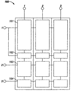
illustrated
herein in terms of the positive voltage regime, in certain embodiments, the
interferometric
modulators can be similarly operated in the negative voltage regime. The row
pulses
decrease in magnitude from left to right, corresponding to the subrows from
top to
bottom. This decreasing magnitude of the pulses is selected to address only
those
modulators in subrows that have smaller actuation and greater release
voltages. For
example, in the illustrated embodiment, potentials of +6 and -6 volts are
applied to the
columns and row pulses of +6, +4, and +2 volts are applied to the rows.
[0081] The pulses of Figure 14 set the state of Row 1 of the display to that
clepicted in Figure 12 as follows. For the first line time for Row 1, Column
1, a Column I
potential of -6 volts is applied along with a row pulse of +6 volts, producing
a 12-volt
difference across the modulators of Row 1, Column 1, to set the state of the
modulators of
each of the Row 1, Column I subrows in the actuated position as illustrated
along the
bottom of Figure 14. The Column 1 potential remains at -6 for the remaining
Row 1 line
times to continue to set the state of each of the elements in the Row 1,
Column 1 subrows
to the actuated position. In Column 2, a Column 2 potential of +6 volts is
applied in
conjunction with the row pulse at +6 volts in the first line time, producing a
zero-volt
difference across the modulators of Row 1, Column 2, to release all modulators
in the
subrows in Row 1, Column 2. During the second line time for Row 1, a Column 2
potential of -6 volts is applied in conjunction with a row pulse of +4 volts,
producing a
10-volt difference across the modulators of Row 1, Column 2, to actuate the
bottom two
subrows of Row 1, Column 2. During the third row time for Row 1, a Column 2
potential
is applied at +6 volts in conjunction with a row pulse of +2 volts, producing
a 4-volt
19
CA 02654185 2008-12-03
WO 2007/145720 PCT/US2007/010499
difference across the modulators of Row 1, Column 2, to release the modulator
in the
bottom subrow of Row 1, Column 2. In Column 3, a Column 3 potential of -6
volts is
applied in conjunction with the row pulse at +6 volts in the first line time,
producing a 12-
volt difference across the modulators of Row 1, Column 3, to actuate all
modulators in the
subrows in Row 1, Column 3. During the second line time for Row 1, a Column 3
potential of +6 volts is applied in conjunction with a row pulse of +4 volts,
producing a 2-
volt difference across the modulators of Row 1, Column 3, to release the
bottom two
subrows of Row 1, Column 3. During the third row time for Row 1, a Column 3
potential
is applied at -6 volts in conjunction with the row pulse of +2 volts,
producing an 8-volt
difference across the modulators of Row 1, Column 3, to actuate the modulator
in the
bottom subrow of Row 1, Column 3.
[0082] Figure 15 is a flowchart illustrating one embodiment of a method 850
of updating an embodiment of a display such as depicted in Figure 12. The
method 850
begins at a block 852 in which the driver 22 of Figure 2 receives image data
value for a
subrow. In one embodiment, the driver 22 receives the data value from a frame
buffer.
Next, at a block 854, the driver 22 applies a row strobe to all subrows of
interferometric
modulators along with a column potential that corresponds to the image data
value.
Moving to block 856, the driver 22 receives the data for the next subrow.
Next, at block
860, the acts of blocks 854 and 856 are repeated for each of the subrows. In
one
embodiment, the acts of the blocks 854 and 856 occur at least partially
concurrently.
[0083] At least one aspect of the present invention is the realization that
quantization artifacts are more visible to the user in low-intensity regions
than in high-
intensity regions because the percentage change between quantization levels is
greater at
lower intensities. For example, in a 7-bit (27 = 128 quantization levels)
system, the
intensity change from level 100 to level 101 is 1%. Most users cannot discern
intensity
changes below about 4%, so transitions at or below this quantization level
appear smooth.
However, the change from level 10 to level 11 is 10%, an intensity change that
is easily
seen by most users. Therefore, at low intensity quantization levels, th'e
quantization of
analog data into discrete digitized quantization steps is clearly seen as an
artifact. The
most straightforward approach to this problem is to digitize at higher bit
densities. For
example, instead of being digitized to 7 bits across the intensity range, the
given signal is
digitized to 10 bits (210 = 1,024 quantization levels) across the intensity
range so that the
analog quantization levels that would have fallen around level 10 in the 128-
level
CA 02654185 2008-12-03
WO 2007/145720 PCT/US2007/010499
configuration fall around level 80 in the 1,024 level configuration. The
transition from
level 80 to level 81 is about 1.2%, and would then be indiscernible to the
user. However,
such increases in system bit density can lead to greater system complexity and
cost (e.g.,
the number of driver connections would increase by about 38% from 24 in a 3x3
7-bit
grayscale display to 33 in a 3x3 10-bit grayscale display).
100841 In interferometric modulator-based systems, these complexity issues
tend to impact the cost and complexity of driver integrated circuits and the
cost and
complexity of the systems themselves. Several drive scheme methods for complex
interferometric modulator displays have been disclosed that reduced driver
complexity
and cost at the expense of imposing even further operational limitations and
tighter
manufacturing tolerances on the interferometric modulator systems. Many of
these drive
schemes also involve adding additional addressing cycles to the
interferometric
modulator. These additional cycles tend to reduce the maximum frame height and
rate
capability of the interferometric modulator or require further technology
development of
the interferometric modulator in order to maintain the frame rate of previous
levels.
Many of these solutions and improvements are overkill in the sense that they
decrease the
quantization step size throughout the entire range of the digitized signal,
even though
there is no need to decrease the step size at the high-intensity end of the
signal range (e.g.,
at least above the quantization steps from about 30 to 31, which is only
3.3%).
[0085] Figure 16 is a schematic diagram of an embodiment of a color
interferometric modulator pixel 160. In the embodiment illustrated in Figure
16, the
interferometric modulator 101 of Figure 10 has been partitioned or replaced by
two
interferometric modulators 161, 162 (or "display elements") arranged in two
subrows that
are configured to communicate with a common row conduit. In Figure 10, the
modulator
101 subtends about 4/7 of the area of the first column. When partitioned as in
Figure 16,
the modulator 161 subtends about half (7/14) of the first column and the
modulator 162
subtends about 1/14 of the first column. The first display element 161 has a
first optically
active area and the second display element 162 has a second optically active
area. In
certain embodiments, the ratio of the first optically active area to the
second optically
active area is approximately equal to an integer to one (e.g., 7 to 1, 7:1,
7/1). In some
embodiments, the integer is 2, 3, 4, 5, 6, 7, 8, 9, or 10. In some
embodiments, the integer
is 3, 7, 15, 31, 63, 127, 255, or any number 2 -l where n is an integer
greater than or
equal to 2.
21
CA 02654185 2008-12-03
WO 2007/145720 PCT/US2007/010499
[0086] When both of the modulators 161, 162 are driven together, the function
of the pixel 160 is unchanged from the pixel 100 schematically depicted in
Figure 10.
Although Figure 16 represents an embodiment partitioning the modulators 101,
104, and
107 in Figure 10, such partitioning may also be appropriate for grayscale
displays (e.g., by
partitioning the modulator 91 depicted in Figure 9).
[0087] As used herein, the terms "divided," "partitioned," and "replaced" in
relation to the plurality of interferometric modulators or mirrors of various
embodiinents
does not require that a larger interferometric modulator or mirror actually be
created and
then partitioned into smaller interferometric modulators or mirrors. Instead,
the terms are
used to compare the relative structures from previously described
configurations. For
example, the modulators 161 and 162 in Figure 16 are typically formed
independently
from one another, as opposed to having been formed as a single modulator 101
as
depicted in Figure 10 and then partitioned into smaller modulators. Moreover,
independent creation is preferable in some embodiments to allow for individual
adjustment of the hysteresis curves for the modulators 161, 162 as described
above.
[0088] Figure 17 is a diagram of modulator position versus applied positive
voltage illustrating one exemplary embodiment of two interferometric
modulators (e.g.,
the two modulators 161, 162 illustrated in Figure 16) that have hysteresis
curve stability
windows in which the actuation voltages are different, but the release
voltages are about
the same. The traces 810 represent the hysteresis loop of the modulator 161
and the traces
808 represent the hysteresis loop of the modulator 162. In certain
embodiments, the
release voltages of the two modulators 161, 162 are considered to be
substantially equal to
one another when any differences between the respective release voltages are
not used to
selectively release one of the modulators and not the other. The hysteresis
loop depicted
by the traces 808 has an actuation voltage of about 9 volts and a release
voltage of about I
volt. The hysteresis loop represented by the traces 810 has an actuation
voltage of about
15 volts and has a release voltage of about 1 volt. Because the release
voltages of the
hysteresis loops of Figure 17 are not exploitably different from each other
(i.e., there are
no voltages that can be applied to reliably release one modulator and not the
other
modulator), the hysteresis loops of Figure 17 cannot be said to be "nested" as
defined
herein.
[0089] Figure 18 is a diagram of modulator position versus applied positive
voltage illustrating another exemplary embodiment of two interferometric
modulators
22
CA 02654185 2008-12-03
WO 2007/145720 PCT/US2007/010499
(e.g., the two modulators 161, 162 illustrated in Figure 16) that have
different stability
windows in which the release voltages are different, but the actuation
voltages are about
the same. The traces 814 represent the hysteresis loop of the modulator 161
and the traces
812 represent the hysteresis loop of the modulator 162. In certain
embodiments, the
actuation voltages of the two modulators 161, 162 are considered to be
substantially equal
to one another when any differences between the respective actuation voltages
are not
used to selectively actuate one of the modulators and not the other modulator.
The
hysteresis loop depicted by the traces 812 has an actuation voltage of about
15 volts and a
release voltage of about 6 volts. The hysteresis loop represented by the
traces 814 has an
actuation voltage of about 15 volts, but has a release voltage of about 1
volt. Because the
actuation voltages of the hysteresis loops of Figure 18 are not exploitably
different from
each other (i.e., there are no voltages that can be applied to reliably
actuate one modulator
and not the other modulator), these hysteresis loops cannot be said to be
"nested" as
defined herein.
[0090] Unlike the embodiment described above in which nested hysteresis
windows are intended to be used to both selectively actuate and selectively
release the
modulators at different voltages, the exemplary embodiments depicted in
Figures 16-18
provide additional manufacturing advantages. The actuation voltages and
release voltages
of each of the nested hysteresis loops of Figure 13 are proximate to each
other. For
example, the release voltage for the loop 804 is about 2 volts and the release
voltage for
the loop 802 is about 4 volts. Thus, in order to selectively release the
modulator
represented by loop 802, but to selectively not release the modulator
represented by loop
804, the voltage applied would be between 2 and 4 volts, preferably around 3
volts. This
voltage accuracy can present problems if the manufacturing tolerances of the
modulators
that release at 2 volts and 4 volts are not sufficiently precise. For example,
if the
modulator represented by loop 802 was manufactured such that its release
voltage was 3.5
volts and the modulator represented by loop 804 was manufactured such that its
release
voltage was 2.5 volts, the tolerance window for the applied voltage would
shrink
considerably. The applied voltage may also vary with manufacturing tolerances
such that
an application of 3 volts to the modulator may actually result in a voltage
difference
across the modulator closer to 2.5 volts. Thus, a voltage applied to the
modulators to
release the modulator represented by loop 802 may inadvertently also release
the
modulator represented by loop 804. The manufacturing tolerances for each of
the three
23
CA 02654185 2008-12-03
WO 2007/145720 PCT/US2007/010499
subrows represented in Figure 13 would need to be highly accurate as there are
six precise
actuation and release voltages that would need to be achieved in order to
accurately
differentially actuate and release each of the three modulators. By contrast,
the two
modulators represented by the hysteresis loops in Figure 17 or Figure 18
require only
three voltages, represented by lines A, B, and C, to differentially actuate
and release the
two modulators. Additionally, because the size differential between the
modulator 161
and the modulator 162 is large, the voltages for actuation and/or release can
advantageously be less precise than the voltages for the configuration
depicted in Figure
13.
100911 Figure 19 schematically illustrates the quantization levels provided by
the schematic of Figure 10. None of the modulators are in the "on" state in
level 0 and all
of the modulators are in the "on" state in level 7. Some of the modulators are
in the "ori"
state in levels 1 through 6, providing varying amounts of intensity. The bit
density at low
intensity ranges is the same as the bit density at high intensity ranges. For
example, as
shown in Figure 20 for the pixel 100 of Figure 10, the intensity difference
between
sequential quantization steps for intensities below level 4 (e.g., intensity
difference of
one) is the same as the intensity difference between sequential quantization
steps for
intensities above level 4 (e.g., intensity difference of one).
[0092] The two modulators 161, 162 of Figure 16 having the hysteresis curves
810, 808 of Figure 17 are used in certain embodiments to provide a higher bit
density at
lower intensity ranges than at higher intensity ranges. For example, in the
sequence of
levels 0 through 7 that can be provided by each column (e.g., as depicted in
Figure 20),
the modulator 161 is actuated or placed in an "on" state only for levels 4 and
above.
Thus, for all quantization steps below level 4, the actuation drive voltage on
the
modulators 161, 162 can be reduced so that only the modulator 162 is
selectively
actuated. Since this modulator 162 has a mirror with preferably about one-half
the optical
weight of the mirror of the modulator 164, the modulators 162, 164, and 163
have weights
in the ratio 1:2:4, respectively, and can be used to generate eight
quantization steps below
quantization level 4, as illustrated in Figure 21. The quantization steps
below level 4 are
illustrated in Figure 22. Similarly, the two modulators 161, 162 of Figure 16
having the
hysteresis curves 814, 812 of Figure 18 are used in certain other embodiments
to provide
a higher bit density at lower intensity ranges than at higher intensity
ranges.
24
CA 02654185 2008-12-03
WO 2007/145720 PCT/US2007/010499
[0093] Referring again to Figure 16, when the mirrors 164, 163, 162, 161
subtend the pixel in a ratio of 2:4:1:7, respectively, the number of
sequential quantization
steps are more than doubled in the lower portion of the display intensity
range, which is
the portion of the quantization range most in need of finer quantization. For
example,
comparing Figures 20 and 22, the number of sequential quantization steps for
intensities
below level 4 (i.e., eight) in Figure 22 is more than double the number of
sequential
quantization steps for intensities above level 4 (i.e., three) in either
Figure 20 or Figure
22. That is, rather than actuating and releasing three modulators to achieve
seven
quantization steps, four of which are below the fourth quantization level, as
depicted in
Figures 19 and 20, four modulators are actuated and released to provide eleven
quantization steps, eight of which are below the fourth quantization level, as
depicted in
Figures 21 and 22. As used herein, the term "quantization step" refers to the
change from
one amount of intensity to the next amount of intensity and the term
"quantization level"
refers to the change from one bit depth to the next bit depth. For example,
the change in
intensity from one modulator to the next in the top row of Figure 21 is a
quantization step,
but not a quantization level, while the change in intensity from one modulator
to the next
modulator in the bottom row of Figure 21 is both a quantization step and a
quantization
level. It will be appreciated that the effect is much more pronounced at bit
depths greater
than 3-bit.
[0094] Figure 23 is a schematic diagram of an embodiment of a color
interferometric modulator pixel 230. Although Figure 23 represents an
embodiment
partitioning the modulators 102, 105, and 108 in Figure 10, such partitioning
may also be
appropriate for grayscale displays (e.g., by partitioning the modulator 92
depicted in
Figure 9). In the embodiment illustrated in Figure 23, the modulator 104 has
been divided
into two modulators 232, 233 (or "display elements") arranged in subrows that
are
configured to communicate with a common row conduit. In Figure 10, the
modulator 102
subtends about 2/7 of the area of the first column. When partitioned as in
Figure 23, the
modulator 232 subtends about 3/14 of the first column and the modulator 233
subtends
about 1/14 of the first column. When both of the modulators 232, 233 are
driven
together, the function of the pixel 200 is unchanged from the pixel 100
schematically
depicted in Figure 10. The hysteresis loops for the modulators 232, 233 may
share a
common actuation voltage or'a common release voltage as displayed in Figures
17 and
18.
CA 02654185 2008-12-03
WO 2007/145720 PCT/US2007/010499
[0095] When the modulators 234, 233, 232, 231 subtend the pixel in a ratio of
2:1:3:8, respectively, the number of sequential, quantization steps (i.e.,
two) are doubled
below level 2 of the display quantization range, which is part of the portion
of the
quantization range most in need of finer quantization. Rather than actuating
and releasing
four modulators to provide eleven quantization steps, eight of which are below
the fourth
quantization level, as depicted in Figures 21 and 22, four modulators are
actuated and
released to provide eleven quantization steps, six of which are below the
fourth
quantization level, as depicted in Figures 24 and 25. Because the schematic
illustrated in
Figure 16 provides finer quantization steps between level 2 and level 4,
partitioning the
mirror 101 of Figure 10 is preferred to partitioning the mirror 104 of Figure
10.
[0096] Even finer quantization may be created by partitioning both the mirror
101 and the mirror 104 depicted in Figure 10, as illustrated by the schematic
diagram in
Figure 26. As shown by Figures 27 and 28, such a schematic results in 17
quantization
steps, 12 of which are below the fourth quantization level. For another
example of the
difference between a "quantization step" and a "quantization level, the change
in intensity
from the second modulator from the left in the top row of Figure 27 to the
third modulator
from the left in the top row of Figure 27 is a quantization step, while the
change in
intensity from the first modulator from the left in the top row of Figure 27
to the fifth
modulator from the left in the top row of Figure 27 is a quantization level.
(0097] Still finer quantization may be achieved by partitioning all three
mirrors 101, 104, and 107 in Figure 10, as illustrated by the schematic
diagram in Figure
29. As shown by Figure 30, such a configuration results in 26 quantization
steps, 18 of
which are below the fourth quantization level. Thus, while maintaining only
six total
leads to a color pixel, the number of quantization steps advantageously
increases from 7
to 26, most of which are in the region of low intensity most in need of finer
quantization.
This configuration dramatically reduces quantization level spacing at low
intensities, the
display range where it is most needed, without increasing the number of
address lines
from the driver IC.
[0098] Various specific embodiments have been described above. Although
the invention has been described with reference to these specific embodiments,
the
descriptions are intended to be illustrative of the invention and are not
intended to be
limiting. Various modifications and applications may occur to those skilled in
the art
without departing from the true scope of the invention as defined in the
appended claims.
26