Note: Descriptions are shown in the official language in which they were submitted.
CA 02654216 2008-12-02
-1-
DESCRIPTION
Resistor, particularly an SMD resistor, and associated production method
The invention relates to a resistor, in particular an SMD resistor, and a
corresponding production method according to the coordinated claims.
Figure 4 shows an exemplary embodiment of a conventional SMD (Surface
Mounted Device) resistor 1, which is marketed by the applicant and which in a
similar form is described, for example, in DE 43 39 551 Cl. The known SMD
resistor 1 comprises a planar metallic substrate 2, which may be composed of
copper, for example. In the production process an electrically insulating
adhesive
layer 3 is applied to the upper side of the substrate 2, and then serves to
bond a
resistive film to the upper side of the substrate 2. The resistive film is
then
structured by an etching process, so that a meandering resistance path 4 is
formed on the upper side of the substrate 2. The resistor 1 is then covered by
a
protective lacquer 5, which electrically insulates the resistance path 4.
Before
completion, a transverse incision 6 is then made in the substrate 2, which
divides
the substrate 2 into two separate support elements 2.1, 2.2, thereby
preventing a
direct flow of current between the two support elements 2.1, 2.2. The support
elements 2.1, 2.2 therefore here form the electrical connection parts of the
SMD
resistor 1, which can be soldered onto solder pads 7, 8, as is indicated
schematically by the arrows in the drawing.
A disadvantage to the known SMD resistor 1 is the intricate electrical
connection
of the underlying support elements 2.1, 2.2 to the resistive film bonded on
top,
which forms the resistance path 4. For this purpose a conductive surface must
first
be achieved in preparation for a current-carrying, electroplated contact on
the
outer edge of the adhesive layer 3 (chemical through-hole plating), before
then in
a multistage electroplating process applying a layer of copper, which will
reliably
conduct the total current. This contact, however, is part of the current path
through
the SMD resistor and therefore also has an influence on the resistance of the
SMD
resistor 1, which in the case of low impedances with a resistance of less than
25mQ means that the resistance has to be adjusted on the separated individual
SMD resistor 1, a resistance adjustment on a blank with multiple resistors in
this
CA 02654216 2008-12-02
-2-
case being precluded.
A further disadvantage of the known SMD resistor 1 stems from the incision 6
in
the substrate 2, since the incision 6, for mechanical stabilizing of the SMD
resistor
1, is filled with a lacquer or epoxy resin, which expands during the soldering-
on
process and leads to bending of the SMD resistor 1, the bending being
virtually
frozen in once the solder has solidified, and at very least leaving a visible
defect in
the finished component. This problem occurs particularly with the use of lead-
free
solders, which require a higher soldering temperature. In addition, a certain
volume of lacquer is needed in the incision 6, in order to mechanically
stabilize the
SMD resistor 1 despite the presence of the incision 6, which in turn implies
that the
substrate 2 is relatively thick. In practice, the substrate 2 must therefore
have a
thickness of at least 0.5mm, which places limits on the miniaturisation of the
SMD
resistor 1. Regardless of the thickness of the substrate 2, the mechanical
load-
bearing capacity of the SMD resistor 1 is limited by virtue of the mechanical
weakening introduced by the incision 6.
A further disadvantage of the SMD resistor 1 results from the high
electroplating
costs, which account for approximately 25% of the total production costs.
These
high electropiating costs stem from the fact that the lateral contact of the
two
support elements 2.1, 2.2 to the resistance path 4 must carry the full current
flow,
so that the demands placed on the density and the effective cross section of
the
electroplated copper layer are relatively high. In addition, at low-impedance
resistance values the influence of the copper on the electrical
characteristics is not
entirely negligible.
Finally the support elements 2.1, 2.2 as connection parts do not conform to
the
usual standard dimensions of solder pads, but are substantially greater in
length.
Any shortening of the two support elements 2.1, 2.2 and hence a widening of
the
incision 6, however, would lead to a further mechanical and thermal weakening
and is therefore not possible.
Figure 5 shows another type of a known SMD resistor 9, which is marketed by
the
applicant, a similar type also being described in EP 0 929 083 B1. The SMD
resistor 9 comprises a planar, thin aluminium substrate 10, the substrate 10
in this
CA 02654216 2008-12-02
-3-
type having no incision and hence no mechanical weakening. Bonded to the
underside of the planar substrate 10 by an adhesive layer 11 is a resistive
film 12,
which is structured by an etching process and forms a meandering resistance
path. Lamellar copper contacts 13 are applied to the underside on the narrow
end
sides of the SMD resistor 9, and form electrical contacts with lamellar
connection
parts 14, 15. Finally, the SMD resistor 9 of this type has a protective
lacquer
coating 16, 17 on the upper side and on the underside.
Of advantage in this type of the SMD resistor 9 is firstly the fact that the
substrate
has no mechanical weakening, so that the ensuing problems described above
10 are avoided.
A disadvantage of the SMD resistor 9, however, is the fact that the connection
parts 14, 15 and hence also the soldering points are situated on the underside
of
the SMD resistor 9, where the soldering points are not open to visual
inspection.
Attaching soldering points laterally is not possible in the case of the SMD
resistor
9, however, since the soldering points would otherwise create an unwanted
electrical shunt via the electrically conductive substrate 10.
A further disadvantage of the SMD resistor 9 is that the substrate 10 of
anodized
aluminium is relatively hard, which means that when separating the SMD
resistor 9
by sawing, the life of the saw blade is reduced. In addition, sawing off the
individual SMD resistors 9 from an aluminium blank leads to an unwanted saw
burr on the sawn-off SMD resistor 9, owing to the low melting point of the
aluminium compared to copper.
Finally, applying the protective lacquer 6 to the upper side of the SMD
resistor 9
and the inscription of the SMD resistor 9 leads to material-based production
problems.
Another conventional type of SMD resistor finally comprises a planar ceramic
substrate, which on its upper side carries a structured resistive film, the
resistive
film likewise forming a meandering resistance path. The electrical contact of
the
SMD resistor is here achieved by solder caps of a highly conductive, generally
electroplate-reinforced, solderable metallic layer (for example nickel-
chromium
alloy), the solder caps being of U-shaped cross section and enclosing the
CA 02654216 2008-12-02
-4-
opposing narrow edges of the SMD resistor with a cap shape. The solder caps
are
here laterally accessible, so that when soldering up laterally visible
soldering
points are produced, which facilitate visual inspection of the soldered
connections.
A disadvantage with this type, however, is the fact that the substrate is
composed
of ceramic and therefore has a relatively low thermal conductivity compared to
copper (cf. Fig. 4) or aluminium (cf. Fig. 5) and a low coefficient of thermal
expansion poorly suited to a normal circuit board. In addition, the resistive
film is
here located on the upper side of the substrate, which has the detrimental
influences on the overall resistance previously described.
Similar resistors having a non-metallic support element are disclosed in US
2004/0252009 Al and DE 30 27 122 Al, for example.
Finally, DE 196 46 441 Al discloses a resistor, in which the connection parts,
however, are attached solely to the underside, so that no visual inspection of
the
soldered connection is possible.
Proceeding from the known SMD resistor 9 according to Fig. 5, the object of
the
invention, therefore, is to eliminate the disadvantages of the SMD resistor 9,
by
facilitating visual inspection of the soldering points.
This object is achieved by a resistor according to the invention and a
production
method according to the invention, as specified in the coordinated claims.
The invention embraces the general technical teaching of arranging the
connection parts on the resistor laterally exposed, so that the connection
parts can
be wetted by a solder in manner that is visible, in order to allow a visual
inspection
of the respective soldered connection.
The resistor according to the invention is preferably embodied as an SMD
resistor
and allows a conventional surface mounting. The invention is not confined to
SMD
resistors, however, but in principle also encompasses other types of resistors
which, for example, provide for a conventional contact by solder pins.
The resistor according to the invention furthermore comprises a plane metallic
support element, which due to the composition of its metallic material has a
good
CA 02654216 2008-12-02
-5-
thermal conductivity and a suitable coefficient of thermal expansion, which is
advantageous in the operation of the resistor according to the invention.
In addition the resistor according to the invention has a plane resistance
element
composed of a resistive material, the resistance element being located on the
underside of the plane support element.
The term `a plane resistance element or support element' used in the context
of
the invention is to be interpreted in general terms and is not confined to the
mathematical or geometric definition of a plane surface. This feature is
preferably
intended to imply, however, that the lateral extent of the support element or
the
resistance element is substantially greater than the thickness of the support
element or resistance element. In addition, this feature also preferably
embraces
the idea that the upper side and the underside of the support element or
resistance element in each case run parallel to one another. The support
element
and the resistance element are furthermore preferably plane, although, curved
or
arched shapes of the support element and the resistance element are also
possible.
In addition, the resistor according to the invention comprises at least two
separate
metallic connection parts, which form the electrical contacts of the
resistance
element and are partially located on the underside of the support element. In
contrast to the known SMD resistor according to Fig. 5 described in the
introductory part, however, the connection parts are not located entirely on
the
underside, but are at least in part exposed at the side of the resistor, so
that when
soldering up laterally visible soldering points are formed, which facilitate
visual
inspection.
The metallic connection parts preferably each extend laterally on the resistor
upwards to the metallic support element, where the connection parts touch and
come into electrical and thermal contact with the support element. For
example,
the connection parts may each have a U-shaped cross section and each enclose
the resistor on opposite edges in a cap shape, a lateral metal coating in the
contact area also being possible.
In the resistor according to the invention, however, the metallic support
element
CA 02654216 2008-12-02
-6-
only serves as a substrate and as a thermal conductor, the support element in
the
resistor according to the invention not being intended to serve as an
electrical
conductor, in order to avoid unwanted shunts via the metallic support element.
The
metallic support element in the resistor according to the invention therefore
preferably has an incision, which divides the support element into at least
two
parts electrically isolated from one another, and prevents a flow of current
between
the two connection parts via the support element. In its simplest form the
incision
may be embodied in the same way as in the known SMD resistor according to Fig.
4, in which the resistive film, however, is located on the upper side of the
substrate. The incision in the support element, however, preferably runs at
least
partially slanting, for example in a V-shape, a W-shape or in a meandering
shape.
Such a design shape of the incision in the support element advantageously
leads
to a greater mechanical stability of the resistor than is the case with a
transverse
incision.
The connection parts in the resistor according to the invention are
furthermore
preferably of a size adapted to suit standard solder pads, so that the
resistor
according to the invention differs from the known SMD resistor according to
Fig. 4,
in which the connection parts have a substantially greater lateral extent. In
the
resistor according to the invention the connection parts therefore preferably
have a
lateral extent, which is less than 30%, 20% or 15% of the distance between the
two connection parts. In the case of an extreme miniaturisation of the
resistor
according to the invention, a dimensioning of the connection parts relative to
the
distance between the connection parts on the other hand leads to excessively
small connection parts. Limits of 1 mm, 0.5mm or 0.1 mm can then be defined as
maximum values for the lateral extent of the connection parts. For example,
the
lamellar connection parts may have a width ranging from 0.1-0.3mm (type 0402),
0.15-0.40mm (type 0603), 0.25-0.75mm (type 1206) or 0.35-0.85mm (type 2512).
The resistive material of the resistor according to the invention is
preferably
composed of a copper-manganese alloy, such as a copper-manganese-nickel
alloy, for example. For example, the alloys CuMn12Ni, CuMn7Sn or CuMn3 may
be used as resistive material. Alternatively it is also possible, within the
scope of
the invention, to use a nickel-chromium alloy, in particular a nickel-chromium-
CA 02654216 2008-12-02
-7-
aluminium alloy as resistive material. Examples of such possible alloys are
NiCr20AlSilMnFe, NiCr6015, NiCr8020 and NiCr302O. In addition, the resistance
element may also be composed of a copper-nickel alloy, such as CuNi15 or
CuNi10, for example. In the resistive material that can be used, however, the
invention is not limited to the examples cited above, other resistive
materials also
in principle being feasible.
It should further be mentioned that the resistor according to the invention
preferably has a high degree of miniaturisation. For example, the thickness of
the
resistor according to the invention may be less than 2mm, 1 mm, 0.5mm or even
0.3mm. The length of the resistor according to the invention may be less than
10mm, 5mm, 2mm or even less than 1 mm. The width of the resistor according to
the invention on the other hand is preferably less than 5mm, 2mm or even less
than 1 mm.
Accordingly, the support element in the resistor according to the invention
preferably has a thickness ranging from 0.05-0.3mm.
It should further be mentioned that the resistor on its outside is preferably
coated
with a temperature-resistant insulation layer (hereinafter generally referred
to as
solder resist), which is familiar from conventional SMD resistors. The solder
resist
in the resistor according to the invention is therefore preferably applied to
the
upper side of the support element and to the underside of the resistance
element.
In addition it should be mentioned that the connection parts are preferably
composed of a highly conductive material, in order to achieve the smallest
possible connection resistance. The support element and/or the connection
parts
in the resistor according to the invention are furthermore preferably composed
of a
thermally highly conductive material, in order to achieve an efficient heat
dissipation from the resistance element, for example. The connection parts
and/or
the support element may for this purpose be composed of copper or a copper
alloy, for example.
The individual connection parts are preferably cap-shaped and may be of U-
shaped cross section, for example. In such a cap-shaped connection part having
a
U-shaped cross section, the upper leg of the connection part encloses the
support
CA 02654216 2008-12-02
-8-
element at the top, whilst the lower leg of the U-shaped connection part
encloses
the resistance element at the bottom. In such a cap-shaped connection part the
cap-shaped connection part is preferably intended to enclose the support
element
and/or the resistance element not only at top and bottom but also laterally.
This is
possible if the cap-shaped connection parts are applied only when the
resistors
are parted from the blank in the course of the production process according to
the
invention, since only then are the lateral cut faces of the detached resistors
exposed.
It should further be mentioned, that even in the resistor according to the
invention
an adhesive layer is preferably located between the plane resistance element
and
the plane support element. For one thing, the adhesive layer fixes the plane
resistance element to the underside of the support element. For another, the
adhesive layer is electrically insulating and therefore prevents unwanted
electrical
shunts via the metallic support element.
The plane resistance element in the resistor according to the invention is
furthermore preferably structured by an etching process or in some other way
(for
example by laser machining), so that the resistance element has a simple
rectangular or meandering resistance path, as is also the case with the known
SMD resistors described in the introductory part.
The resistor according to the invention allows advantageously low resistances
in
the milliohm range, in which the resistance may be less than 500mS2, 200mQ,
50mS2, 30mS2, 20m4, IOmS2, 5mS2 or even less than 1 mS2.
It should further be mentioned that the resistance element in the resistor
according
to the invention preferably affords complete external electrical insulation,
apart
from the connection parts.
However, the invention encompasses not only the resistor according to the
invention described above but also a corresponding production method, in which
the connection parts are attached to the resistor so that the connection parts
are
laterally exposed and can be wetted by a solder in a manner that is visible,
in
order to allow a visual inspection of the respective soldering point.
CA 02654216 2008-12-02
-9-
In the production method according to the invention the incision in the
metallic
support element described above can be made, for example, by an etching
process or by laser machining.
The same applies to the structuring of the resistance element to form the
meandering resistance path, which can likewise be made by an etching process
or
by laser machining.
It should further be mentioned with regard to the production method according
to
the invention that the resistors can be separated from a blank by sawing, by
punching or by laser cutting. In producing the support elements from copper,
the
invention advantageously allows a longer service life of the saw blade used,
since
copper is substantially softer than the anodized aluminium used in the known
SMD
resistor according to Fig. 5, described in the introductory part.
In addition the invention advantageously allows a resistance adjustment to be
carried out on a blank with multiple resistors not yet separated, so that
after
separation of the resistors no further resistance adjustment is necessary.
Other advantageous developments of the invention are characterized in the
dependent claims or are explained in more detail below together with the
description of the preferred exemplary embodiments of the invention, with
reference to the drawings, in which:
Fig. 1 shows a perspective view of an SMD resistor according to the
invention,
Figs. 2A-2G show various stages in the production of an SMD resistor according
to the invention,
Fig. 3 shows the production method according to the invention in form of a
flow chart,
Fig. 4 shows a perspective of the known SMD resistor described in the
introductory part, and
Fig. 5 shows a perspective view of the SMD resistor likewise described in
CA 02654216 2008-12-02
-10-
the introductory part.
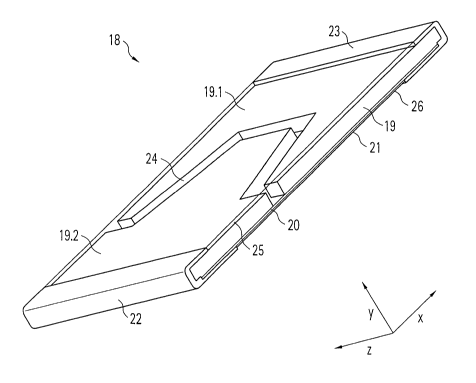
The cross sectional view in Fig. 1 shows an SMD resistor 18 according to the
invention, which may be of type 0604, for example. This means that the SMD
resistor 18 has a length in the X direction of 0.06 inches (1.524mm) and a
width in
the Z direction of von 0.04 inches (1.016mm). The SMD resistor 18 may
furthermore have a thickness in the Y direction of 0.4mm, for example.
The SMD resistor 18 has a planar support element 19 made of copper, a
resistive
film 21 of a copper-manganese-nickel alloy (CuMn12Ni) being adhesively bonded
to the underside of the support element 19 by means of an adhesive layer 20.
For
one thing, the adhesive layer 20 produces a fixing of the resistive film 21 on
the
underside of the planar support element 19. For another, the adhesive layer 20
is
electrically insulating and therefore insulates the conductive support element
19
from the resistive film 21.
The SMD resistor 18 furthermore has cap-shaped connection parts 22, 23 on
either side, the two connection parts 22, 23 enclosing the support element 19
and
the resistive film 21 at the top, sides and bottom. The two connection parts
22, 23
therefore electrically bond the resistive film 21, so that in the assembled
state a
current can flow via the two connection parts 22, 23 and the resistive film
21.
In the planar support element 19 is a substantially V-shaped incision 24,
which
divides the support element 19 into two parts 19.1, 19.2, the two parts 19.1,
19.2
being electrically isolated from one another by the incision 24. In
conjunction with
the incision 24, the adhesive layer 20 between the resistive film 21 and the
planar
support element 19 therefore prevents unwanted electrical shunts via the
support
element 19. The support element 19 therefore here serves solely as mechanical
substrate and to dissipate heat, but not to conduct current.
Finally, it should also be mentioned that a solder resist 25 is applied to the
upper
side of the support element 19 and extending between the two connection parts
22, 23. In addition, a solder resist 26 is also applied to the underside of
the
resistive film 21 and extending between the two connection parts 22, 23. In
the
SMD resistor 18 the resistive film 21 is therefore completely insulated
externally
except for the connection parts 22, 23.
CA 02654216 2008-12-02
-11-
The production method according to the invention will now be described below
with reference to Figs. 2A-2G and to the flow chart in Fig. 3, Figs. 2A-2G
showing
various intermediate stages of the SMD resistor 18 according to the invention.
In a first step S1 of the production method according to the invention the
support
element 19 in the form of a copper-foil is first prepared, as is shown in Fig.
2A.
In a further step S2 the resistive film 21 is then adhesively bonded onto the
underside of the support element 19, the bonding being achieved by means of
the
adhesive layer 20, as can be seen from Fig. 2B.
In the next step S3 the incision 24 is then made in the support element 19, in
order
to prevent any subsequent electrical shunt via the electrically conductive
support
element 19. The incision 24 can be produced by an etching process or by laser
machining, for example. The step S3 leads to the intermediate stage according
to
Fig. 2C.
In step S4 a solder resist is then applied to the upper side of the support
element
19, in a manner known in the art.
In a further step S5 an etched structure is then introduced into the resistive
film 21,
which then subsequently forms a meandering resistance path.
In step S6 the solder resist 26 is then applied to the underside of the
resistive film
21, as can be seen from Fig. 2D.
In the next steps S7 and S8 there then follows a lamellar exposure of the
support
element 19 at the opposite edges of the SMD resistor 18 in the X-direction, in
order that the connection parts 22, 23 can then come into thermal contact with
the
support element 19. The cross sectional view in Fig. 2E shows this state after
the
lamellar exposure of the support element.
In step S9 a copper layer with a thickness of 10 m, for example, is then
applied to
the exposed edges of the resistive film 21 on the underside thereof.
In the next step S10 a resistance adjustment is then performed on a blank with
numerous SMD resistors not yet separated.
CA 02654216 2008-12-02
-12-
Following the individual resistance adjustment, the SMD resistors are then
parted
from the blank in step S11, which may be done by sawing, punching or by laser
machining.
In a final step S12 the connection parts 22, 23 are then applied as solder
caps to
the exposed edges. Applying the connection parts 22, 23 in this way after
separating the SMD resistor 18 allows the connection parts 22, 23 to also
enclose
the support element 19 laterally at the cut faces, as can be seen from the
perspective view in Fig. 1.
Fig. 2G finally shows the SMD resistor 18 according to the invention on a
circuit
board 27 with two standard solder pads 28, 29 and two soldering points 30, 31.
It
can be seen from the cross sectional view that the soldering points 30, 31 are
exposed at the sides of the SMD resistor 18 and are therefore open to visual
inspection.
The invention is not limited to the preferred exemplary embodiments described
above, a number of variants and modifications instead being possible, which
also
make use of the idea of the invention and therefore come within the scope of
the
patent.
CA 02654216 2008-12-02
List of reference numerals
1 SMD resistor
2 substrate
2.1, 2.2 support elements
3 adhesive layer
4 resistance path
5 protective lacquer
6 incision
7 solder pad
8 solder pad
9 SMD resistor
10 substrate
11 adhesive layer
12 resistive film
13 copper contacts
14, 15 connection parts
16, 17 protective lacquer coat
18 SMD resistor
19 support element
19.1, 19.2 parts
20 adhesive layer
21 resistive film
22, 23 connection parts
24 incision
25, 26 solder resist
27 circuit board
28, 29 standard solder pads
30, 31 soldering points
*****