Note: Descriptions are shown in the official language in which they were submitted.
CA 02654412 2012-03-20
SYSTEM AND METHOD FOR COMMUNICATING POWER SYSTEM
INFORMATION THROUGH A RADIO FREQUENCY DEVICE
Inventors: Edmund 0. Schweitzer, HI, Witold R. Teller, Mark 3, Bosold, Douglas
A. Park, Laurence Virgil Feight, Steven A. McMahon,
James R, Kesler, Luther S. Anderson, Donald C. Hicks
Field of the Invention
[002] The present invention relates generally to a system and method for
communicating power system information, and more particularly to a system and
method for communicating power system information through a radio frequency
device.
Description of the Prior Art
[003] Power transmission and distribution systems may include power system
protection, monitoring, and control devices such as sensors, protective
relays,
faulted circuit indicators, and the like. Throughout, the term
1
CA 02654412 2008-11-19
WO 2007/137205 PCT/US2007/069312
"power system device" will include any power system protection, monitoring,
or control device. Detection devices are used in the power system industry to
monitor certain areas and conditions in the power system. Some examples
of detection devices include: faulted circuit indicators (FCIs); water, high
voltage electric field, specific gravity, light, and sound sensors; gas
sensors
such as CO, C02, SOx, NOx, Ammonia, Arsine, Bromine, Chlorine, Chlorine
Dioxide, VOCs, Combustibles, Diborane, Ethylene Oxide, Fluorine,
Formaldehyde, Germane, Hydrogen, Hydrogen Chloride, Hydrogen Cyanide,
Hydrogen Fluoride, Hydrogen Selenide, Hydrogen Sulfide, Oxygen, Ozone,
Methane, Phosgene, Phosphine, Silane, and the like; pressure sensors for
sensing, for example, pressure in a gas line, water line, waste line, oil
line,
and the like; temperature sensors; electromagnetic radiation sensors;
radiation sensors; smoke sensors; particulate matter sensors; liquid phase
sensors such as pH, turbidity, Br-, Ca2+, Cl-, CN-, Cu2+, F-, I-, K+, Na+,
NH4+, N03-, Pb2+, S-(AG+), conductivity sensors, and the like; radio wave
sensors; electrical sensors such as under voltage sensors, over voltage
sensors, under current sensors, over current sensors, frequency sensors
and the like; power factor alarms; demand overload indicators; sensors that
detect the presence of primary system voltage; sensors that determine if a
sealed subsurface fuse has operated by sensing voltage on each side of
fuse element with loss of load current; sensors that sense the open or closed
position of a subsurface switch; voltage sensors which monitors status of
lead-acid batteries used to run controller or motor operators for subsurface
switches; power quality sensors which detect primary voltage swells and
2
CA 02654412 2008-11-19
WO 2007/137205 PCT/US2007/069312
sags along the distribution system, and other sensors that detect power
quality issues and send an alarm status.
[004] Faulted circuit indicators (FCls) play a vital role in detecting and
indicating faults and locations of faulted conductors to decrease the duration
of power outages and improve the reliability of power systems throughout
the world. Electrical utilities depend on faulted circuit indicators to help
their
employees quickly locate faulted conductors. Most conventional faulted
circuit indicators utilize a mechanical target or a light emitting diode (LED)
to
provide a visual indication of a faulted conductor. By visually scanning
faulted circuit indicators located at a site, an electrical utility crew can
quickly
locate a fault. Industry statistics indicate that faulted circuit indicators
reduce
fault location time by 50% -- 60% versus the use of manual techniques, such
as the "refuse and sectionalize" method. Nonetheless, electrical utilities
still
spend substantial amounts of time and money determining the locations of
faults on their networks.
[005] A recent advancement is the use of Radio Frequency ("RF")
technology within fault circuit indication systems. In one prior art system,
each faulted circuit indicator communicates with a radio interface unit which
communicates the occurrence of a fault to an external receiver. The radio
interface unit is often located in proximity to an FCI within an underground
vault, which is susceptible to external elements. For example, vaults may
often be filled with water thereby exposing the radio interface unit located
therein to also be exposed to such. In another example, for overhead FCI
systems, radio interface units are also exposed to the external elements as
3
CA 02654412 2008-11-19
WO 2007/137205 PCT/US2007/069312
they are situated in proximity to the overhead FCI device.
[006] As such, it is an object of the present invention to provide a system
for
communicating power system information through a radio frequency device
which may endure harsh external elements.
[007] Prior art fault circuit indication systems have further been found to be
insufficient in their reporting of data. In one prior art system, a wireless
device is used to monitor radio signals from RF equipped faulted circuit
indicators that are connected to a radio interface unit. Using a wireless
device, a utility crew can locate a fault and determine when the fault has
been properly cleared by monitoring the display of the wireless device.
However, conventional wireless devices provide no indication as to whether
a particular faulted circuit indicator is actually connected to the radio
interface unit. In addition, prior art devices do not display the status of a
plurality of or multiple groups of faulted circuit indicators simultaneously.
Prior art systems also do not provide the capability to view detection devices
or sensors for communicating other conditions related to the power system.
[008] Accordingly, one object of this invention is to provide a user interface
for a wireless device that simultaneously displays the status of multiple
groups of monitored faulted circuit indicators. Another object of this
invention
is to provide an indication on a wireless device of whether a faulted circuit
indicator is connected to a remote monitoring device, such as a radio
interface unit. Yet another object of the present invention is to provide data
on a wireless device for other conditions related to the power system.
Summary of the Invention
4
CA 02654412 2008-11-19
WO 2007/137205 PCT/US2007/069312
[009] A system for communicating information between a detection device
and a wireless device is provided which is adapted to endure harsh
conditions (e.g., prolonged exposure to water). The system generally
includes a detection device adapted to monitor a condition related to a
power system. A radio interface unit is in communication with the detection
device via a communication member. A wireless device is further provided
which is in radio communication with the radio interface unit such that the
detection device communicates information to the wireless device through a
radio interface unit.
[0010] In an embodiment, the detection device is a power system device
(e.g., a faulted circuit indicator). In another embodiment, either the
communication member or the radio interface unit is substantially self-
contained. In yet another embodiment, the communication member may be
adapted to communicate power system information to the radio interface unit
without either a mechanical or electrical connection therebetween.
[0011] In yet another embodiment, the detection device includes one
selected from the list consisting of devices for detecting: CO, C02, SO,, NON,
Ammonia, Arsine, Bromine, Chlorine, Chlorine Dioxide, volatile organic
compounds, Diborane, Ethylene Oxide, Fluorine, Formaldehyde, Germane,
Hydrogen, Hydrogen Chloride, Hydrogen Cyanide, Hydrogen Fluoride,
Hydrogen Selenide, Hydrogen Sulfide, Oxygen, Ozone, Methane,
Phosgene, Phosphine, Silane, pressure, temperature, electromagnetic
radiation, atomic radiation, smoke, particulate matter, pH, turbidity, Br",
Cat+,
Cl-, CN-, Cue-1, F-, 1-, K+, Na+, NH 4+, N03 Pb2+, S"(AG+), conductivity, over
CA 02654412 2008-11-19
WO 2007/137205 PCT/US2007/069312
voltage, under voltage, over current, under current, frequency, water, high
voltage electric field, specific gravity, light, and sound.
Brief Description of the Drawings
[0012] Although the characteristic features of this invention will be
particularly pointed out in the claims, the invention itself, and the manner
in
which it can be made and used, can be better understood by referring to the
following description taken in connection with the accompanying drawings
forming a part hereof, wherein like reference numerals refer to like parts
throughout the several views and in which:
[0013] FIG. I illustrates a system view of a faulted circuit indicator
monitoring
system in accordance with an aspect of the present invention.
[0014] FIG. 2A illustrates a wireless device communicating with eight radio
interface units, each of which is connected to four groups of faulted circuit
indicators in accordance with an aspect of the present invention.
[0015] FIG. 2B illustrates the underground vault 200e of FIG. 2A.
[0016] FIG. 3 illustrates a circuit diagram of the radio interface unit of
FIG. 1
in accordance with an aspect of the present invention.
[0017] FIG. 4A and 4B illustrate an example of the housing of a radio
interface unit in accordance with an aspect of the present invention.
[0018] FIGS. 5A and 5B illustrate a cross-sectional view of an embodiment of
the present invention system showing the engagement of the communication
member and interface.
6
CA 02654412 2008-11-19
WO 2007/137205 PCT/US2007/069312
[0019] FIG. 5C and 5D illustrate a cross-sectional view of another
embodiment of the present invention system showing the engagement of the
communication member and interface,
[0020] FIG. 6 is a circuit diagram of an embodiment of the present invention
system illustrating the interaction between the communication member and
the interface.
[0021] FIG. 7 is a circuit diagram showing magnetic field interference with
the communication member and the interface.
[0022] FIG. 8 is a circuit diagram of an embodiment of the present invention
system showing the compensation for magnetic field interference
implementing a differential inductor coil configuration.
[0023] FIG. 9 illustrates an example of the housing of a radio interface unit
in
accordance with an aspect of the present invention.
[0024] FIGS. 10A and 10B illustrate a cross-sectional view of an embodiment
of the present invention system showing the engagement of the
communication member and interface implementing a differential inductor
coil configuration.
[0025] FIG. 10C and 10D illustrate a cross-sectional view of another
embodiment of the present invention system showing the engagement of the
communication member and interface implementing a differential inductor
coil configuration.
[0026] FIG. 11 is a circuit diagram of an embodiment of the present invention
system illustrating the interaction between the communication member and
the interface implementing a parallel inductor coil configuration.
7
CA 02654412 2008-11-19
WO 2007/137205 PCT/US2007/069312
[0027] FIG. 12 is a circuit diagram of an embodiment of the present invention
system illustrating the interaction between the communication member and
the interface implementing a serial inductor coil configuration.
[0028] FIG. 13 is a circuit diagram of an embodiment of the present invention
system illustrating the interaction between the communication member and
the interface implementing a circuit for preventing false latching from
ringing
currents.
[0029] FIGS. 14A-14C are graphical representations depicting the
progression of a ringing pulse exiting the detection circuit of FIG. 12 and
the
suppression of false latching caused by ringing.
[0030] FIG. 15 illustrates a dial having a plurality of magnets in a select
arrangement, wherein each arrangement corresponds to a select
identification setting.
[0031] FIGS. 16A-16D are circuit diagrams illustrating various embodiments
of systems for identifying a power system device according to various
aspects of the present invention.
[0032] FIG. 17A illustrates the user interface of a wireless device of FIGS.
2A
and 2B used to scan a number of groups of faulted circuit indicators
connected to separate radio interface units for their status.
[0033] FIG. 17B illustrates the same wireless device user interface of FIG.
17A after a scan operation has been completed.
[0034] FIG. 17C illustrates the same wireless device user interface FIG. 17A
where a number of faulted circuit indicators attached to the selected radio
interface unit are asserting a fault condition.
8
CA 02654412 2008-11-19
WO 2007/137205 PCT/US2007/069312
[0035] FIG. 17D illustrates the same wireless device user interface FIG. 17A
where, in addition to the selected radio interface unit, two other radio
interface units are coupled to one or more faulted circuit indicators
asserting
a fault condition.
[0036] FIG. 17E illustrates a schematic for a circuit diagram for a wireless
device according to an embodiment of the present invention.
[0037] FIG. 18 illustrates the data format of peek and poke messages used
to read and modify memory locations within a radio frequency faulted circuit
indicator monitor in accordance with an aspect of the present invention.
[0038] FIG. 19 is a flow chart showing how the present invention may be
used to view or modify memory locations within a selected power system
device in accordance with an aspect of the present invention.
[0039] FIG. 20A illustrates a request command timing diagram for a wireless
device according to an embodiment, wherein request commands are
transmitted in alternating frequencies over a select interval of time at a
select
request time or byte length.
[0040] FIG. 20B illustrates a request command timing diagram for a wireless
device according to an embodiment, wherein request commands are
transmitted in alternating frequencies over a select interval of time at a
select
request time or byte length.
[0041] FIG. 21 is a timing diagram for a radio interface unit according to an
embodiment, which depicts periodic polling cycles of a radio interface unit
with listening windows of polling packets in alternating frequencies.
9
CA 02654412 2008-11-19
WO 2007/137205 PCT/US2007/069312
[0042] FIG. 22 is a timing diagram for a radio interface unit according to an
embodiment wherein a request command is detected by a polling pulse at a
corresponding frequency.
[0043] FIG. 23 is a timing diagram for a radio interface unit according to an
embodiment wherein the radio interface unit successfully detects a
command request message by a polling pulse at the beginning of the
listening window as shown in FIG. 22 at a corresponding frequency.
[0044] FIG. 24 illustrates a request command message and a response
message in a response action according to an embodiment of the present
invention.
[0045] FIG. 25 illustrates a power conserving communication protocol mode
change between a wireless device and a radio interface unit according to an
aspect of the present invention.
[0046] FIG. 26 depicts an embodiment of a power conserving communication
protocol algorithm in a radio interface unit according to an embodiment of the
present invention.
[0047] FIG. 27 illustrates a cutout side view of an embodiment of an interface
between an optical communication device and an electronic device in
accordance with one aspect of the present invention.
[0048] FIG. 28 illustrates a perspective view of a radio interface unit in
accordance with one aspect of the present invention.
[0049] FIG. 29 illustrates a perspective view of an embodiment of an interface
between an optical communication device and the radio interface unit of FIG.
27 in accordance with one aspect of the present invention.
1-0
CA 02654412 2008-11-19
WO 2007/137205 PCT/US2007/069312
[0050] FIG. 30 illustrates a perspective view of a radio interface unit in
accordance with one aspect of the present invention.
[0051] FIG. 31 illustrates a perspective view of an embodiment of an interface
between an optical communication device and the radio interface unit of FIG.
30 in accordance with one aspect of the present invention,
[0052] FIG. 32 illustrates a perspective view of an optical communication
device in accordance with one aspect of the present invention.
Detailed Description of the Illustrated Embodiment
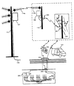
[0053] FIG. 1 illustrates a faulted circuit indicator monitoring system in
accordance with an aspect of the present invention. A number of overhead
faulted circuit indicators 207 each contain a two-way radio that
communicates the occurrence of a fault via a short range antenna 203 to a
local site 110 having an intelligent module 106 installed within radio range
of
the faulted circuit indicators 207. The intelligent module then uses the
existing wired telephone network (not shown) to communicate the fault
occurrence to a remote site 112. Alternatively, the intelligent module may
include a radio interface unit associated therewith for communication with an
antenna 114b to communicate the fault occurrence to a remote site 112
having another long range RF antenna 114a. The remote site 112 includes
a remote intelligent module 107, which may be connected to another site
(not shown) via a wired connection 116. When a fault is detected by a
faulted circuit indicator, the occurrence is relayed in the manner described
above to the remote site 112, triggering the dispatch of a team to the fault
11
CA 02654412 2008-11-19
WO 2007/137205 PCT/US2007/069312
site. The user then uses a wireless device 102 (e.g., a wireless handheld
device). In another embodiment, the wireless device may be located in a
vehicle 104 to determine which conductor 205 is faulted.
[0054] Note that the conductors could also be located in an underground
vault 200, which may be accessible through a manhole 118. Faulted circuit
indicators 206 attached to the underground conductors 210 are wired to a
radio interface unit 400 with a short range antenna 202 to communicate with
the wireless device 102 or wireless device installed in a vehicle 104. In one
embodiment, the short range antenna 202 may be part of or separate from
the radio interface unit.
[0055] Referring to the drawings and to FIGS. 2A and 2B in particular, a
wireless device 102 communicates 904 with eight installations of faulted
circuit indicators 200a-200h. As illustrated, each installation of faulted
circuit
indicators consists of a radio interface unit, and four separate groups
("ways") of faulted circuit indicators, wherein each group has three faulted
circuit indicators, one for each phase. For example, the installation shown at
200e, as shown in FIGS 2A and 2B includes four separate groups 206a-d of
faulted circuit indicators connected to a radio interface unit 400e through
cables 220e with a separate short range antenna 202e connected through
cable 208e. This radio interface unit 400e may include a particular setting
such that it may be differentiated from the other radio interface units. For
example, this identification setting may be in the form of a designation
setting (e.g., serial number), whereupon each particular radio interface unit
has a particular designation (e.g., a particular serial number). In another
12
CA 02654412 2008-11-19
WO 2007/137205 PCT/US2007/069312
embodiment, the identification setting may be in the form of an address
setting (e.g., a media access control (MAC) address). In yet another
embodiment, in order to ensure proper differentiation among a plurality of
units, each radio interface unit may include both a designation setting and an
address setting. For example, both the radio interface unit 400b and radio
interface unit 400e may be associated with a particular address (e.g.,
address 5). In order to differentiate between these radio interface units 400b
and 400e, each radio interface unit 400b and 400e is given a particular
designation setting (e.g., particular serial numbers). In this way, radio
interface units may be differentiated.
[0056] Each faulted circuit indicator within these separate groups 206a-d
may be used to monitor the various phases (e.g., commonly referred to as
the A, B, C phases) associated therewith. For example, each of the faulted
circuit indicators associated with way 206a may be used to monitor the three
phases associated therewith. Through this system, the installation 200e of
faulted circuit indicators 206a, 206b, 206c, 206d may communicate with
wireless device 102.
[0057] Additionally, the wireless device 102 may alternatively be adapted to
communicate with radio interface units associated with overhead fault circuit
indicators as illustrated in FIG. 1. In yet another embodiment, the wireless
device may be in the form of a personal digital assistant (PDA) with a
wireless interface, a laptop computer or a handheld computer with a wireless
interface, etc. and may optionally be mounted in a service vehicle.
[0058] Referring back to FIG. 1, various components of the faulted circuit
13
CA 02654412 2008-11-19
WO 2007/137205 PCT/US2007/069312
indicator monitoring system may be located in an underground vault 200 and
only accessible through a manhole 118. As discussed above, the
underground vault 200 is often susceptible to external elements and even
flooding. Accordingly, its contents are also susceptible to external elements
such as water. Likewise, overhead FCI systems also include electronic
devices which are exposed to external elements. Accordingly, it is also
desirable that any connections between the electronic devices be wireless
and/or waterproof. Moreover, it is also desirable that the communication
members (e.g., probes or other wireless connection means) and
corresponding detection devices be substantially self-contained.
[0059] For example, it is desirable that any connection between each FCI
206 and the radio interface unit 400 of the previous figures be wireless and
waterproof. Also, it is desirable that both the communication members (not
shown) from the FCi 206 and the radio interface unit 400 each be
substantially self-contained.
[0060] Referring to FIG. 4, the radio interface unit 400a includes a housing
402a which is substantially self-contained. Contained within the housing
402a are electronic components (not shown). The electronic components
contained within the housing 402a may further be encapsulated using an
encapsulate material such as potting material. Encapsulate material
provides a physical barrier around the electronic components. This barrier is
malleable, providing increased resistance to shock and vibration. In
addition, if the material is properly cured, the barrier will be water-tight.
14
CA 02654412 2008-11-19
WO 2007/137205 PCT/US2007/069312
[0061] One such encapsulate material is referred to as potting material.
Potting material may include epoxy based materials, urethane based
materials, silicone based materials, acrylic based materials, polyester based
materials, and others. Urethane and silicone based materials are the types
used most often in the electronics industry. Each particular type of potting
material has its own strengths and weaknesses.
[0062] With the exception of the opening for antenna 208a, there are
generally no outlets or openings in the housing 402a. Accordingly, the
housing 402a is substantially self-contained (sealed from the elements). For
example, address switch 414a and power switch 406a are separate and
apart from the housing 402a in that they do not require any mechanical or
electrical connection to any electronic component contained within the
housing 402a. The housing 402a further defines cavities (e.g., at 304a) for
receiving communication members which may be in the form of inductor coil
probes (e.g., at 508a) in a manner in which they do not expose the electronic
components contained within the housing 402a to the external environment.
Housing 402a may further include a securing member such as a connector
socket 408a in order to secure the inductor coil probe 508a within the cavity
304a. Although inductor coil probes are illustrated and described herein, it
is
intended that any communication member which includes an inductor and
produces a magnetic field or communicates information via a magnetic field
may be used in place thereof.
[0063] The inductor coil probes (e.g., at 508a) which interface the cavities
(e.g., at 304a) are coupled to a detection device such as an FCI as
CA 02654412 2008-11-19
WO 2007/137205 PCT/US2007/069312
described with regards to FIG, 1. The inductor coil probes (e.g., at 508a) are
also substantially self-contained. The inductor coil probes (e.g., at 508a)
wirelessly communicate with the radio interface unit 400a via cavities (e.g.,
304a) in the manner described below.
(0064] One particular advantage to having inductor coil probes (e.g., at 508a)
which interface the cavities (e.g., at 304a) without a wired or electrical
connection, is that the system is closer to being intrinsically safe. Because
so-called waterproof connections that require electrical and mechanical
connection between the two devices fail after time, the electrical connection
may become exposed, and pose a safety risk.
[0065] FIGS. 5A and 5B illustrate one embodiment of the hardware
arrangement for the circuitry described with respect to FIG. 3 having an
interface between an inductor coil probe 508b and a radio interface device
400b. Contained within the housing 402b are various electronic components
of the radio interface unit 400b. The electronic components are further
encapsulated by an encapsulate material 514b such as a potting material.
The housing 402b further defines a plurality of cavities (e.g., at 304b) for
receiving inductor coil probes (e.g., at 508b) in a manner in which they do
not expose the electronic components contained within the housing 402b to
the external environment. Further provided are a printed circuit board 520b
which includes a plurality of magnetic field sensors such as hall-effect
sensors (e.g., at 320b) and a printed circuit board 502b which includes a
plurality of inductors (e.g., at 420b) implemented thereon. In this
embodiment, the printed circuit boards 520b and 502b are separate and
16
CA 02654412 2008-11-19
WO 2007/137205 PCT/US2007/069312
distinct. FIGS. 5C and 5D are similar to FIGS. 5A and 5B with the exception
that only one circuit board 520c is implemented and the inductors are in the
form of coiled inductors 420c in the embodiments of FIGS. 5C and 5D.
[0066] During operation of each of the embodiments illustrated in FIGS. 5A-
50, the interface between the inductor coil probes (e.g., at 508 b, c) and the
radio interface unit 400 b, c is as follows. The inductor coil probes (e.g.,
at
508 b, c) may be inserted into the cavities (e.g., at 304 b, c). For example,
as shown in FIGS. 5B and 5D, a magnet 902 b, c is situated at the end of the
inductor coil probe 508 b, c. A corresponding magnetic field sensor (e.g., a
hall-effect sensor) 302 b, c situated on printed circuit board 502b, 520c
detects the presence of a magnetic field from magnet 902 b, c upon insertion
of the inductor coil probe 508 b, c into the cavity 304 b, c. The magnetic
field
sensor 302 b, c produces a signal to the microprocessor, thereby signaling
the presence of an inductor coil probe 508 b, c. A spacer 620 b, c is further
provided in order to prevent the magnet 902 b, c from affecting the inductor
coil 604 b, c contained within the inductor coil probe 508 b, c. Although a
hall-effect sensor is described herein, other suitable magnetic field sensors
may also be implemented such as a Reed switch and the like.
[0067] The inductor coil probes 508b, c which interface with the cavities
304b, c are coupled to a detection device such as an FCI as described in
FIG. 1. The inductor coil probe 508 b, c includes an inductor coil 604 b, c
and is also substantially self-contained. The inductor coil probes 508 b, c
wirelessly communicate with the radio interface unit 400 b, c via cavities 304
17
CA 02654412 2008-11-19
WO 2007/137205 PCT/US2007/069312
b, c by magnetic field or electromagnetic field induction (also referred to as
"magnetic field induction") in the manner described below.
[0068] As illustrated in FIG. 6, during operation, a trip current signal IT is
sent
from a detection device, such as an FCI 206, when a conductor (e.g., 210 of
FIG. 1) related thereto exceeds a select current threshold (e.g., upon an
occurrence of a ground fault). The trip current signal IT induces a magnetic
field 540 at the inductor coil L1 of the inductor coil probe 508d. The
magnetic field 540 from the trip current IT induces a current 11 in inductor
coil
420d of the radio interface unit. This induced current further induces a
voltage V, across load 538d. Information regarding the increased voltage V,
across load 538d may be transmitted from the radio interface unit to a
wireless handheld unit to signal a trip signal by an FCI.
[0069] Alternatively, a reset current signal IR may be sent from a detection
device such as an FCI 206 after the current in a conductor (e.g., 210 of FIG.
1) is restored from a previously tripped condition. In order to distinguish
between the reset current signal IR and the trip current signal IT, these
signals may be sent or established in opposite directions. The reset current
signal lR induces a magnetic field 540 at the inductor coil L1 of the inductor
coil probe 508d. The magnetic field 540 from the reset current IR induces a
current I, in inductor coil 420d of the radio interface unit, This induced
current further induces a voltage V, across load 538d. Information regarding
the decreased voltage V, (as opposed to an increased voltage V, for a trip
signal) across load 538d may be transmitted from the radio interface unit to
the wireless handheld unit to signal a reset signal by an FCI.
18
CA 02654412 2008-11-19
WO 2007/137205 PCT/US2007/069312
(0070] Nevertheless, communication members having a single probe as
discussed in the previous figures are often susceptible to magnetic or
electromagnetic field interference from external sources. For example, as
illustrated in FIG. 7, an interfering magnetic field 532 may be produced by an
adjacent power line 534 carrying high current 530. The interfering magnetic
field 532 may induce a current in inductor coil 420e of the radio interface
unit. This induced current further induces a voltage V1 across load 538e,
and thereby produces a false trip or reset signal.
[0071] As illustrated in FIG. 8, the interfering magnetic field 532 may be
cancelled using a differential inductor coil configuration. In this
arrangement,
the communication member includes two inductor coils 420f and 420g which
are connected in opposite directions. The interfering magnetic field 532
induces a current l1 in inductor coil 420f and a current 12 in inductor coil
420g
of the radio interface unit. The currents i, and 12 are induced in opposite
directions and each induce a voltage V1 in opposite polarity to each other
across load 538f. Accordingly, this arrangement provides for a net induced
voltage of 0, thereby compensating for interference from a magnetic field
and thereby negating false signals.
[0072] Referring to FIG. 9, a radio interface unit 400h is provided for
accommodating a differential inductor coil probe for cancelling interfering
magnetic fields. The substantially self-contained construction of the housing
400h may be generally similar to the housing 402h described with respect to
FIG. 4. Accordingly, the housing 402h further defines cavities (e.g., at
304h) for receiving differential inductor coil probes (e.g., at 609) having
dual
19
CA 02654412 2008-11-19
WO 2007/137205 PCT/US2007/069312
prongs in a manner in which they do not expose the electronic components
contained within the housing 402h to the external environment.
[0073] In another embodiment, the radio interface unit 400a may be provided
for accommodating a differential inductor coil for cancelling interfering
magnetic fields. This embodiment is similar to that described above in
conjunction with FIG. 9, except that each socket 408a includes only a single
cavity 304a to accept the single inductor coil probe 508a. Instead of having
a differential inductor coil probe for each probe 508a, there is a single
differential inductor coil for cancelling interfering magnetic fields.
(0074] The differential inductor coil probes (e.g., at 609) which interface
the
cavities (e.g., at 304h) are coupled to a detection device such as an FCI as
described with regards to FIG. 1. The differential inductor coil probe 609 is
also substantially self-contained. The differential inductor coil probes
(e.g.,
at 609) wirelessly communicate with the radio interface unit 400h via cavities
(e.g., 304h) in the manner described below.
[0075] FIGS. 1OA and 1OB illustrate one embodiment of the hardware
arrangement for the circuitry described with respect to FIG. 8 having an
interface between the differential inductor coil probe and the cavity.
Contained within the housing 402i are various electronic components of the
radio interface unit 4001. The electronic components are further
encapsulated by an encapsulate material 514i such as a potting material.
The housing 402i further defines a plurality of cavities (e.g., at 304i) for
receiving differential inductor coil probes (e.g., at 609i) in a manner in
which
they do not expose the electronic components contained within the housing
CA 02654412 2008-11-19
WO 2007/137205 PCT/US2007/069312
4021 to the external environment. Further provided is a printed circuit board
5021 which includes a plurality of magnetic field sensors such as hall-effect
sensors (e.g., at 3021) and a plurality of inductors (e.g., at 4201)
implemented
thereon. FIGS. 10C and 10D are similar to FIGS. 1OA and 10B with the
exception that the inductors 506k of FIG. IOC and 10D are in the form of
coiled inductors.
[0076] During operation of each to the embodiments illustrated in FIGS. 1 OA-
D, the interface between the differential inductor coil probes 609 i, k and
the
radio interface unit 400 i, k is as follows. The differential inductor coil
probes
609 i, k may be inserted into the cavities 3041, k. For example, as shown in
FIGS. 9B and 9D, a magnet 902 i, k is situated between the prongs of
differential inductor coil probe 609 i, k. A corresponding magnetic field
sensor (e.g., hall-effect sensor 302 i, k) situated on printed circuit board
502
i, k detects the presence of a magnetic field from magnet 9021, k upon
insertion of the differential inductor coil probe 609 i, k into the cavity 304
i, k.
The hall-effect sensor 302 i, k produces a signal to the microprocessor,
thereby signaling the presence of a differential inductor coil probe 609 i, k.
Although a hall-effect sensor is described herein, other suitable elements
may be implemented (e.g., a Reed switch).
[0077] The differential inductor coil probes 609 1, k which interface the
cavities 304 i, k are coupled to a detection device such as an FCI as
described with regards to FIG. 1. The differential inductor coil probe 609 i,
k
includes an inductor coil 604 i, k in each prong and is also substantially
self-
contained. The differential inductor coil probes 609 1, k wirelessly
21
CA 02654412 2008-11-19
WO 2007/137205 PCT/US2007/069312
communicate with the radio interface unit 400 i, k via cavities (e.g., 304 i,
k)
by magnetic field induction in the manner described below.
[0078] FIG. 11 illustrates one embodiment which implements the differential
coil configuration of FIG. 8. In this arrangement, the differential inductor
coil
probe 609a is in a parallel inductor coil configuration. During operation, two
inductor coils 420a and 420b are connected in parallel in opposite directions.
The interfering magnetic field (not shown) induces a current I, in inductor
coil
420a and a current 12 in inductor coil 420b of the radio interface unit. The
currents I, and 12 are induced in opposite directions and each induce a
voltage V, in opposite polarity to each other across load 538, thereby
canceling the respective voltages. Accordingly, this arrangement provides
for a net induced voltage of 0, thereby compensating for interference from a
magnetic field and negating false signals.
[0079] The arrangement of FIG. 11, in effect, forms a differential pulse
transformer configuration 558a, whereupon high-energy, short-lasting pulses
are transmitted with low distortions. During operation, a trip current signal
IT
is sent from a detection device such as an FCI 206 when a conductor (e.g.,
210 of FIG. 1) related thereto exceeds a select current threshold (e.g., upon
an occurrence of a ground fault) via cable 220 into differential inductor coil
probe 609a with series load resistors R. The inductor coils L1 and L2 are
connected in parallel to generate magnetic fields 540a and 540b in opposite
directions. The trip current signal IT induces magnetic fields 540a and 540b
in opposite directions. The magnetic fields 540a and 540b from the trip
current IT induces currents 11 and 12 in inductor coils 420a and 420b of the
22
CA 02654412 2008-11-19
WO 2007/137205 PCT/US2007/069312
radio interface unit, The induced currents 11 and 12 further induce a
differential voltage AV across load 538. Information regarding a positive
differential voltage AV across load 538 may be transmitted from the radio
interface unit to the wireless handheld unit to signal a trip signal by an
FCI.
[0080] Alternatively, a reset current signal IR may be sent from a detection
device such as an FCI 206 after the current in a conductor (e.g., 210 of FIG.
1) is restored from a previously tripped condition. In order to distinguish
between the reset current signal IR and the trip current signal 1T, these
signals may be sent or established in opposite directions. The reset current
signal IR induces magnetic fields 540a and 540b in opposite directions. The
magnetic fields 540a and 540b from the reset current IR induces currents 11
and 12 in inductor coils 420a and 420b of the radio interface unit. The
induced currents I1 and 12 further induce a differential voltage AV across
load
538. Information regarding a negative differential voltage AV across load
538 may be transmitted from the radio interface unit to the wireless handheld
unit to signal a reset signal by an FCI.
[0081] In yet another embodiment, FIG. 12 illustrates another embodiment
which implements the differential coil configuration of FIG, S. In this
arrangement, the differential inductor coil probe 609c is in a serial inductor
coil configuration. During operation, two inductor coils 420a and 420b are
connected in series in opposite directions. The interfering magnetic field
(not
shown) induces a current 11 in inductor coil 420a and a current 12 in inductor
coil 420b of the radio interface unit. The currents 11 and 12 are induced in
opposite directions and each induce a voltage V1 in opposite polarity to each
23
CA 02654412 2008-11-19
WO 2007/137205 PCT/US2007/069312
other across load 538, thereby canceling the respective voltages.
Accordingly, this arrangement provides for a net induced voltage of 0,
thereby compensating for interference from a magnetic field and negating
false signals.
[00821 The arrangement of FIG. 12, in effect, forms a differential pulse
transformer configuration 558a, whereupon high-energy, short-lasting pulses
are transmitted with low distortions, Because the inductor coils L1 and L2
are connected in series, the design values thereof are generally lower than
the parallel arrangement of FIG. 11 due to the additive or period inductance.
During operation, a trip current signal IT is sent from a detection device
such
as an FCI 206 when a conductor (e.g., 210 of FIG. 1) related thereto
exceeds a select current threshold (e.g., upon an occurrence of a ground
fault) via cable 220 into differential inductor coil probe 609a with series
damping ringing pulse resistors R. The inductor coils L1 and L2 are
connected in series to generate magnetic fields 540a and 540b in opposite
directions. The trip current signal IT induces magnetic fields 540a and 540b
in opposite directions. The magnetic fields 540a and 540b from the trip
current IT induces currents 11 and 12 in inductor coils 420a and 420b of the
radio interface unit. The induced currents 11 and 12 further induce a
differential voltage AV across load 538. Information regarding a positive
differential voltage AV across load 538 may be transmitted from the radio
interface unit to the wireless handheld unit to signal a trip signal by an
FCI.
[0083] Alternatively, a reset current signal IR may be sent from a detection
device such as an FCI 206 after the current in a conductor (e.g., 210 of FIG.
24
CA 02654412 2008-11-19
WO 2007/137205 PCT/US2007/069312
1) is restored from a previously tripped condition. In order to distinguish
between the reset current signal IRand the trip current signal IT, these
signals may be sent or established in opposite directions. The reset current
signal IR induces magnetic fields 540a and 540b in opposite directions. The
magnetic fields 540a and 540b from the reset current IR induces currents I,
and 12 in inductor coils 420a and 420b of the radio interface unit. The
induced currents 11 and 12 further induce a differential voltage AV across
load
538. Information regarding a negative differential voltage AV across load
538 may be transmitted from the radio interface unit to the wireless handheld
unit to signal a reset signal by an FCI.
[0084] FIG. 13 illustrates another embodiment which implements the
differential coil configuration of FIG. 8. In this arrangement, a trip current
IT
or a reset current IR signal from the differential inductor coil probe 609a
generates equal and opposite magnetic fields 540a and 540b. The magnetic
fields 540a and 540b induce currents Ii and 12 in the radio interface unit. A
detection circuit 559a is further provided with symmetrical network branches
having inputs 580a and 580b coupled to inductor coils 420a and 420b.
Symmetrical ends 582a and 582b are further coupled to a latching flip-flop
G1/G2 and a microcontroller 310. Each symmetric network branch includes
a series diode; an amplitude control element such as a shunt diode or a
shunt resistor; a low pass filter; and a charging circuit (or charge holding
circuit). In an embodiment of the detection circuit 559a, shunt diodes D1 and
D3 are the amplitude control elements for the incoming pulse, whereas the
CA 02654412 2008-11-19
WO 2007/137205 PCT/US2007/069312
low pass filter and charging circuit is formed by a network of resistors and
capacitor.
[0085) More specifically, the direction of the voltage/current peak from an
induced pulse is detected with four diodes (D1, D2, D3 and D4) at inputs
580a and 580b, respectively. A positive pulse U3 FIG. 13AH (at D3 and D4)
is directed through resistor R4 into capacitor C2, storing the charge.
Resistor R5 or R2 allows capacitor discharging of positive pulse U3 in a
controlled manner, preventing false latching from ringing currents from the
FCI and probe circuits (e.g., L1, L2 and R). A negative pulse U1 FIG,13Ai
is conducted through diode D1, with diode D2 blocking any residual voltage
from getting into capacitor C1 through clamping in diode D1 and reverse bias
rectification in diode D2. Diode D1 clamps the negative pulse at about -0.5
V to -0.8 V, depending on the diode type.
[0086] The R4/C2 (and R1/C1) components create a low-pass filter,
preventing high frequency spikes changing the logic state of the flip-flop
gates G1/G2 (NOR gate flip flops). The positive pulse U3 generates a
current, through R4, which charges capacitor C2. Resistors R6 and R3 each
prevent latch-up of respective CMOS gates G2 and G1, and allow charging
capacitors C1 and C3 to reach a higher voltage above the internal CMOS
gates clamping voltage. Charging and retaining charge is important in
preventing undesired flip-flop action due to ringing in the Trip/Reset pulses.
In this arrangement, NOR gates G1 and G2 are further connected in an R-S
flip-flop configuration, with active-high inputs.
26
CA 02654412 2008-11-19
WO 2007/137205 PCT/US2007/069312
[0087] Pulse U4 FIG, 13Bii is applied to gate G2 input 587 of the flop-flop.
If
the flip-flop outputs logic 0 on GI at output 587, prior to the trip pulse,
the
pulse changes the logic state of line 550 from logic 0 to logic 1, The status
of
the flip-flop is evaluated with a microprocessor 310 at I/O interface 552. The
microprocessor 310 such as a Texas Instruments MSP430 family is suitable
for this application where a standard program can be written.
[0088] On a power-up, flip-flop G1/G2 sets a random output logic level on
line 550. Resistor R7, serial with the GI output, allows for resetting of the
flip-flop G1/G2 with the microprocessor 310. A program may further be
provided for driving the microprocessor 310, changing the I/O interface 552
from input to output, and setting line input 550 with a logic 0. If, at the
same
time, the gate G1 outputs logic 1, the resistor R7 allows voltage at gate G2
input 587 to drop below the threshold level of logic 0, causing flip-flop
G1/G2
to change the G1 output to logic 0. This circuit arrangement allows reusing
the same line 550 to read logic data from flip-flop G1/G2 and resetting the
flip-flop G1/G2, with a single copper trace line input 550 and a single reset
resistor R7.
[0089] The flip-flop NOR gates G1/G2 may further create a CMOS memory
location, thereby allowing for latching and storage of logic values for month
and years. CMOS inherently uses a relatively small supply current, thereby
allowing for extension of the lifetime of a supply battery.
100903 A ringing pulse from a trip pulse or a reset pulse can often cause
false
latching. The arrangement of FIG. 13 provides for an embodiment which
suppresses such false latching. FIGS, 14A-14C depict the progression of a
27
CA 02654412 2008-11-19
WO 2007/137205 PCT/US2007/069312
ringing pulse exiting the detection circuit of FIG. 13 and the suppression of
false latching caused by ringing.
[0091] The arrangement of FIG. 13 is designed to accept a trip/reset pulse
from a various FCI sensors and differential inductor coil probes. Such
hardware diversification may result in a trip or reset pulse with multiple
ringing portions such as 560b, 564a and 566b in induced pulse U1, and
560c, 564c and 566c in induced pulse U3 shown in FIGS. 13Ai and 13Aii. In
effect, induced pulses U1 and U3 generated by differential pulse transformer
558a at both ends of the coil pair (e.g., inductor coils 420a and 420b) will
be
of similar amplitude and reversed polarity in the absence of shunt diodes D1
and D3 and series diodes D2 and D4 (shown as dotted lines).
[0092] Shunt diodes D1 and D3 may be used to clamp a negative pulse,
whereas series diodes D2 and D4 may be used to rectify and pass a positive
pulse in forward bias. Diode pairs D1 and D2 clamp and rectify negative and
positive pulse portions 560a, 564a and 566a in a reversed polarity induced
pulse U1. Diode pairs D3 and D4 rectify and clamp positive and negative
pulse portions 560c, 564b and 566c, respectively, in a positive polarity
induced pulse U3.
[0093] FIG. 14Bi depicts the voltage of pulse U2 across capacitor CI,
induced by a ringing pulse U1. An erred latching of the flip-flop G11G2 may
result if the voltage of pulse U2 reaches above the logic I threshold 570.
The desired positive polarity induced pulse U3 depicted in FIG. 14Aii with a
higher amplitude generates filtered pulse U4 across capacitor 02 as shown
in FIG. 14Bii, that in turn generates logic I for gate G2. The charge of pulse
28
CA 02654412 2008-11-19
WO 2007/137205 PCT/US2007/069312
U4 across capacitor C2 holds longer than the later charging of ringing pulse
U2 across C1 as shown in FIG. 14Bi.
[0094] FIG, 14c superimposes pulses U2 and U4 presented to the flip-flop
G1/G2 to illustrate the concept that an extended logic 1 level of pulse U4
presented to gate G2 outlasts a false logic I caused by ringing pulse U2
presented to gate G1, thus preserving a proper logic latch by the flip-flop
G1/G2. The time constant of the C2/R5/R6 (or C11R21R3) allows for rejection
of most false ringing voltage of pulse U2 by a voltage margin 572, and a time
margin 574 depending on the amplitude differences of pulses U4 and U2 set
at the logic level in G1IG2. The diode pair and RC network in differential
arrangement allows for error-free detection of the desired induced pulse U4
under the presence of a "ringing" signal U2 on the opposite side of the
differential pulse transformer 558. The same principle of operation applies if
the induced pulses U1 and U3 are of reverse polarity, except that the pulses
in FIGS 14a to 14c will be interposed between U1 and U3, and between U2
and U4. The teachings described in relation to FIGS. 13 and 14 may further
be implemented for a single probe differential coil configuration without
deviating from the spirit of the present invention.
[0095] Further according to the present invention, it is envisioned that any
type of detection device that is capable of sending a positive and a negative
signal may be used in conjunction with or in place of the radio interface
unit.
Some examples of detection devices (other than an FCI) that may be used
include: water, high voltage electric field, specific gravity, light, and
sound,
gas sensors such as CO, C02, SOx, NOx, Ammonia, Arsine, Bromine,
29
CA 02654412 2008-11-19
WO 2007/137205 PCT/US2007/069312
Chlorine, Chlorine Dioxide, VOCs, Combustibles, Diborane, Ethylene Oxide,
Fluorine, Formaldehyde, Germane, Hydrogen, Hydrogen Chloride, Hydrogen
Cyanide, Hydrogen Fluoride, Hydrogen Selenide, Hydrogen Sulfide, Oxygen,
Ozone, Methane, Phosgene, Phosphine, Silane, and the like; pressure
sensors for sensing, for example, pressure in a gas line, water line, waste
line, oil line, and the like; temperature sensors; electromagnetic radiation
sensors; radiation sensors; smoke sensors; particulate matter sensors; liquid
phase sensors such as pH, turbidity, Br-, Ca2+, Cl-, CN-, Cu2+, F-, I-, K+,
Na+, NH4+, N03-, Pb2+, S-(AG+), conductivity sensors, and the like; radio
wave sensors; electrical sensors such as under voltage sensors, over
voltage sensors, under current sensors, over current sensors, frequency
sensors and the like; power factor alarms; demand overload indicators;
sensors that detect the presence of primary system voltage; sensors that
determine if a sealed subsurface fuse has operated by sensing voltage on
each side of fuse element with loss of load current; sensors that sense the
open or closed position of a subsurface switch; voltage sensors which
monitors status of lead-acid batteries used to run controller or motor
operators for subsurface switches; power quality sensors which detect
primary voltage swells and sags along the distribution system, and other
sensors that detect power quality issues and send an alarm status.
(00961 The detection device communicates with the radio interface unit 400
according to any of the embodiments herein described. Thus, the monitoring
system of the present invention may be used to monitor states or conditions
CA 02654412 2008-11-19
WO 2007/137205 PCT/US2007/069312
that are detected with any of the detection devices (e.g., FCIs or other
sensors) mentioned above.
[0097] It is a further aspect of this invention that the faulted circuit
indicator
monitoring system differentiate between the different types of detection
devices that may be in communication with the radio interface unit 400. The
differentiation may be performed between two different types of detection
devices using the permanent magnet (e.g., at 902b, 902c, 902i, or 902k) of
the inductor coil probes (e.g., at 508a, 508b, 508c, 609, 609i, or 609k) and
the magnetic field sensor (e.g., 302b, 302c, 302i, or 302k). The polarity of
the permanent magnet (e.g., at 902b, 902c, 902i, or 902k) for a particular
type of detection device may be a polar opposite from the permanent
magnet (e.g., at 902b, 902c, 902i, or 902k) for another particular type of
detection device. The radio interface unit 400 may then be configured to
transmit the status of only one particular type of detection device when
interrogated by a specific wireless device 102 (or when the wireless device
702 interrogates using a specific algorithm), and transmit the status of
another particular type of detection device when interrogated by another
specific wireless device 102 (or when the wireless device 102 interrogates
using another algorithm).
[0098] For example, the radio interface unit 400 may be mounted in a vault
200 containing electrical conductors for an electrical power utility, and
access to water lines for a water utility. Faulted circuit indicators may be
used to monitor faulted circuits on the electrical conductors, and may be in
communication with the radio interface unit 400 using the various probe
31
CA 02654412 2008-11-19
WO 2007/137205 PCT/US2007/069312
systems described herein. However, the inductor coil probes (e.g., at 508a,
508b, 508c, 609, 609i, or 609k) for the faulted circuit indicators would be
configured such that the permanent magnets (e.g., at 902b, 902c, 902i, or
902k) have a common pole (north) facing the magnetic field sensor (e.g.,
302b, 302c, 302i, or 302k). If the radio interface unit 400 has twelve
connector sockets (e.g., 408a, 408h), less then all of them may be used
used by the faulted circuit indicators. The magnetic field sensors (e.g.,
302b,
302c, 3021, or 302k) would sense that all of these inductor coil probes (e.g.,
at 508a, 508b, 508c, 609, 609i, or 609k) have permanent magnets (e.g., at
902b, 902c, 9021, or 902k) with a common polarity.
[0099] The radio interface unit 400 may also be in communication with
inductor coil probes (e.g., at 508a, 508b, 508c, 609, 6091, or 609k) from
detection devices for the water utility. For example, the water utility may
want to monitor whether the pressure in the water lines exceeds a threshold.
The water utility could install such detection devices on the water lines, and
have these water pressure detection devices communicate with inductor coil
probes (e.g., at 508a, 508b, 508c, 609, 6091, or 609k) in communication with
the remaining connector sockets (e.g., 408a, 408h) of the radio interface unit
400. The inductor coil probes (e.g., at 508a, 508b, 508c, 609, 6091, or 609k)
from the water utility would include permanent magnets (e.g., at 902b, 902c,
9021, or 902k) having a common pole (south) facing the magnetic field
sensor (e.g., 302b, 302c, 302i, or 302k). The pole of the permanent
magnets (e.g., at 902b, 902c, 902i, or 902k) facing the inductor coil probes
(e,g., at 508a, 508b, 508c, 609, 609i, or 609k) of the water utility would be
32
CA 02654412 2008-11-19
WO 2007/137205 PCT/US2007/069312
opposite the pole of the permanent magnets (e.g., at 902b, 902c, 902i, or
902k) facing the inductor coil probes (e.g., at 508a, 508b, 508c, 609, 609i,
or 609k) of the electric utility. In this way, the radio interface unit 400
could
differentiate between detection devices of different utilities, and transmit
information relating only to the utility that interrogates the radio interface
unit
400.
[00100] The radio interface unit 400e may include a particular identification
setting such that it may be differentiated from the other radio interface
units.
For example, this identification setting may be in the form of a designation
setting (e.g., serial number), whereupon each particular radio interface unit
has a particular designation (e,g., a particular serial number). In another
embodiment, the identification setting may be in the form of an address
setting (e.g., a media access control (MAC) address). In yet another
embodiment, in order to ensure proper differentiation among a plurality of
units, each radio interface unit may include both a designation setting and an
address setting. For example, both radio interface unit 400b and radio
interface unit 400e may be associated with particular address (e.g., address
5). In order to differentiate between these radio interface units 400b and
400e, each radio interface unit 400b and 400e is given a particular
designation setting (e.g., particular serial numbers). In this way, radio
interface units may be differentiated.
00101] Referring back to the drawings and to FIGS. 2A and 2B in particular, a
wireless device 102 communicates 904 with eight installations of faulted
circuit indicators 200a-200h. As illustrated, each installation of faulted
circuit
33
CA 02654412 2008-11-19
WO 2007/137205 PCT/US2007/069312
indicators consists of a radio interface unit, and four separate groups
("ways") of faulted circuit indicators, wherein each group has three faulted
circuit indicators, one for each phase. For example, the installation shown at
200e, as shown in FIGS 2A and 2B includes four separate groups 206a-d of
faulted circuit indicators connected to a radio interface unit 400e through
cables 220e with a separate short range antenna 202e connected through
cable 208e. This radio interface unit 400e may include a particular setting
such that it may be differentiated from the other radio interface units. For
example, this identification setting may be in the form of a designation
setting (e.g., serial number), whereupon each particular radio interface unit
has a particular designation (e.g., a particular serial number). In another
embodiment, the identification setting may be in the form of an address
setting (e.g., a media access control (MAC) address), In yet another
embodiment, in order to ensure proper differentiation among a plurality of
units, each radio interface unit may include both a designation setting and an
address setting. For example, both the radio interface unit 400b and radio
interface unit 400e may be associated with a particular address (e.g.,
address 5). In order to differentiate between these radio interface units 400b
and 400e, each radio interface unit 400b and 400e is given a particular
designation setting (e.g., particular serial numbers). In this way, radio
interface units may be differentiated.
x0102] Each faulted circuit indicator within these separate groups 206a-d
may be used to monitor the various phases (e.g., commonly referred to as
the A, B, C phases) associated therewith. For example, each of the faulted
34
CA 02654412 2008-11-19
WO 2007/137205 PCT/US2007/069312
circuit indicators associated with way 206a may be used to monitor the three
phases associated therewith. Through this system, the installation 200e of
faulted circuit indicators 206a, 206b, 206c, 206d may communicate with
wireless device 102.
[00103] In one embodiment in which the identification setting of each radio
interface unit is an address setting, the address setting of a radio interface
unit 400 may be adjusted by simply turning the address dial 414 as
illustrated in FIG. 4a and 4b. Although this embodiment specifically
describes the setting in the form of an identification setting and, more
particularly an address setting, the setting to be adjusted may be any
setting,
(e.g., a designation setting, power setting, communication setting, etc.).
Moreover, although a dial is specifically shown, any actuator is suitable
(e.g,,
a linear multi-position switch instead of a dial).
[00104] The address dial 414 may also be self-contained. Accordingly, the
address dial does not mechanically or electrically engage any of the internal
electronic components contained within the housing 402 of the radio
interface unit. This allows for the housing 402 of the radio interface unit to
be substantially self-contained. As such, the substantially self-contained
housing 402 allows the radio interface unit 400 to be submergible and
capable of withstanding harsh environments. This arrangement is an
example of a system for adjusting the settings of a power system device
using a magnetically coupled actuator.
00105] More specifically, FIG 15 illustrates the address dial of FIG 4a and
4b.
The address dial generally includes a plurality of magnets situated in a
select
CA 02654412 2008-11-19
WO 2007/137205 PCT/US2007/069312
arrangement. By turning the address dial 414, the plurality of magnets may
be situated in various select arrangements. The select arrangements may
correspond to various select addresses. In the illustrated embodiment,
turning the address dial 414 in the counter-clockwise direction progresses
through the various addresses in increasing order. Alternatively, the radio
interface unit may be configured such that turning the address dial 414 in the
clockwise direction progresses through the various addresses in increasing
order.
[00106] In an embodiment, the magnetically coupled address dial 414 has a
start position at 901 and a circular rotatable dial with a plurality of
embedded
magnets (e.g, 902a to 902d). The arrangement of magnets may correspond
to select addresses. More specifically, when the magnets are coupled to
one or more magnetic field sensors such as Hall effect sensors or Reed
switches 504a, 504b and 504c at positions A, B and C, the select
arrangement of the magnets is detected and a select address corresponding
thereto is provided.
;00107] In an embodiment of the present invention, address dial 414 includes
four magnets 902a to 902d, which may be coupled to three magnetic field
sensors for detecting the select arrangement of the magnets. The Hall effect
sensors or Reed switches 504a to 504c are connected to a microprocessor
310 (FIGs, 6A, 6B, 6C, and 6D) within radio interface unit 400. The
microprocessor processes the select magnet arrangement and provides a
select address corresponding thereto.
36
CA 02654412 2008-11-19
WO 2007/137205 PCT/US2007/069312
[00108] The illustrated embodiment has eight settable positions indicated at
position A as a position pointer 904. The three bits read by Hall effect
sensors or Reed switches 504a, 504b and 504c represent binary addresses
corresponding to select radio interface units. For example, magnets such as
902a and 902b coupled to Hall effect sensors or Reed switches A and B will
form a binary bit of 011. This binary bit provides for a specific binary
address
for the radio interface unit. A binary address table corresponds to the
pointer
position 904 can be constructed as below:
Pointer Position Hall Sensor coupled Binary Address
1 N/C 000
2 AB 091
3 BC 110
4 A 001
AC 101
6 B 010
7 C 100
8 ABC 111
;00709] Fewer or more addresses can be accomplished by using fewer or
more permanent magnets and/or fewer or more Hall effect sensors or Reed
switches in similar arrangement. In an embodiment, the magnetically
coupled address dial 414 magnet and magnetic field sensor position pattern
can be also mirrored or permutated for the same number of addresses.
00110] As shown in FIG. 4A, the radio interface unit 400 may also include a
power dial 406 for effecting the power of the unit. The power dial 406 may
include a magnet, which may be adjustable such that power is supplied to
the radio interface unit when the magnet is coupled to a switch contained in
the housing of the radio interface unit. The power dial 406 may further be
37
CA 02654412 2008-11-19
WO 2007/137205 PCT/US2007/069312
coupled to the address setting dial 414 such that every time the address
setting dial 414 position is changed the power dial 406 will turn to the reset
position to power off the radio interface unit 400. In this manner, the
previous address setting will not be stored.
[00111] In another embodiment, by turning the power dial 406 to "ON"
position, the radio interface unit 400 may be adapted to execute the
following sequence:
[00112] 1) Measure the battery voltage. If the voltage is below a minimum
voltage, then turn off the radio interface unit 400, otherwise save the
measured voltage.
[00113] 2) Perform a complete RAM and Flash diagnostic test and record
the results in RAM
[00114] 3) Read configuration parameters and enter normal operation.
[00115] In an embodiment, the address dial 414 includes a magnetically
coupled address interface that is water tight sealed using potting material.
The magnetically coupled address interface is operable in an environment
exposed to water such as an outdoor, overhead or underground installation.
;00116] FIG 16A depicts a circuit diagram of an embodiment of a magnetically
coupled address interface. As illustrated in FIG. 16A, the address dial 414
includes a magnetically coupled address interface 415a or 415b including an
arrangement of a plurality of magnets 930. When the magnets 930 are
coupled to the magnetic field sensors 910, a select address 918 may be
provided. The various addresses 918 are dependent upon the various
arrangements of the magnets. A microprocessor (or other logic device such
38
CA 02654412 2008-11-19
WO 2007/137205 PCT/US2007/069312
as an FPGA, ASIC, or discrete logic) 310 may further be provided for
processing the select arrangement of magnets and providing addresses 918
corresponding thereto. The microprocessor 310 may further be adapted to
provide a power management output control 916 to activate or deactivate
the biasing circuits 940a or 940b of the magnetic field sensor 910. In an
embodiment, the magnetic field sensors 910 are a plurality of hall-effect
sensors or a plurality of Reed switches.
[00117] In another embodiment, a battery-saving environment for the radio
interface unit is further provided whereupon the magnetic field sensors 910
are turned on momentarily and turned off after the addresses are read. For
example, the radio interface unit may be adapted to turn on upon activation
by a power management control 916 (e.g., the power dial of FIG 5) or upon
receiving an external request command from an external device via the
microprocessor 310.
:00118] In an embodiment, the biasing circuit 940a includes a power source
Vdd, a plurality of pull up resistors (not shown in FIG. 8B) and at least a
transistor such as a P-channel MOSFET 914 that supplies the biasing
voltage VhesNreed to the magnetic field sensor 910. In an embodiment, a
power management control I/O 916 in the microprocessor 310 activates or
deactivates the biasing circuit 940a by controlling the gate voltage of the P-
channel MOSFET 914. Upon an initial power on or a power-on-reset, the
control 1/0 916 activates the biasing circuit 940a to bias the magnetic field
sensor 910 for a brief period such as approximately 100 microseconds to
about 150 microseconds, The biasing voltage VhesNreed is turned off after
39
CA 02654412 2008-11-19
WO 2007/137205 PCT/US2007/069312
the addresses 918 are read by the microprocessor 310. In an embodiment,
subsequent to reading the addresses 918, the control I/O 916 deactivates
the biasing circuit 940a indefinitely until the power management issues a
control I/O 916 to reactivate the biasing circuit 940a.
(00119] The activation or deactivation of the magnetic field sensor 910 may be
controlled by a factory set power management program in the
microprocessor 310 or upon receiving an external request command from an
external device. The external devices may include a hand held terminal,
PDA, cellular phone or laptop host computer, alternatively mounted in a
vehicle. When the biasing circuit 940a is deactivated, the magnetic field
sensor 910 consumes essentially no current, thus extending the battery life.
[00120] FIG. 16B depicts another embodiment of a magnetically coupled
address interface 415b. As shown in FIG. 16B, a biasing circuit 940b
includes connecting the ground to an N-channel MOSFET 915 while the
biasing voltage VhesNreed is connected to Vdd. The biasing circuit is
activated or deactivated through controlling the gate of the N-channel
MOSFET 915. In either embodiments, the transistors used in biasing circuits
940a or 940b can be bipolar transistors or any suitable switching transistors
to perform the activation or deactivation switching function.
00121] FIG. 16C depicts an embodiment of a magnetically coupled address
interface 415c between a plurality of hall-effect sensors to a microprocessor.
In an embodiment, three hall-effect sensors 910a to 910c are used as
magnetic field sensors to sense respective magnets 930a to 930c. The Hall
effect sensors 910a to 910c outputs are open drain and respective pull-up
CA 02654412 2008-11-19
WO 2007/137205 PCT/US2007/069312
resistors R1 to R3 with values ranging from about 1 OkOhm to about
100kOhm connected to the biasing voltage Vhes are used to indicate logic
levels I in respective addresses 918a to 918c to 1/01 to 1/03 of
microprocessor 310. In the presence of magnets 930a to 930c, the Hall
sensors 910a to 91 Oc will give a logic level 0 to the respective addresses
918a to 918c.
[00122] In an embodiment illustrated, the biasing circuit 940c uses a
transistor
such as a P-channel MOSFET 914, a PNP bipolar transistor or any suitable
switching transistor (not shown) to activate or deactivate the biasing circuit
940c. In an alternate embodiment, the biasing circuit 940c uses a transistor
such as a N-channel MOSFET 915, a NPN bipolar transistor or any suitable
switching transistor (not shown) connected to the ground COM_GND to
activate or deactivate the biasing circuit 940c, with the biasing voltage Vhes
connected to Vdd in this scheme. An optional discharging resistor R7, with
values of hundreds of kOhms connected to the ground COM_GND can be
used for discharging any remaining voltages, with Hall effect sensors 910a to
910c are powered down to prevent floating address lines 918a to 918c to
1101 to 1/03 in microprocessor 310.
00123] FIG. 16D depicts another embodiment of a magnetically coupled
address interface 415d between a plurality of Reed switches to a
microprocessor. In an embodiment, three Reed switches 910d to 910f are
used as magnetic field sensor to sense respective magnets 930d to 930f.
The Reed switches 91 Od to 91 Of are connected to respective pull-up
resistors R4 to R6. In the absence of magnet, the pull-up resistors indicate
41
CA 02654412 2008-11-19
WO 2007/137205 PCT/US2007/069312
logic 1 to address lines 918d to 918f. In the presence of magnets 930d to
930f, the Reed switches 910d to 910f close where the currents are shunt to
ground, thus indicating logic 0 in addresses 918d to 918f to 1/01 to 1/03 of
microprocessor 310.
[001241 In an embodiment of battery saving circuit design, the biasing voltage
Vreed can be powered with On/Off control from a microprocessor 1/0 916,
with a higher current buffer 932 or with a P-channel MOSFET 914, a PNP
bipolar transistor or any suitable switching transistor (not shown). The
choice
may be factory set by design. The pull-up resistors R4 to R6 can be in a
range from about 10 kOhm to about 100 kOhm, allowing a relatively weak
voltage source to drive three or more resistors and Reed switches. In the
previous embodiment shown in FIG. 16C, the Hall-effect sensors 910a to
910c cannot be driven from a microprocessor 310 nor from a current buffer
932 as shown in FIG. 16D since relatively high currents are needed to be
driven with a P-channel, or N-channel MOSFETs or any suitable switching
transistor with a proper circuit connection. In an alternate embodiment, the
biasing circuit 940d can use a N-channel MOSFET 915, a NPN bipolar
transistor or any suitable switching transistor (not shown) connected to the
Reed switches ground GND while the biasing voltage Vreed is connected to
Vdd. A discharging resistor R8 of values of hundreds of kOhms connected to
the ground GND may be used for discharging any remaining voltages when
all Reed switches 910d to 910f are open, preventing floating address lines
918d to 918f to 1/01 to 1/03 to microprocessor 310.
42
CA 02654412 2008-11-19
WO 2007/137205 PCT/US2007/069312
[00125] FIG. 17A illustrates an example of a user interface of the wireless
device 102 that may be used in the systems illustrated in FIGS. 2A and 213,
The user interface includes a power indicator 1001, such as a green LED,
which is illuminated when the wireless device 102 is turned on via power
button 1024. In addition, the user interface includes two controls, an
information acquisition control which is implemented as a "scan" button
1012, and an identification setting increment control which is implemented as
a "next" button 1010. The "scan" button 1012 causes the wireless device
102 to scan the nearby area for any radio interface units (e.g., those
associated with the installation of faulted circuit indicators of FIGS. 2A and
2B) that may be present. During the scan, each radio interface unit may be
adapted to communicate its identification setting (e.g., address), its status,
and the status of any faulted circuit indicators that are connected to it.
;00126] Once a scan is completed, a summary of the scan is displayed on a
radio address indicator 1006. The radio address indicator 1006 comprises a
plurality of radio interface unit status indicators. Each LED of the radio
address indicator 1006 may correspond to each radio interface unit
associated with each one of the installations of faulted circuit indicators
200a-h of FIGS, 2A and 2B. The radio interface unit status indicators may
be implemented using eight tri-color LEDs. Depending on the result of the
scan operation, the LEDs within the radio address indicator 1006 will be
illuminated in different ways. If a radio interface unit with a particular
address Is not detected, then the radio address indicator 1006 LED with the
corresponding address will not be illuminated. Conversely, for each radio
43
CA 02654412 2008-11-19
WO 2007/137205 PCT/US2007/069312
interface unit detected, a corresponding LED within the radio address
indicator 1006 will display amber, green or red. A particular LED within the
radio address indicator 1006 displays green if none of the faulted circuit
indicators connected to the particular radio interface unit have detected a
fault. Conversely, a particular LED within the radio address indicator 1006
displays red if any of the faulted circuit indicators connected to the
corresponding radio interface unit have detected a fault. As discussed later,
a particular LED may be illuminated as amber if the corresponding radio
interface unit is presently selected as discussed below.
(00127] The "next" button 1010 allows a user of the wireless device 102 to
sequentially step through each of the radio interface units that the wireless
device 102 detected during its last scan operation. The user interface of the
wireless device 102 also includes a group (way) indicator 1022, which
displays the status of any group of faulted circuit indicators connected to
the
radio interface unit presently monitored by the wireless device 102. The
group (way) indicator 1022 includes a plurality of faulted circuit indicator
status indicators, which as shown, are twelve LEDs 1008. The twelve LEDs
are organized in four rows, each corresponding to one of four separate
groups (ways) of faulted circuit indicators, and three columns, each
corresponding to a separate phase 1014. For example, if the user were to
select the display for radio interface 400e of FIGS. 2A and 213, the group
(way) indicators 1022 will correspond to each group of faulted circuit
indicators 206a-d, whereas if the user were to select the display for radio
interface 400h of FIGS. 2A and 2B, the group (way) indicators 1022 will
44
CA 02654412 2008-11-19
WO 2007/137205 PCT/US2007/069312
correspond to each group of faulted circuit indicators 206e-h. As discussed
above, each of the faulted circuit indicators associated with the particular
group (or way) are generally associated with different phases (e.g., A, B, C
phases) and accordingly will correspond to the LEDs 1008.
[00128] During operation, if a particular faulted circuit indicator is not
faulted,
the corresponding LED will display green. Conversely, if a particular faulted
circuit indicator is faulted, the corresponding LED will display red. And if
the
particular faulted circuit indicator is not connected, the corresponding LED
will not be illuminated.
[00129] The user interface of the wireless device 102 also includes a system
health indicator 1018, which displays information about the health of the
presently selected radio interface unit. One implementation of the system
health indicator 1018 is a bi-color LED, which displays green when there are
no issues with the selected radio interface unit, and red when the selected
radio interface unit has an issue that requires maintenance. In another
embodiment, a tri-color LED may be used to indicate the system life of the
radio interface unit. For example, a green color may indicate that greater
than one year of system life remains. An amber color may indicate that less
than one year of system life remains. A red color may indicate that complete
depletion of system life is imminent. In one embodiment, the system life of
the radio interface unit may equate to the battery life associated therewith.
00130] FIG. 17B illustrates an embodiment of the disclosed user interface
102 after a scan operation has been completed, and the "next" button has
been pushed to display the status of the faulted circuit indicators attached
to
CA 02654412 2008-11-19
WO 2007/137205 PCT/US2007/069312
the radio interface unit with address 5 (e.g., 400e of FIG 2). Among others,
the radio interface unit with address 8 has reported as problem free as,
indicated by the LED 1020 being illuminated as green. Also, the radio
interface unit with address 4 indicates that that unit is either not
installed, or
the radio within the radio interface unit has malfunctioned, as indicated by
the unlit LED 1003.
[00131] For illustration purposes, the status of the faulted circuit
indicators
attached to the radio interface unit with address 5 (e.g., 400e of FIG 2), are
being displayed in the group (way) indicator 1022. This is indicated by LED
1007, which is displayed as amber in the illustrated embodiment. All faulted
circuit indicators in group or way 1 (e.g., 206a of FIGS. 2A and 28), group or
way 2 (e.g., 206b of FIGS. 2A and 2B), and group or way 3 (e.g., 206c of
FIG. 2) are installed, and none have detected faults. Therefore, the
particular LEDs corresponding to those faulted circuit indicators are
illuminated green. For instance, the LED 1016 corresponding to way 2 (e.g.,
206b of FIGS. 2A and 2B), phase C is illuminated green. In addition, the
group (way) indicator 1022 indicates that none of the faulted circuit
indicators
corresponding to group or way 4 (e.g., 206d of FIGS. 2A and 2B) are
installed. In the illustrated embodiment, this is indicated with an unlit LED,
such as the LED 1015 corresponding to group or way 4, phase C. Because,
the faulted circuit indicators corresponding to group or way 4 (206d) are
shown to be connected in FIGS. 2A and 213, this may indicate a problem in
the connection of the faulted circuit indicators.
46
CA 02654412 2008-11-19
WO 2007/137205 PCT/US2007/069312
[00132] In FIG. 17C, the status of the faulted circuit indicators attached to
the
radio interface unit with address 5 are being displayed. However, during the
previous scan, a number of the faulted circuit indicators attached to the
radio
interface unit with address 5 reported a fault condition. For instance, LEDs
1009, 1011, and 1013 all indicate that the faulted circuit indicators
corresponding to those LEDs reported a fault. For illustration purposes, the
faulted circuit indicator associated with phase B of group or way 2 (e.g.,
206b of FIG. 2) is faulted whereas the faulted circuit indicators associated
with phases A and C of group or way 2 (e.g., 206d of FIG. 2) are connected
and not faulted.
[00133] According to one embodiment, the user interface 102 will display on
the group (way) 1022 and phase 1008 indicators the status of the faulted
circuit indicators attached to the radio interface unit that first reports a
faulted circuit. If none of the radio interface units report a faulted
circuit, then
the user interface 102 will display on the group (way) 1022 and phase 1008
indicators the status of the faulted circuit indicators attached to the radio
interface unit with the lowest numbered address. For example, FIG. 17D
indicates that at least one faulted circuit indicator attached to radio
interface
unit at address 3 reports a fault, as well as at least one faulted circuit
indicator attached to radio interface unit at address 8. As soon as the radio
interface unit with address 3 reports a fault, the status of the faulted
circuit
indicators connected to the radio interface unit associated with address 3
will
be displayed on the group (way) and phase 1022, 1008 indicators. In order
to view the status of the faulted circuit indicators attached to the radio
47
CA 02654412 2008-11-19
WO 2007/137205 PCT/US2007/069312
interface unit at address 8, the "next" button 1010 may be pushed enough
times to scroll to that report.
[00134] During operation, a user will approach an area with one or more
groups of faulted circuit indicators installed. The user will then start a
scan
operation using the wireless device 102 by pressing the "scan" button 1012.
The radio address indicator 1006 will provide an overview of the status of the
faulted circuit indicators attached to the different radio interface units.
For
those radio interface units with no attached faulted circuit indicators
asserting a fault condition, the corresponding LEDs within the radio address
indicator will display green. Conversely, for those radio interface units
attached to faulted circuit indicators which have asserted a fault, the
corresponding LEDs within the radio address indicator will display red. And
for those radio interface units which are not installed or which have radio
communication, the corresponding LEDs within the radio address indicator
will not be illuminated,
`001351 The radio interface is indicated within the radio address indicator by
the corresponding LED being illuminated amber within the radio address
indicator 1006. The user may view the scan results for a different radio
interface unit by pressing the "next" button 1010, which selects the radio
interface unit with the next lowest address, until the desired radio interface
unit is selected. Using this technique, the user can determine which faulted
circuit indicators are asserting a fault within range of the wireless device.
The user can also tell if any radio interface units are malfunctioning due to
a
low battery or other reason. The system health indicator 118 will show the
48
CA 02654412 2008-11-19
WO 2007/137205 PCT/US2007/069312
system health of the radio interface unit currently being displayed according
to the radio address indicator 1006. And the user can determine if a faulted
circuit indicator has become disconnected from the appropriate radio
interface unit. All of the above can be done without accessing any of the
faulted circuit indicators, which can result in enormous time savings,
particularly when dealing with underground installations.
[00136] In yet another embodiment, the handheld wireless device 102 may be
adapted to indicate an interference 'or collision of signals received from
more
than one radio interface device. For example, LEDs associated with the
radio address indicator 1006 may flash between two colors to indicate that at
least two signals have been received from radio interface devices having
different unique serial numbers but using the same address in the vicinity. In
one embodiment, an LED associated with radio address indicator 1006 may
flash between green and amber to signal that neither radio interface unit
contains a fault. Alternatively, an LED associated with radio address
indicator 1006 may flash between red and amber to signal that at least one
of the radio interface units contains a fault. When selecting the display for
the address in which a collision has occurred, the way 1022 and phase 1008
indicators may alternate between indications for the data of each of the radio
interface units. In yet another embodiment, a particular designation may be
shown (e.g., a particular serial number associated with a particular radio
interface unit) in order to differentiate between two radio interface units
having the same address.
49
CA 02654412 2008-11-19
WO 2007/137205 PCT/US2007/069312
[00137] In addition to the wireless devices LED display, the user interface
may
further include other means for communicating information. Such
information may include, but is not limited to, radio interface unit address,
radio interface unit serial number, faulted circuit indicator status, faulted
circuit indicator fault location, diagnostic parameters, firmware revisions,
radio interface unit health, counter information, radio interface unit GPS
position, handheld device GPS position, navigation information or any other
information. In one embodiment, the additional communication means may
be a liquid crystal display (LCD) as shown in 1002 on FIGS. 17A-17D.
[00138] The wireless device may also communicate data related to any
detection device, other than FCIs, as defined above. For example, the
wireless device may communicate data related to the detection of water,
high voltage electric field, specific gravity, light, and sound, gas sensors
such
as CO, C02, SOx, NOx, Ammonia, Arsine, Bromine, Chlorine, Chlorine
Dioxide, VOCs, Combustibles, Diborane, Ethylene Oxide, Fluorine,
Formaldehyde, Germane, Hydrogen, Hydrogen Chloride, Hydrogen Cyanide,
Hydrogen Fluoride, Hydrogen Selenide, Hydrogen Sulfide, Oxygen, Ozone,
Methane, Phosgene, Phosphine, Silane, and the like; pressure sensors for
sensing, for example, pressure in a gas line, water line, waste line, oil
line,
and the like; temperature sensors; electromagnetic radiation sensors;
radiation sensors; smoke sensors; particulate matter sensors; liquid phase
sensors such as pH, turbidity, Br-, Ca2+, Cl-, CN-, Cu2+, F-, I-, K+, Na+,
NH4+, N03-, Pb2+, S-(AG+), conductivity sensors, and the like; electrical
sensors such as under voltage sensors, over voltage sensors, under current
CA 02654412 2008-11-19
WO 2007/137205 PCT/US2007/069312
sensors, over current sensors, frequency sensors and the like; power factor
alarms; demand overload indicators; sensors that detect the presence of
primary system voltage; sensors that determine if a sealed subsurface fuse
has operated by sensing voltage on each side of fuse element with loss of
load current; sensors that sense the open or closed position of a subsurface
switch; voltage sensors which monitors status of lead-acid batteries used to
run controller or motor operators for subsurface switches; power quality
sensors which detect primary voltage swells and sags along the distribution
system, and other sensors that detect power quality issues and send an
alarm status.
(00139] In another embodiment, the communication means may be a speaker
1004. This speaker 1004 can communicate the occurrence of an event
1019 to a user through prerecorded or synthesized messages, chirps, dog
barks, beeps, or other sounds. Further, the speaker 1004 may communicate
more complicated messages through Morse code. In particular, among
other messages, Morse code may be used to communicate the occurrence
of a fault by a monitored faulted circuit indicator or the occurrence of low
system life in a radio interface unit or a faulted circuit indicator, As Morse
code is well known in the art, its particulars are not discussed here.
00140] The foregoing embodiments are drawn toward using faulted circuit
indicators 206 as a sensing probe to indicate the presence of a
predetermined condition, namely, a faulted circuit. However, because the
faulted circuit indicator sends either a positive (fault) or negative (no
fault)
signal to the radio interface unit 400, any sensing probe that is capable of
51
CA 02654412 2008-11-19
WO 2007/137205 PCT/US2007/069312
detecting a predetermined condition and sending a positive or negative
signal to the radio interface unit 400 may be used. For example, it may be
necessary to communicate information about the temperature inside the
vault underground 200. In this embodiment, as illustrated in FIGS. 2A and
2B, instead of using a faulted circuit indicator 206, a temperature transducer
208 may be used as the sensing probe. The temperature transducer 208
may be coupled to the article from which knowledge about the temperature
needs to be communicated. The temperature transducer 208 may be
configured to send a positive signal in the case that the temperature sensed
is either above or below a predetermined threshold. Thus, the user would be
able to determine whether the temperature sensed by the transducer 208
was above or below a predetermined level, or if the temperature transducer
probe had become disconnected from the radio interface unit 400 by the
display of the appropriate LED 1008. For example, if the temperature
transducer 208 corresponds to group (way) 4 phase C, the user will
understand the state of this probe by the display of the LED in group (way) 4,
phase C.
;00141] In one embodiment, the various LEDs may function so as to indicate
different colors for a colorblind person. For example, if the LEDs are
capable of showing red or green, the LED may be programmed to flash for
red, and stay constant for green. In this way, a user who cannot otherwise
distinguish between red and green would be able to determine if the LED
was reporting a red or a green color.
52
CA 02654412 2008-11-19
WO 2007/137205 PCT/US2007/069312
[00142] An embodiment of the schematic of the circuitry of the wireless device
102 is shown in FIG. 17e, The reference numbers in FIG. 17e correspond to
the functions as shown in FIGS. 17a-d.
[00143] The wireless device 102 of FIGS. 2a and 2b may further be adapted
to communicate data to and from the radio interface units 400a-400h.
Referring to the drawings, and back to FIG. 3 in particular, a wireless device
communicates with a radio interface unit connected to a number of power
system devices (e.g., detection devices or faulted circuit indicators). The
radio frequency faulted circuit indicator monitor 400 also includes a
microprocessor 310 with some amount of memory 342. The memory may
be in the form of randomly accessible memory (e.g., any type of randomly
accessible memory, such as SRAM, DRAM, internal registers, FLASH, etc.).
Note that the memory need not be integrated within the microprocessor. The
microprocessor is coupled to an RF transceiver 322, which is coupled to an
antenna 202 directly or via a radio frequency cable 208. The radio frequency
faulted circuit indicator monitor 400 communicates with a wireless device
102. A wide variety of wireless communications protocols could be used,
such as 802.11. The particular wireless communications protocol used is not
significant to this invention, and as wireless communications protocols are
well known in the art, no such protocol is described.
00144] Turning to FIG. 18, possible data formats for messages used to
monitor and modify memory locations within the radio frequency faulted
circuit indicator monitor are detailed. The "peek request" message 600 of
FIG. 18A is sent by the wireless device to the radio frequency faulted circuit
53
CA 02654412 2008-11-19
WO 2007/137205 PCT/US2007/069312
indicator monitor, and is used to retrieve the contents of a particular memory
location or range of memory locations within the radio frequency faulted
circuit indicator monitor. In the illustrated embodiment, the peek request
message 600 contains a header 602 with data identifying the desired
message (i.e.; peek request), and may include information (e.g. an
identification number of the faulted circuit indicator monitor) about the
sending unit and/or the receiving unit. In addition, the illustrated peek
request message 600 contains a field with the start address 604 of the data
the user wishes to view as well as the number of bytes 606 starting at the
start address 604 that the user wishes to view. To ensure reliability, the
peek
request message may also contain a cyclical redundancy check (CRC) 608,
which is used to validate the contents of the message. Alternatively, the
peek request message could use a different means for data validation, such
as a checksum or parity bit.
;00145] FIG. 18B illustrates a "peek response" message 700, which contains
the data requested by the peek request message. In the illustrated
embodiment, the peek response message contains a header 702, with
information identifying the message as a peek response, as well as
information about the sending and/or receiving unit. In addition, the peek
response message contains a data payload 704, with the contents of the
memory locations requested. To ensure reliability, the peek response
message may contain a CRC 706, which is used to validate the contents of
the message. Alternatively, the peek response message could use a
different means for data validation, such as a checksum or parity bit. The
54
CA 02654412 2008-11-19
WO 2007/137205 PCT/US2007/069312
peek response message may also include the status of the faulted circuit
indicator monitor, which may include, for example, a result from a self test
such as a memory (RAM and/or flash memory) test, the expected useful life
expectancy, battery usage, and the like.
[00146] FIG. 18C illustrates a "poke request" message 800, which is used to
modify memory locations in the faulted circuit indicator or faulted circuit
indicator monitor. In the illustrated embodiment, the poke request message
800 contains a header 802, with information identifying the message as a
poke request, as well as information about the sending and/or receiving unit.
In addition, the poke request message 800 contains a start address 804,
which identifies the address or range of addresses the user wishes to
modify. The poke request message also contains a field with the number of
bytes 806 to modify, as well as a data field 808 containing the bytes to be
put into the address or range of addresses. Note that another scheme to
identify the particular memory location or range of memory locations would
work just as well. Finally, the poke request message may contain a CRC
810, which is used to validate the contents of the message. Alternatively, the
poke request message could use a different means for data validation, such
as a checksum or parity bit.
00147] The poke request message could also be used to initiate a control or
command in the faulted circuit indicator or faulted circuit indicator monitor.
In
this embodiment, the poke request message 800 may include a start
address 804 which indicates to the faulted circuit indicator or faulted
circuit
indicator monitor that the data 808 includes a command or control. The data
CA 02654412 2008-11-19
WO 2007/137205 PCT/US2007/069312
may indicate to the faulted circuit indicator or faulted circuit indicator
monitor
to undergo any of the available commands or controls on the faulted circuit
indicator or faulted circuit indicator monitor, such as, for example, a Power
on Reset (POR) which resets all faulted circuit indicator latches to a closed
state. Another example of a command or control is requiring the faulted
circuit indicator or faulted circuit indicator monitor to undergo a complete
FLASH and RAM self test. The command or control may require the faulted
circuit indicator or faulted circuit indicator monitor to undergo a system
test
and write the results to a particular address, which may be later viewed
using a peek request. Other commands or controls may require the faulted
circuit indicator or faulted circuit indicator monitor to undergo an update of
Data Flash, extend operating modes, decrease operating modes, or change
a state of operation.
[00148] FIG. 18D illustrates a "poke response" message 900, which is used to
acknowledge the poke request message 800. In the illustrated embodiment,
the poke response message 900 contains a header 902, with information
identifying the message as a poke response, as well as information about
the sending and/or receiving unit. To ensure reliability, the poke response
message may also contain a CRC 904, which is used to validate the
contents of the message. Alternatively, the poke response message could
use a different means for data validation, such as a checksum or parity bit.
00149] FIG. 18E illustrates another "poke response" message 1000, which is
used to acknowledge the poke request message 800 and indicate that the
poke was successful. In the illustrated embodiment, the poke response
56
CA 02654412 2008-11-19
WO 2007/137205 PCT/US2007/069312
message 1000 contains a header 1002, with information identifying the
message as a poke response, as well as information about the sending
and/or receiving unit. The illustrated poke response message 1000 also
includes a status byte 1006, which communicates that the poke was
successful, that is, that the requested memory change had taken place. To
ensure reliability, the poke response message may also contain a CRC
1004, which is used to validate the contents of the message. Alternatively,
the poke response message could use a different means for data validation,
such as a checksum or parity bit.
[001501 As illustrated in FIG. 19, during operation the user will first
identify a
particular power system device that the user wishes to troubleshoot. For
example, the power system device may be in the form of a faulted circuit
indicator or faulted circuit indicator monitor (or other power system device)
400. As shown at 500, the user will then use the wireless device 102 to
specify the device and select a particular memory location or locations within
the power system device which the user wishes to view. As shown at 502,
the wireless device 102 will then transmit a peek request message (e.g. a
peek request for the memory location of step 500) to the power system
device 400 that the user previously selected. As shown at 504, the targeted
power system device 400 will retrieve the selected memory location or
locations located therein. Thereafter, as shown at 506, the power system
device 400 responds with a peek response message containing the contents
of the memory locations the user wished to view. The wireless device 102
receives the message and displays the requested values as shown at 508.
57
CA 02654412 2008-11-19
WO 2007/137205 PCT/US2007/069312
Depending on the contents of the memory location or locations that the user
viewed, the user may wish to modify the contents of those locations.
[00151] To modify the contents of memory in the power system device 400,
the user begins by choosing the address or addresses to modify using the
wireless device 102 (as shown at 510), along with the values to place into
the chosen memory locations (as shown at 512). The wireless device 102
then generates a poke request message (e.g. selected location and values),
which is wirelessly transmitted to the targeted device as shown at 514, As
discussed herein, the poke request message may include a command or
control for the power system device 400 to execute. The power system
device 400 recognizes in 520 whether the poke request message includes a
command or control. If the poke request message does include a command
or control; the power system device 400 executes the command or control in
522. The targeted device may further generate a poke response message in
524 including the success/failure or other status that is wirelessly
transmitted
to the wireless device 102. The poke response message may indicate the
success of the poke. The wireless device 102 then displays the
success/failure or other status in 518. If, however, the poke request does
not include a command or control, the microprocessor embedded within the
targeted device then processes and executes the poke request message as
shown at 516. Finally, the targeted device may further generate a poke
response message in 524 including the success/failure or other status that is
wirelessly transmitted to the wireless device 102. The poke response
58
CA 02654412 2008-11-19
WO 2007/137205 PCT/US2007/069312
message may indicate the success of the poke. The wireless device 102
then displays the success/failure or other status in 518.
[00152] In one embodiment, the poke may be followed by a peek to verify that
the contents of the memory were modified as requested. To accomplish this
peek sequence, the user selects a particular memory location or locations
within the power system device that the user wishes to view using the
wireless device 102, This will likely be the memory location(s) for which the
modification was requested in the prior poke. Next, as shown at 502, the
wireless device 102 will then transmit a peek request message (e.g. memory
location of step 500) to the power system device 400 that the user previously
selected. As shown at 504, the targeted power system device 400 will
retrieve the memory location or locations located therein. Thereafter, as
shown at 506, the power system device 400 responds with a peek response
message containing the contents of the memory locations the user wished to
view. The wireless device 102 receives the message and displays the
contents of the message as shown at 508. The wireless device 102 may
compare the contents of the memory locations requested with the requested
modification and indicate to the user whether the requested modification did
occur.
00153] In yet another embodiment, either the peek or poke message could
include any data related to the faulted circuit indicator or the power system
associated therewith. For example, the message could contain information
relating to the location of the faulted circuit indicator or the location of a
condition in the power system. In one embodiment, the message could
59
CA 02654412 2008-11-19
WO 2007/137205 PCT/US2007/069312
include data relating to the GPS location of the faulted circuit indicator or
the
GPS location of a fault on a transmission line.
[001541 In yet another embodiment, provided is a method for communication
between a portable terminal (e.g., the wireless device 102) and the radio
interface unit 400 which maximizes the battery life of the radio interface
unit
400. Battery power consumption is kept to a minimum by keeping the radio
interface unit 400 in sleep mode most of the time, Since in an embodiment
the transmission cycle consumes more power than the receiving cycle, the
radio interface unit 400 may be further adapted to transmit data to the
wireless device 102 only upon successfully receiving a request command
signal from the wireless device 102. In an analogy, the wireless device 102
acts as a master device and the radio interface unit 400 acts as a slave
device.
;00155] The communication between the radio interface unit 400 and the
wireless device 102 may be achieved by a number of wireless
communication protocols. For example, suitable protocols may include
frequency shift keying (FSK), phase shift keying (PSK), code devision
multiple access (CDMA), spread spectrum (e.g., direct sequencing spread
spectrum), or other wireless communication protocols.
001561 Accordingly, under normal conditions, i.e. no conductor fault detected,
the radio interface unit is in sleep mode or a "slow mode" at most times. It
wakes up periodically to listen for a request command.. When a fault is
asserted by an FCI, the radio interface unit 400 is in a "fast mode" and
GO
CA 02654412 2008-11-19
WO 2007/137205 PCT/US2007/069312
wakes up more frequently to listen in anticipation of a request command
from the wireless device 102.
[00157] FIG. 20A illustrates a request command timing diagram for the wireless
device 102 according to an embodiment. This diagram specifically illustrates
request commands 1102 and 1104 transmitted in alternating frequencies f1
and f2 over a select interval of time 1108 at a select request time 1110 or
byte length. After each request command, the wireless device 102, as a
requester, listens for a response over a response window 1112 (e.g. .3 to .5
msec) before transmitting a second command in a second frequency. A
response will be sent within a defined response time 11 14b almost
immediately after a request command is received by the radio interface unit
400 during the listening window 1106 in the corresponding frequency. The
slot time 1108 is the sum of the request time 1110 and the response window
1112.
;00158] FIG. 21 is a timing diagram for the radio interface unit 400 according
to
an embodiment. This timing diagram depicts periodic polling cycles 1126 of
the radio interface unit 400 with listening windows 1106 and 1109 of polling
packets 1122 and 1124 in alternating frequencies f1 and f2. To reduce
power consumption, the radio interface unit 400 employs a polling for carrier
scheme, which detects a presence of a request command. Accordingly,
during the listening window 1106 or 1109, the radio interface unit 400, as a
responder, checks for a signal. If the radio interface unit does not receive a
signal above a predetermined threshold, the listening window 1106 expires
61
CA 02654412 2008-11-19
WO 2007/137205 PCT/US2007/069312
and times out 1140. The radio interface unit 400 then goes to sleep mode
1100 over a sleep period 1128.
[00159] FIG. 20B illustrates a request command timing diagram for the wireless
device 102 according to an embodiment. The listening window 1106 is
greater than the length of a first request time 1102, a response window
1112, a second request time 1104, and a second response window 1112,
and the response time 1114b is greater than the response window 1112. In
this embodiment, the response window 1112 is shorter than the response
when the wireless device 102 does not detect the presence of a response,
thereby reducing the total length of the listening window 1106.
[00160] FIG. 22 is a timing diagram for the radio interface unit 400 according
to an embodiment wherein a request command 1102 is detected by a polling
pulse 1122g at corresponding frequency f1. The radio interface unit 400
wakes up from sleep 1100 periodically to listen for a message such as
request commands 1102 and 1104 by f1 polling packet 1122 within the
listening window 1106. Since polling is in frequency f1, the request
command 1104 in frequency f2 is ignored by the polling pulse 1122c in
frequency f1. The time between the polling pulses 1122a and 11 22b (i.e.,
when the radio interface unit 400 checks for request command or carrier is
the polling interval 1107). Polling activity ceases within the listening
window
1106 once a polling pulse 1122g detects a request command 1102 by timing
out 1140 and goes into sleep period 1129.
00161] The sleep period duration varies depending on the status of the radio
interface unit. For multiple radio interface units, the sleep period for each
unit
62
CA 02654412 2008-11-19
WO 2007/137205 PCT/US2007/069312
may have a set schedule different from that of other radio interface units, or
alternatively a randomized schedule, to lower the likelihood that multiple
radio interface units will respond to a single request. There are generally
three sleep modes: 1) Slow mode, i.e. longest period when no condition
(e.g., fault) is asserted; e.g. 3 to 5 sec to conserve battery power. 2) Fast
mode, where at least a condition (e.g., a fault) is asserted to the radio
interface unit. 3) Response mode, where the radio interface unit polling pulse
detects a request command carrier with sufficient signal strength. The
response mode sleep period 1129 varies between one to two slot time 1108
intervals from the last detected carrier 1102.
[00162] The radio interface unit 400 sends back a response 1136 with a select
response time 11 14b after verifying the message in the request command
1102 by verifying the cyclical request check (CRC) bits during a period of
brief delay 1142. The response action 1130 is according to the type of
request command message. The messages may further be verified by a
number of verification methods such as, for example, a cyclical request
check (CRC), check sum or parity bit validation scheme, or other methods.
00163] FIG. 23 is a timing diagram for the radio interface unit 400 according
to
an embodiment wherein the radio interface unit 400 successfully detects a
command request message 1102 by a polling pulse 1122a at the beginning
of the listening window (as shown in FIG. 22) at corresponding frequency f1.
Polling activity ceases by timing out 1140 and goes to sleep 1100 in a
Response mode sleep period 1131 with a duration of approximately between
one to two slot times. Similarly, the radio interface unit 400 wakes up at the
63
CA 02654412 2008-11-19
WO 2007/137205 PCT/US2007/069312
end of the sleep period 1131 and opens the polling pulse 1122k to a wider
receiving window 1132 to capture the next command request 1102. The
radio interface unit 400 sends back a response 1136 as action performed.
[00164] FIG. 24 illustrates a request command message 11 02a and a
response message 1136a in a response action. The request command
message 1102a has a predetermined number of bytes with a message size
that varies depending on being in a compact mode or an extended mode.
For compact mode, the request command message 1102a may include a
preamble, a sync word, a request to response and CRC bits for validity
check. For extended mode, the request command message 1 102a may
include additional request code, serial number of radio and data packet. The
response message 1136a has a message size that varies depending on
being in a compact mode or an extended mode. For compact mode, the
response packet 1136a includes a preamble, a sync word, an FCI radio
serial number, data such as fault status, radio address, radio life, and 16
CRC bits for validity check. For extended mode, the response message
1136a includes additional request code and requested data.
;00165] Compact format messages may consist of a single request/response
pair. Requests of this type are "broadcast" i.e. without an address field.
Requests and response messages may also contain a predetermined
number of bytes.
00166] Messages with the extended request mode are used to send multiple
bytes of data to a responder. The responder then replies with an
acknowledgment, which may include data. Messages with the extend
64
CA 02654412 2008-11-19
WO 2007/137205 PCT/US2007/069312
response mode are used to send multiple bytes of data from a specific
responder to the requester.
[00167] The request field determines the specific meaning of the data. The
sync word may be different from the one used in the other message mode to
prevent responders that are listening for other message modes from
detecting the message and trying to decode it. In the request message, the
address field may also contain either the serial number which acts as a
unique address of the responder that the requester is communicating with or
other identifier (e.g., OxFFFFFF. OxFFFFFF) to indicate that the request is a
broadcast request and all responders should reply. In response messages,
the response field may contain the serial number of the responder.
[00168] FIG. 25 illustrates the power conserving communication protocol mode
change between the wireless device (requester) and the radio interface unit
(responder). This communication protocol may be adapted to support
several packet formats. In one embodiment, the protocol supports two
packet formats: a Compact mode 1142 and an Extended mode 1144. The
Compact mode 1142 is a protocol default in which there is no Address field
in the request commands by the wireless device102. The Extended mode is
used to send larger data packets between the wireless device 102 and the
radio interface unit 400.
00169] The default Compact mode request and respond path 1142a allows
the wireless device 102 to broadcast and for the radio interface unit 400 to
respond in Compact mode 1142. The Extended mode request and respond
CA 02654412 2008-11-19
WO 2007/137205 PCT/US2007/069312
path 1 144a allows the wireless device 102 to send a request command, and
the radio interface unit 400 to respond in larger packets.
[00170] In FIG. 25, the wireless device 102 sends a Compact mode message
with an Extended mode request command 1146 to one or more radio
interface units. The radio interface units switch from Compact mode 1142 to
Extended mode 1144 and wait for the next request command in the
Extended mode 1144. The wireless device 102 starts sending large packet
messages in Extended mode 1144 to the radio interface units, likewise the
radio interface units respond large packet messages in Extended mode
1144 to the wireless device 102 through path 1144a. The Extended mode
includes an address field in the request command packet 1102a or
message. Radio interface units that receive a request command not
addressed to them and not broadcast shall return to listening for messages
in the compact mode. If no message is received within a predetermined time
(for example, after a number of listening windows, an amount of time, or the
like) , the radio interface unit may be adapted to time-out and revert to
listening for compact mode messages 1142 through path 1148.
00171] FIG. 26 depicts an embodiment of a power conserving communication
protocol algorithm in a radio interface unit 400. In step 1202, the radio
interface unit 400 may be in three sleep modes: Slow, Fast or Response
Mode. Normal sleep mode is Slow mode. Fast mode is when a condition
(e.g., fault) is asserted in the radio interface unit 400. Response mode is
when a request command has been successfully detected and the radio
interface unit is ready to receive a request command message.
66
CA 02654412 2008-11-19
WO 2007/137205 PCT/US2007/069312
[00172] In stepl204, the radio interface unit 400 is adapted to wake up and
listen for messages periodically. In step 1206, the radio interface unit 400
reverts to Compact mode at step 1208 if the radio interface unit 400 is in
diagnostic mode and the listening window is timed out. Otherwise, the radio
interface unit 400 detects for a message or carrier for the corresponding
frequency within the polling pulse window. If no message is detected, the
radio interface unit returns to sleep 1202. But if a carrier of corresponding
frequency is detected, the radio interface unit 400 stops polling and goes to
step 1211 and sleep in Response mode period then wakes up to listen. In
Step 1212, the polling pulse is widened in order to capture or receive the
next message in corresponding frequency. In steps 1214 and 1216, a CRC
validity check is performed to confirm for a successful reception of the full
message content. If this request message is either a Peek or a Poke request
command, the radio interface unit 400 will change to Extended Mode. In step
1222, an action will be performed according to the request command. For a
Peek request command, the radio interface unit 400 will send to the
requester diagnostic data such as setting parameters, counter reading,
firmware revision or any radio status included in the request command
message. For a Poke request command, the radio interface unit 400 is ready
to receive new operational parameters to be written onto the flash memory
such as a firmware reconfiguration etc.
At the end of perform action, or failure of other events, the wireless device
102
defaults back to sleep mode and in compact mode. In another embodiment,
67
CA 02654412 2008-11-19
WO 2007/137205 PCT/US2007/069312
any early termination of the message will also default to sleep and compact
mode.
100173] In yet another embodiment, data may be communicated to the radio
interface unit via an optical communication interface. Referring to the
drawings, and to FIG. 27 in particular, an optical communication device 732
is connected to an electronic device 701. For example, in one embodiment,
as will be described with respect to FIGS. 28 and 29 below, the electronic
device may be in the form of a radio interface unit. The electronic device 701
may be hardened. The electronic device 701 may be a power system
protection, control, or monitoring system such as a faulted circuit monitoring
system. The electronic device 701 may include a radio for transmission of
data. The illustrated electronic device 701 includes a radio interface unit
400.
[00174] Referring back to FIG. 27, the optical communication device 732 is
depicted as connected to an electronic data source. For illustration purposes
only, the embodiment shown in this figure depicts a notebook computer 738
connected to the optical communication device 732 via an interface cable
730 using a wired protocol, such as Universal Serial Bus (USB) or RS232
interface. However, other embodiments could utilize a short range wireless
connection between the optical communication device 732 and the notebook
computer 738, a long range wireless connection between the optical
communication device 732 and a server located at a remote site (not
shown), or some other mechanism for supplying data to the optical
communication device. In addition, the optical communication device 732
may contain the data to be communicated to the electronic device 701.
68
CA 02654412 2008-11-19
WO 2007/137205 PCT/US2007/069312
100175] The electronic device 701 contains a circuit board (not shown) with at
feast one phototransmitter 702 as well as at least one photodetector 706.
The phototransmitter 702 is disposed within the housing 707 of the electronic
device 701 so that the axial line of the lens of the phototransmitter 702 is
centered within an aperture 404 of the housing 707. The phototransmitter is
electrically coupled to a driver circuit 718, which translates data from the
microprocessor 310 into electrical pulses suitable for transmission by the
phototransmitter 702. Depending on the type of driver circuit used as well as
the microprocessor and the phototransmitter, additional interface circuitry
may be required, such as the interface circuit depicted in FIG. 27. In the
illustrated embodiment, the lens of the phototransmitter 702 is completely
covered by a width 704 of semi-opaque material, which may be a potting
material 514. Preferably, the electronic components are environmentally
sealed within the potting material 514. A semi-opaque material is one that is
partially transmissive to a particular wavelength of radiation. The potting
material may be, but is not limited to, an epoxy based material, a urethane
based material, a silicone based material, an acrylic based material, or a
polyester based material.
00176] The electronic device 701 also contains at least one photodetector
706. The photodetector 706 is disposed within the electronic device 701 so
that the axial line of the lens of the photodetector 702 is centered within
the
aperture 404. The photodetector 706 is electrically coupled to a receiver
circuit, such as a UART, which is capable of transforming the electrical
output of the photodetector 706 into a form understandable by the
69
CA 02654412 2008-11-19
WO 2007/137205 PCT/US2007/069312
microprocessor 310. Depending on the type of receiver circuit 716 used, as
well as the microprocessor and the photodetector, additional interface
circuitry may be required. In the illustrated embodiment, the lens of the
photodetector 706 is completely covered by a width 704 of semi-opaque
material, which may be potting material 514.
[00177] The microprocessor 310 within the electronic device 701 may require
some amount of random access memory 740 and some amount of
persistent storage, such as FLASH memory 742. Note that the memory 740
and persistent storage may reside within the microprocessor 310 or may be
separate from it (not illustrated). In addition, different types of processing
devices, such as microcontrollers or digital signal processors, may be used.
Microprocessor is meant to be interpreted within this document as any data
processing component. Some further examples of processing devices may
include field programmable gate arrays (FPGAs), programmable logic
devices, complex programmable logic devices (CPLDs) and the like.
;001781 Note that the system described above includes the use of housings
707, 733 for both the electrical device 701 and the optical communications
device 732. However, a housing 707 is not required for either device to
practice this invention. For instance, a collection of circuits comprising an
electronic device including a photodetector could be encapsulated within
potting material. A second collection of circuits comprising an optical
communications device including a phototransmitter could be encapsulated
within potting material. The two devices could then be positioned so that the
CA 02654412 2008-11-19
WO 2007/137205 PCT/US2007/069312
lens of the phototransmitter and the lens of the photodetector were axially
aligned.
[00179] As illustrated, the optical communication device 732 contains at least
one photodetector 708 disposed within a housing 733. The photodetector
708 is situated within the housing 733 so that its lens is near or touching
the
interior wall of the housing 733, which is constructed of a material that
transmits the radiation the photodetector 708 is attuned to with minimal
distortion. In addition, the photodetector 708 is electrically coupled to a
receiver circuit 728 which transforms electrical pulses from the photodetector
into data which is forwarded to the notebook computer 738 via the cable
730. Similarly, the optical communication device 732 contains at least one
phototransmitter 710 disposed within the housing 733 so that its lens is near
or touching the interior wall of the housing 733. The phototransmitter 710 is
electrically coupled to a driver circuit 726, which transforms data from the
notebook computer 738 into electrical pulses suitable for transmission by the
phototransmitter 710.
00180] As illustrated, in one embodiment the electronic device includes a
housing 707. The housing 707 may include an extension 736 that extends
between the phototransmitter 702 and photodetector 706. This extension
736 may be opaque in that it does not allow for significant transmission of
radiation between the phototransmitter 702 and photodetector 706. This
extension 736 may be used to block stray radiation between the
phototransmitter 702 and photodetector 706. Further, in an embodiment
where there are several photodetectors 706 within the potting material, the
7i
CA 02654412 2008-11-19
WO 2007/137205 PCT/US2007/069312
extension 736 between each of the several photodetectors 706 would limit or
eliminate cross-radiation from phototransmitters 710 of the optical
communication device 732.
(00181] During operation a user will position the optical communication device
732 relative to the electronic device 701 such that the photodetector 706 and
phototransmitter 702 of the electronic device 701 optically align with the
photodetector 708 and the phototransmitter 710 of the optical
communication device 732. Using software on the notebook computer 738,
the user will initiate communication with the electronic device 701. Data is
transmitted from the notebook computer 738 to the optical communication
device 732 using the interface cable 730. The driver circuit 726 of the
optical
communication device transforms data from the notebook computer 738 into
electrical pulses which are then transformed into optical pulses by the
phototransmitter 710.
;00182] As indicated, data may flow in one direction, or in both directions,
and
this data could be related to the protocol, i.e., error checking packets; or
it
could be substantive. The data that is transmitted could be a firmware
update of the electronic device 701. It could also be settings or
configuration
information, or some other kind of information. Further, the data may include
a control or a command.
00183] The optical pulses transmitted by the phototransmitter 710 of the
optical communication device 732 are detected by the photodetector 706 of
the electronic device 701. The photodetector 706 transforms the received
optical pulses into electrical pulses which are captured by the receiver
circuit
72
CA 02654412 2008-11-19
WO 2007/137205 PCT/US2007/069312
716. The receiver circuit 716 transforms the electrical pulses into a form
understandable by the microprocessor 720, and passes the resultant data
on. The receiver circuit's 716 transformation may take the form of generating
serial data in a particular format understood by the microprocessor 310, such
as 12C, or it may take the form of generating parallel byte or word length
data
in a format usable by the microprocessor 310. Once information is received
the microprocessor may then store the information in persistent storage 742.
[00184] Also, data may be transmitted from the electronic device 701 to the
optical communication device 732 in a similar manner as described above.
The driver circuit 718 of the intelligent electronic device 701 transforms
data
from the microprocessor 310 into electrical pulses which are then
transformed into optical pulses by the phototransmitter 702. The optical
pulses transmitted by the phototransmitter 702 of the electronic device 701
are detected by the photodetector 708 of the optical communication device
732. The photodetector 708 transforms the received optical pulses into
electrical pulses which are captured by the receiver circuit 728. The receiver
circuit 728 transforms the electrical pulses into a form understandable by the
notebook computer 738, and passes the resultant data on.
'00185] In one embodiment of the present invention, the electronic device of
the previous embodiments may be in the form of a radio interface unit 400 as
shown in FIG. 28. This radio interface unit 400 may further communicate
with a faulted circuit indicator or other protective device or monitoring
device
for use in an electrical power system. The radio interface unit 400 may
include apertures 404a-404d where photodetectors or phototransmitters are
73
CA 02654412 2008-11-19
WO 2007/137205 PCT/US2007/069312
positioned in the housing 406. As discussed above, corresponding
photodetectors and phototransmitters of an optical communication device
may be positioned in relation to these apertures 404a-404d in order to
commence transmission of data therebetween and through the semi-opaque
material contained within the housing 406. For example, as illustrated in FIG.
29, an optical communication device 732 is shown to be positioned in
relation to the housing 406 of the radio interface unit 400 such that it
aligns
with the apertures in the previous figure. Additionally, latching mechanisms
480a and 480b are shown which provide proper positioning and securing of
the optical communication device 732 to the radio interface unit 400.
[00186] In another embodiment of the present invention, the electronic device
of the previous embodiments may be in the form of a radio interface unit 400
as shown in FIG. 30. This radio interface unit 400 may further communicate
with a faulted circuit indicator or other protective device or monitoring
device
for use in an electrical power system. The radio interface unit 400 may
include apertures 504a-504d where photodetectors or phototransmitters are
positioned in the housing 506. According to this embodiment, the apertures
504a-504d are formed in the potting material 684. As discussed above,
corresponding photodetectors and phototransmitters 504e-504h (of FIG. 32)
of an optical communication device 732 may be positioned in relation to
these apertures 504a-504d in order to commence transmission of data
therebetween and through the semi-opaque material contained within the
housing 406. For example, as illustrated in FIGS. 31 and 32, an optical
communication device 732 is shown to be positioned in relation to the
74
CA 02654412 2008-11-19
WO 2007/137205 PCT/US2007/069312
housing 406 of the radio interface unit 400 such that it aligns with the
apertures in the previous figure. Additionally, an alignment and/or securing
mechanism 680, 682 is shown which provides proper positioning and/or
securing of the optical communication device 732 to the radio interface unit
400. The alignment and/or securing mechanism 680, 682 illustrated is a
pressure-fit aperture 680 wherein the optical communication device 732
includes an extended portion 682 that is approximately the same size as,
and fits firmly into the pressure-fit aperture 680, aligning the apertures and
holding the optical communication device 732 in place.
(00187] The foregoing description of the invention has been presented for
purposes of illustration and description, and is not intended to be exhaustive
or to limit the invention to the precise form disclosed. The description was
selected to best explain the principles of the invention and practical
application of these principles to enable others skilled in the art to best
utilize
the invention in various embodiments and various modifications as are
suited to the particular use contemplated. It is intended that the scope of
the
invention not be limited by the specification, but be defined by the claims
set
forth below.