Note: Descriptions are shown in the official language in which they were submitted.
CA 02654422 2008-11-27
WO 2007/143134
PCT/US2007/013014
CAMERA MODULE WITH PREMOLDED LENS HOUSING
AND METHOD OF MANUFACTURE
Dongkai Shangguan and Samuel Waising Tam
BACKGROUND OF THE INVENTION
Field of the Invention
The present invention relates generally to digital cameras, and more
particularly to
digital camera modules that can be mounted in host electronic devices. Even
more
particularly, the present invention relates to a process for manufacturing a
digital camera
module that substantially reduces potential damage to an image capture device
during the
manufacturing the digital camera or digital camera module.
Description of the Background Art
Digital camera modules are currently being incorporated into a variety of
electronic
devices. Such camera hosting devices include, but are not limited to, cellular
telephones,
personal digital assistants (PDAs), and computer cams. The demand for digital
camera
modules continues to grow as the ability to incorporate the camera modules
into host devices
expands. Therefore, one design goal of digital camera modules is to make them
as small as
possible so that they will fit into an electronic device without substantially
increasing the
overall size of the device. Furthermore, it is also desirable to manufacture
such digital
camera modules as efficiently and robustly as possible. Means for achieving
these design
goals must, of course, preserve the quality of the image captured by the
camera modules.
Typically, digital camera modules include a lens unit, a housing, a circuit
substrate,
and a solid-state image capture device. Upon assembly, the image capture
device is
electrically connected to the circuit substrate via a plurality of wire bonds
or the like. The
circuit substrate is then fixed to the bottom of the housing or the housing is
mounted on the
circuit substrate. Typically, housings of this type are fabricated (e.g., by
injection molding)
separately before they are coupled to circuit substrates. After the housing is
formed, it is
fixed to the circuit substrate by some suitable means such as an adhesive,
thermal weld,
post/aperture engagement, etc. The lens unit is then adjustably mounted to the
opposite end
of the housing so that images can be focused onto the image capture device.
The image capture devices are very sensitive, which is a disadvantage in terms
of
manufacturing time, cost, quality, and yield of the camera module. The image
capture device
CA 02654422 2008-11-27
WO 2007/143134
PCT/US2007/013014
is extremely vulnerable to damage and contamination, particularly before and
during the
housing attach process. For example, before the housing is attached to the
circuit substrate,
the wire bonds are exposed to inadvertent contact (e.g., during handling),
which can cause
damage. Further, the image capture device is vulnerable to contamination from
particulate
debris caused by the housing attach process. Contamination of the sensor array
will block
light and cause visible artifacts in every image captured by the device.
Obviously, damaged
image capture devices causes a decrease in product yield and an increase in
labor and material
costs.
What is needed therefore, is a method for manufacturing camera modules that
reduces
the chance of damaging the image capture devices. What is also needed is a
method for
manufacturing camera modules that results in a higher yield. What is also
needed is a method
for manufacturing camera modules that results in a faster manufacturing
throughput. What is
also needed is a less expensive method for manufacturing camera modules.
SUMMARY
The present invention overcomes the problems associated with the prior art by
providing a digital camera module and a method of manufacturing the camera
module,
wherein the housing is mounted to the circuit substrate before the image
capture device is
mounted to the circuit substrate. Mounting the housing onto the circuit
substrate before
mounting the image capture device onto the circuit substrate prevents the
image capture
device from being damaged during the housing attachment process. In addition,
having the
housing attached to the circuit substrate provides a more robust substrate to
mount the image
capture device on.
The digital camera module includes a circuit substrate, a lens housing mounted
on the
circuit substrate and an image capture device that is mounted on the circuit
substrate. The
structure and/or location of the lens housing allows the image capture device
to be attached
after the housing is mounted on the circuit substrate. In one particular
embodiment, the
housing is formed on the circuit substrate via a molding process.
Alternatively, the housing is
formed separately and attached to the circuit substrate as a component part.
In one embodiment, the structure of the housing facilitates the later mounting
of the
image capture device. The housing includes a bore with a diameter that is
larger than a
diagonal of the image capture device, so the image capture device can be
mounted through
the bore. In another embodiment, the position of the housing facilitates the
later mounting of
2
CA 02654422 2008-11-27
WO 2007/143134
PCT/US2007/013014
the image capture device. The housing is fixed to one surface (e.g., the top)
of the circuit
substrate and the image capture device is mounted to the opposite surface
(e.g., the bottom) of
the circuit substrate. In this embodiment, the circuit substrate defines an
aperture and the
image capture device is mounted so that light passing through the aperture
impinges on a
light sensitive portion of the image capture device.
A method of manufacturing a camera module is also described. The method
includes
the steps of providing an image capture device, providing a circuit substrate,
mounting a
housing on the circuit substrate, and mounting the image capture device on the
circuit
substrate after the housing is mounted on the circuit substrate. In a
particular method, the
housing is molded directly on the circuit substrate. Alternatively, the
housing is preformed
before it is mounted to the circuit substrate.
In another particular method, the image capture device is flip-chip mounted.
This
particular method includes mounting the housing on a first surface (e.g., top)
of the circuit
substrate and mounting the image capture device on an opposite (e.g., bottom)
surface of the
circuit substrate. The image capture device is mounted so that a light
sensitive portion.of the
image capture device faces through an aperture in the circuit substrate.
In another particular method, image capture device is mounted through an
opening in
the housing. For example, the image capture device can be mounted through a
bore in the
housing that is adapted to receive a lens unit.
BRIEF DESCRIPTION OF THE DRAWINGS
The present invention is described with reference to the following drawings,
wherein
like reference numbers denote substantially similar elements:
FIG. 1 is a perspective view of a camera module fixed to a host printed
circuit board;
FIG. 2 is a perspective view of an array of lens housings formed on a circuit
substrate
sheet;
FIG. 3 is an exploded view of the camera module of FIG. 1;
FIG. 4 is a cross-sectional view of the camera module of FIG. 1;
FIG. 5 is a top view of a portion the camera module of FIG. 1;
FIG. 6 is an exploded view of an alternate camera module;
FIG. 7 is a cross-sectional view of the alternate camera module of FIG. 6; and
FIG. 8 is a flow chart summarizing a method for manufacturing camera modules.
3
CA 02654422 2014-06-17
DETAILED DESCRIPTION
The present invention overcomes the problems associated with the prior art, by
providing a system and method for manufacturing a digital camera module,
wherein a
housing adapted to hold a lens unit is mounted on a substrate prior to
mounting an image
capture device on the substrate. In the following description, numerous
.specific details are
set forth (e.g., example lens housing structure, etc.) in order to provide a
thorough
understanding of the invention. Those skilled in the art will recognize,
however, that the
invention may be practiced apart from these specific details. In other
instances, details of
well known camera module manufacturing practices (e.g., assembly, circuit
fabrication,
molding processes,. focusing means, etc.) and components have been omitted, so
as not to
unnecessarily obscure the present invention.
FIG. 1 is a perspective view of a rArnera module 100 according to one
embodiment of
the present invention. Camera module 100 is shown mounted on a portion of a
printed circuit
board (PCB) 102 that represents a PCB of a host device (remainder of host
device not
shown), and communicates electronically with other components of the host
device via a
plurality of electronic traces 104. Devices 106 represent electronic
components (e.g., passive
devices, etc.) that are mounted on PCB 102. Those skilled in the art will
recogni7e that the particular design of PCB 102 will depend on the particular
application
(e.g., cell phone, PDA, etc.), and is not particularly relevant to the present
invention.
Therefore, PCB 102, traces 104, and devices 106 are representational in
character only.
Camera module 100 includes an image capture device 108 (not visible in the
view of
FIG. 1), a circuit substrate 110, a housing 112, and a lens unit 114. Camera
module 100 is
mounted on PCB 102 via electrical contacts (not visible) on the bottom of
circuit substrate
110, which make electrical contact with traces 104. Image capture device 108
is mounted on
the top of circuit substrate 110 within housing 112. In this particular
embodiment, housing
112 defines a cylindrical wall that extends upwardly from circuit substiate
110 and defines an
opening for receiving and supporting lens unit 114. Lens unit 114 is disposed
within the top
opening of housing 112, and is adjustably mounted therein by some suitable
means (e.g.,
threads, ramps, etc.) so as to focus an image onto image capture device 108.
The focusing
means is not shown in detail, because it is not particularly relevant to the
present invention.
Fig. 2 shows a perspective view of an array of housings 112 (16 in this
example)
formed on a circuit substrate sheet 116. In this particular embodiment,
housings 112 are all
formed at the same time directly onto unitary circuit substiate sheet 116 via
a molding
4
CA 02654422 2008-11-27
WO 2007/143134
PCT/US2007/013014
process. Optionally, housings 112 can be pre-fabricated and attached to
circuit substrate
sheet 116 via an adhesive or any other suitable means. In either case, the
housing should be
= formed from a material (e.g., a thermosetting resin) that can withstand
the subsequent process
(e.g., soldering, wirebonding, etc.) for attaching image capture device 108 to
circuit substrate =
110.
As shown in Fig. 2, substrate sheet 116 includes a plurality of individual
camera
module circuit substrates 110, each with a respective one of housings 112
attached thereto.
The individual circuit substrates 110 can be separated by some suitable means
(e.g., sawing,
scoring, etc.) either before or after the image capture devices 108 are
mounted thereon.
However, assembling camera modules 100 prior to dividing substrate sheet 116
provides
certain advantages including, but not limited, reduced manufacturing time and
protecting
image capture devices 108 (Fig. 3) from debris generated by the separation
process. Note that
=
the array dimensions (e.g., 4x4 array of housings) are not particularly
relevant to the present
invention. For example, the array could include a single strip of housings in
a row or any
other convenient layout.
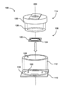
Fig. 3 is an exploded view of a representative one of camera modules 100,
which are
assembled on substrate sheet 116. Although, conventional camera modules are
manufactured
by coupling image capture device 108 to circuit substrate 110 before the
housing attach
process, camera module 100 is assembled by attaching image capture devices 108
to circuit
substrate 110 after housings 112 are formed on circuit substrate sheet 116.
This method is
particularly advantageous, because it minimizes the risks of damaging or
contaminating
image capture devices 108 during the prOcess of attaching housing 112 to
circuit substrate
110. As used herein, the term attaching is understood to include and means
ofjoining
housing 112 with substrate 110, including, but not limited to, forming or
molding housing
112 directly on circuit substrate 110 and attaching a preformed housing 112 to
circuit
substrate 110.
In this particular embodiment, each image capture device 108 (Fig. 3) is
mounted
through the central opening of one of housings 112, mechanically fixed (e.g.,
by an adhesive)
to the associated circuit substrate 110, and electrically coupled to the
circuitry of circuit
substrate 110. Circuit substrate 110 includes a top surface 118 whereon a
plurality of
electrical contacts 120 are formed. Contacts 120 facilitate the electrical
connection between
image capture device 108 and the circuitry of circuit substrate 110. Image
capture device 108
includes a corresponding set of electrical contacts 122 that are electrically
coupled to contacts
120 by some suitable means (e.g., wire bonding shown in Fig. 4).
5
CA 02654422 2008-11-27
WO 2007/143134
PCT/US2007/013014
It should be noted that contacts 122 need not be formed on the upper surface
of image
capture device 108 in order to provide for a .sufficient electrical connection
to circuit substrate
110. For example, image capture device 108 can include a plurality of contacts
formed on
it's rear surface such that image capture device 108 can be electrically
coupled to
corresponding contacts 122 of circuit substrate 110 via a solder process,
thereby mechanically
and electrically coupling image capture device 108 to circuit substrate 112 in
a single process.
Image capture device 108 further includes an image capture surface 124 on
which
images are focused by lens unit 114. What ever particular process is used,
image capture
device 108 should be mounted so that surface 124 remains substantially
perpendicular to
optical axis 200, so that surface 124 will lie in the focal plane of lens unit
114.
After image capture device 108 is attached, a lens unit 114 is positioned in
each
housing 112. The position of lens unit 114 within housing 112 is adjustable to
facilitate the
focusing of lens unit 114 with respect to image capture device 108. Housing
112 defines a
bore 126 that accepts lens barrel 128 of lens unit 114 and facilitates the
rotation of lens unit
114 about optical axis 200. Various mechanical adjustment means are known in
the art that
convert the rotational motion of lens unit 114 into translational motion along
optical axis 200.
However, no particular adjustment mechanism is shown, because the details of
the adjustment
mechanism, or even the inclusion of a focus mechanism, are not particularly
relevant to the
present invention. Lens unit 114 further includes a flange 130 that limits the
vertical
displacement of lens unit 114 with respect to housing 112 so that lens unit
cannot contact and
damage image capture device 108.
Fig.4 shows a cross-sectional view of fully assembled camera module 100.
Contacts
120 of circuit substrate 110 are electrically coupled to corresponding
contacts 122 of image
capture device 108 via a plurality of wire bonds 132. Lens unit 114 is shown
to include a
plurality of lenses 134 and an optical filter 136 (e.g., an infrared filter).
The details of lens
unit 114 and the particular optical elements contained therein are not
particularly relevant to
the present invention.
Fig. 5 is a top view of camera module 100 with lens unit 114 removed. Note
that the
diameter of bore 126 is greater than the diagonal of image capture device 108
so that image
capture device 108 can be mounted to circuit substrate 110 after housing 114
is formed
thereon. Optionally, the diameter of bore 126 can be nearly the same size as
the diagonal of
image capture device 108 to provide an easy means for positioning image
capture 108.
Fig 6. is an exploded view of an alternative camera module 600 including an
image
capture device 602, a circuit substrate 604, a housing 606, and a lens unit
608. In this
6
CA 02654422 2014-06-17
particular embodiment, circuit substrate 604 includes an aperture 610 that
allows light to
travel through a portion of circuit substrate 604. Aperture 610 is large
enough to allow lens
unit 608 to focus an image onto image capture surface 612 of image capture
device 602,
through aperture 610.
In this embodiment, image capture device 602 is flip-chip bonded to the bottom
surface of substrate 604 after housing 606 is formed/mounted on substrate 604.
In this flip-
chip bonding method, electrical contacts 614 of image capture device 602 are
bonded to
electrical contacts (not shown) on the bottom surface of circuit subst ate
604. Except as
explained below, the structure and assembly of housing 606 and lens unit 608
are
substantially the same as housing 112 and lens unit 114, respectively, as
described above.
Mount image capture device 602 to the bottom surface of circuit substrate 604
provides several advantages. For example, because image capture device 602 is
not mounted
through bore 616 (as in camera module 100), housing 606 and lens unit 608 can
be
significantly smaller. Note that the diameter of bore 616 is only slightly
larger than aperture
610, which is about the same size as image capture surface 612. Thus, the
overall footprint of
camera module 600 is significantly reduced. Another advantage is that even
though housing
606 is attached to circuit substrate 604 prior to Attaching image capture
device 602, housing
606 does not get in the way when attaching image capture device 602. In fact,
housing 606
provides extra support for circuit substrate 604 during the attachment of
image capture device
602, thereby making the attachment process more efficient and more reliable.
Fig. 7 shows a cross-sectional side view of camera module 600. In this
particular
embodiment, circuit substrate 604 includes a plurality of conductive traces
700 formed on the
rear surface. Traces 700 provide contacts for electrically connecting image
capture device
602 to circuit substrate 604 and also for electrically connecting circuit
substrate 604, and thus
image capture device 602, to another device such as host device PCB (Fig. 1).
The connections between contacts 614 of image capture device 602 and traces
700 of
circuit substrate 604 are made by gold-stud-bump, thermocompression bonding. A
plurality
of bumps 702 (e.g., au stud bumps) are formed on contacts 614. Image capture
device 602 is
then positioned on circuit substrate 604 so that the gold bumps 702 contact
traces 700. Then,
bonded connections are formed between gold bumps 702 and traces 700 and
contacts 614 by
applying heat and pressure. Optionally, nonconductive paste (NCP) 706 can be
applied
between image capture device 602 and circuit substrate 604 as part of the
bonding process to
further strengthen the bonded connections.
7
CA 02654422 2008-11-27
WO 2007/143134
PCT/US2007/013014
Note that the drawing of Fig. 7 is not to scale. For example, the relative
sizes of the
features are not accurately shown. Instead, certain features are exaggerated
to show the
detailed structure thereof.
Fig. 8 is a flow chart summarizing one method for manufacturing a camera
module
according to the present invention. In a first step 802, a circuit substrate
is provided. Next, in
a second step 804, an image capture device is provided. Then, in a third step
806, a lens unit
is provided. Next, in a fourth step 808, a lens housing is mounted on the
circuit substrate. As
used herein the term "mount" includes, but is not limited to, forming a
housing directly on the
circuit substrate (e.g., via a molding process) as well as attaching a
preformed housing. Then,
in a fourth step 810, the image capture device is mounted to the circuit
substrate after the
housing has been mounted. Finally, in a fifth step 812, the lens unit is
coupled to the
housing.
The description of particular embodiments of the present invention is now
complete.
Many of the described features may be substituted, altered or omitted without
departing from
the scope of the invention. For example, alternate lens units and housings,
may be substituted
for the lens units and housing shown. As another example, other processes
(e.g., thermosonic
bonding) can be used to mount the imagers to the circuit substrates. These and
other
deviations from the particular embodiments shown will be apparent to those
skilled in the art,
particularly in view of the foregoing disclosure.
=
8