Note: Descriptions are shown in the official language in which they were submitted.
CA 02654878 2008-12-10
Case 2573
GS
METHOD OF MANUFACTURING CARDS THAT EACH INCLUDE
AN ELECTRONIC MODULE AND INTERMEDIATE PRODUCTS
The present invention concerns a method of manufacturing cards
that each include an electronic module, in particular, an electronic module
comprising an electronic display. Preferably, the card obtained via the
method according to the invention is a bank card, in particular, conforming
to the ISO standard. However, the present invention can also apply to
electronic cards whose general profile is not rectangular, particularly
circular
cards. The present invention also concerns intermediate products obtained
within the scope of the method according to the invention.
Electronic cards or integrated circuit cards have considerably
developed over the last few years. Initially, electronic cards were formed of
a card body including a resistive contact module housed in a recess in the
body of the card. Then, contactless cards were made, i.e. cards including a
transponder formed of an electronic circuit connected to an antenna. As
electronic cards have developed, it is sought to integrate other electronic
elements for other functions into the cards. By way of example, cards
including a switch that can be activated by the user and an electronic
display have been disclosed. Such cards generally require relatively large
batteries or powering means of the photovoltaic cell type. In order to
integrate these various elements in a card, they are generally grouped
together in the form of at least one electronic module, including a support,
on the surface of which various electronic elements are arranged. Figure 1
shows a schematic example of this type of module. Module 2 includes an
integrated circuit 4, connected to an electronic display 6, a battery 8 and an
activator 10, arranged on a support or substrate 12, forming a PCB
interconnecting these various elements. In order to limit the thickness of
CA 02654878 2008-12-10
, A ,
- 2 -
these modules, the battery and/or the display can be arranged at the
periphery of support 12 or in recesses therein.
It is not easy to integrate a relatively large electronic module, made
up of various elements of variable shape and size, in a card. Further,
integrating a digital display, which has to be precisely positioned in the
manufactured card, causes an additional problem, which the present
invention proposes to overcome.
EP Patent No. 0 570 784 discloses, in one implementation, a method
of manufacturing cards including an electronic unit, in particular, a
transponder, which is placed in a main aperture in a positioning frame.
According to the implementation disclosed, the transponder and the
positioning frame are embedded in a binding agent that can be added in
liquid viscous form, particularly a resin. The positioning frame in EP Patent
No. 0 570 784 is used only for delimiting an inner zone for the transponder,
formed of an integrated circuit and a coil, inside the card. Thus, when
pressure is applied to the various elements and the binding agent to form a
card, the transponder is held in an inner zone, whereas it is possible for the
binding agent, in a non-solid state, to flow to form a layer that passes
through the manufactured card. Those skilled in the art can find, in this
Patent document, a method for integrating a relatively large and complex-
shaped electronic module in a compact, flat card. However, the electronic
module placed in the main aperture in a positioning frame, as described in
that document, will often be moved slightly when the card is being formed.
Indeed, this document does not disclose how to maintain the transponder in
a precise, determined position inside the aperture in the positioning frame.
Those skilled in the art might certainly think of reducing the dimensions of
the main aperture to make them approximately match the dimensions of the
electronic module, in particular the external profile of the module. However,
manufacturing tolerances must be taken into account, so that it is difficult
to
envisage too tight a fit. Moreover, depending upon the way in which the
modules are manufactured, the positioning of the various elements on the
CA 02654878 2008-12-10
- 3 -
support may also vary slightly. Thus, for example, digital display 6 is
arranged on the surface of the PCB or at the periphery thereof in a position
that may vary slightly. However, to obtain a high quality card, this digital
display must be positioned precisely relative to the external contour of the
manufactured card. This is particular important when a transparent
aperture, which fits the dimensions of the digital display, is arranged above
the aperture to allow the user of the card to read the display.
There is a further problem in addition to this problem of positioning
the electronic module relative to the external contour of the card. This
problem concerns introduction of the electronic module at the centre of the
card manufacturing installation. It will be noted here that electronic cards
are generally manufactured in batches, i.e. several cards are manufactured
simultaneously in the form of a plate that includes a plurality of electronic
modules. Then, each card is separated from the plate during a cutting step,
as is described in EP Patent No. 0 570 784. Within the scope of the latter
disclosure, the transponder remains free in relation to the positioning frame
until the card is formed. This requires precautions in the handling of the
various elements provided to form the card, to ensure that the transponders
remain in the corresponding apertures of the positioning structure until the
press is activated.
The present invention thus also proposes to answer this latter
problem, identified within the scope of the present invention, so as to
simplify the provision of electronic modules while ensuring that the
electronic modules are kept in the apertures of a positioning structure and
to facilitate assembly of the various elements and materials provided for
manufacturing the cards.
The present invention concerns generally a method of manufacturing
at least one card, each card including an electronic module. The method
provides for the provision of a frame or a plat having at least one aperture
arranged for receiving at least this electronic module. This method is
characterized in that at least one part of the peripheral area of said at
least
CA 02654878 2008-12-10
- 4 -
one aperture is deformed or crushed by the application of pressure,
localised at this at least one part of the peripheral area, on said frame or
said plate, so as to reduce locally the thickness of said frame or said plate
in said at least one part of the peripheral area, in that said electronic
module is brought opposite said at least one aperture, such that at least
one zone of the electronic module is superposed on said at least one part
of the peripheral area, and in that a material connection (i.e. a solid or
rigid
connection) is established between said at least one zone of said peripheral
area of said frame or said plate and said at least one zone of the electronic
module, before a resin is added to at least one side of said electronic
module in a subsequent step of the method.
It will be noted that the card obtained via the method according to the
invention can have several independent or electrically connected electronic
units, which may be in a single aperture in a frame or in several apertures of
a plate during the manufacturing process. In particular, a first unit is a
digital
display; a second unit is an electronic circuit and a third unit is a battery.
These units can be arranged on the same support and together form the
same module. However, some elements can have their own support or form
a distinct unit connected to the elements only by the electrical connection
wires or lugs. The various elements or units of an electronic module can be
bare, or separately coated embedded, or have a common coating.
It should be noted that the resin could be added in various forms and
in various states. The term "resin" should be understood in a broad sense,
including various known adhesives, PVC and Polyurethane resins or other
resins available to those skilled in the art.
In a first main implementation, the method according to the invention
is characterized in that said localised application of pressure is carried out
using a tool or a press before said electronic module is brought opposite
said at least one corresponding aperture, said at least one deformed or
crushed part defining at least one step on which said at least one zone of
the electronic module is then placed.
CA 02654878 2008-12-10
- 5 -
In a second main implementation, the method according to the
invention is characterized in that said electronic module is brought opposite
said at least one corresponding aperture prior to said localised application
of pressure, said at least one zone of the electronic module being then
pressed against said at least one part of said peripheral area so as to crush
or deform said at least one part and thus cause said electronic module to
move at least slightly more deeply into said at least one aperture.
The parts of said peripheral area of the frame or plate that will be
deformed or crushed can be formed of various materials and have different
structures. Conventional PVC or softer PVC, which will deform more easily
under the application of said pressure, can be used. A compressible
material can also be used, for example a slightly expanded synthetic or
natural material, which will be crushed locally by applying said pressure.
In a particular variant, the electronic module or the set of electrically
connected electronic modules, is located in several apertures separated by
one or more bridges provided between the various elements or units of one
module. The material connection between the plate and the module,
respectively modules, can then be provided at this or these bridge(s).
As a result of the features of the invention, the electronic module of
each card is held in a determined position in at least one aperture in the
frame or plate, owing to the material connection generated between said at
least one zone of the electronic module and said at least one part of the
peripheral area of said at least one aperture.
By selecting materials that adhere to each other, either by applying
pressure, with or without the addition of heat used to melt at least partially
one material or the other, or by adding adhesive between said at least one
zone and said at least one part, the electronic module is sufficiently
anchored in the frame to ensure that the module is held in a determined
position. It is thus possible easily to transport and move a plate forming a
skeleton for several cards with the electronic modules housed in a plurality
of apertures, which greatly facilitates the provision of these elements in the
CA 02654878 2008-12-10
- 6 -
card manufacturing installation. Moreover, at least partially fixing the edge
of the module to the peripheral area of the corresponding aperture also
ensures that the electronic module is held in position in the frame aperture
during the entire card manufacturing method according to the invention, in
particular when a resin is added.
Although the method according to the invention can already be
carried out with only one part of the peripheral area of the frame and one
corresponding zone of the edge of the electronic module, in a preferred
variant of the method according to the invention, the frame aperture has
first dimensions and a first profile and the electronic module has second
dimensions and a second profile, arranged such that at least two distinct
zones of the edge of the electronic module are superposed on two
corresponding parts of the peripheral area of the frame aperture, these two
zones and these two parts being respectively connected to each other and
ensuring that the electronic module is positioned precisely relative to the
frame.
According to a preferred variant of the invention, the electronic
module is substantially entirely located inside the frame aperture, the
thickness of the frame being greater than or approximately equal to the
maximum height of the electronic module. Preferably, the thickness of the
frame will be approximately adjusted to the maximum height of the
electronic module. Pressure is then applied to deform or crush said parts of
the frame, so that the electronic module is approximately located between
the top face and the bottom face of the frame, once the corresponding
zones of the module have been assembled to these parts of the frame.
The assembly formed of a plate with one or several apertures and
one or several electronic modules housed in said aperture(s) forms an
intermediate product according to the invention for manufacturing cards.
This unit is characterized in that each electronic module has at least one
zone materially connected to at least one part of the peripheral area of a
corresponding aperture in the plate, said at least one part of said peripheral
CA 02654878 2008-12-10
- 7 -
area being deformed or crushed by pressure and forming, jointly with said
at least one zone, a material connection between the electronic module and
said plate. It will be noted that at least one zone of the module and one
corresponding part of the plate can also have the additional function of
electrical connection between the module and a printed circuit on the plate.
It will be noted that in this text, the use of the terms "frame" or "plate"
is non-restrictive and not exclusive, unless the context clearly indicates so.
The assembly protected is generally formed by a plate pierced with
apertures and, in particular, by a frame. The term "frame" is used for the
particular case where the plate has a single aperture which houses at least
one electronic module. In other cases, where there are several apertures,
the term "plate" is generally used. Thus, particularly for a frame having a
single electronic module in one aperture, the plate forms a frame that may
be of varying width. However, when reference is made to an electronic
module in a corresponding aperture in a plate, this plate defines a
positioning frame for the module.
According to a preferred implementation of the invention, any resin or
binding agent forming a filling material is added to the remaining space in
the apertures in the plate of the aforementioned assembly, so that a full and
approximately flat structure is obtained. According to the invention, each
electronic module is thus materially connected to the frame or plate prior to
addition of the resin. The plate obtained according to this implementation
can form an intermediate product or a finished card. Various films can be
added on either side of this plate, particularly to form external layers of
the
card and/or printing films.
In a preferred variant, the contour of each card is achieved by a final
cutting operation, such that the previously described plate pierced with
apertures is cut and then at least partially forms the edge of the card in the
median zone. In another variant, the final cutting operation is carried out
inside the aperture such that the median part of the edge of the card is
essentially formed by the resin or filling material. In particular, if the
CA 02654878 2008-12-10
- 8 -
electronic module includes a support for the various elements, for example
a PCB, the cutting operation can also cut the substrate in an area close to
the edge thereof. In this case, the edge of the support partly defines the
edge of the resulting card.
Other advantages and particular features of the method according to
the present invention, and intermediate products obtained in preferred
implementations of the method, will appear more clearly upon reading the
following description. The description is made with reference to the
illustrative drawings, given by way of non-limiting example, in which:
- Figure 1, already described, shows schematically an electronic
module that can be integrated in a card according to the present invention;
- Figure 2 shows a first embodiment of a plate forming a plurality of
frames for the same number of cards manufactured in accordance with the
present invention;
- Figure 3 shows partially the plate of Figure 2, wherein two electronic
modules are located in apertures of the plate, at two different stages of the
method according to the invention;
- Figures 4 and 5 are cross-sections along the lines IV-IV and V-V of
Figure 3, showing respectively one step of a first main implementation of
the method according to the invention and a first embodiment of a plate and
electronic element assembly according to the invention;
- Figure 6 shows schematically a second embodiment of the plate
and electronic element assembly according to the invention;
- Figure 7 shows an implementation of the method of the invention
with the arrangement of several electronic modules in the same aperture in
a plate;
- Figures 8A and 8B each show an embodiment detail of the material
connection between an electronic module and the periphery of the aperture
in a plate;
CA 02654878 2008-12-10
- 9 -
- Figures 9A and 9B show two close variants of the first embodiment
of the plate and electronic module assembly;
- Figure 10 shows a third embodiment of the plate and electronic
module assembly for manufacturing a card according to the invention,
- Figure 11 shows schematically an alternative implementation of the
method of the invention with an electronic module arranged in two
apertures;
- Figures 12A to 120 show a second main implementation of the
method according to the invention;
- Figure 13 shows an embodiment of a plate forming a plurality of
frames for the same number of cards manufactured in accordance with the
second main implementation, in a configuration corresponding to the cross-
section of Figure 12b;
- Figure 14A shows another embodiment of a plate involved in the
manufacture of cards according to the second main implementation of the
invention, at the same stage as that shown in Figure 13;
- Figure 14B shows an embodiment of the plate and electronic
module assembly with the plate shown in Figure 14A;
- Figure 15 is a partial cross-section of a plate manufactured in
accordance with an implementation of the invention and forming several
cards. Figure 15 shows approximately in cross-section one area of this
plate corresponding to one card; the plate forming, in particular, an
intermediate product according to the invention;
- Figure 16 shows a cross-section of an additional step of a variant of
the first implementation of the method of the invention for obtaining finished
cards from the intermediate product of Figure 15; and
- Figure 17 shows schematically and in cross-section the formation of
a plate defining several cards, manufactured in accordance with a preferred
implementation of the method according to the invention.
CA 02654878 2008-12-10
- 10 -
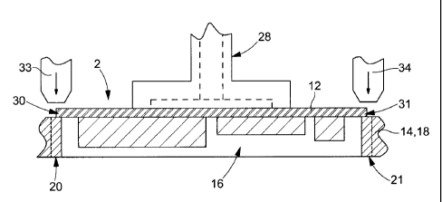
With reference to Figures 2 to 5, the initial steps of a first main
implementation of the method according to the invention, will now be
described. The manufactured cards include at least one electronic module
2, as shown schematically and solely by way of example in Figure 1, and a
frame 14, which has an aperture 16, arranged for receiving the electronic
module. Figure 2 shows a first embodiment of a plate 18 forming a plurality
of frames for a corresponding plurality of cards manufactured in accordance
with the invention. Plate 18 thus includes a plurality of through apertures 16
for receiving a corresponding plurality of electronic modules. The dotted
lines define the external contours of the manufactured cards, which are cut
along these dotted lines once the manufacturing method has been
performed for a plurality of cards in the form of a plate.
It will be noted that in Figure 2, the final cutting operation is
performed such that one frame 14 remains in the card and thus forms the
median part of the external edge of the card. In another variant, the final
cutting operation could be performed inside the aperture such that the
median part of the edge of the card is essentially formed by the filling
material in the aperture.
As shown in Figure 3, each through aperture 16 has first dimensions,
in particular a first width and a first length, and a first profile, which is
distinguished, by parts 20 and 21, which form two projecting portions
relative to the generally rectangular profile of aperture 16. These two parts
20, 21 are located in the peripheral area of aperture 16. Electronic module 2
has second dimensions, namely a second width and a second length, and a
second profile defined by the rectangular edge 24.
As shown in Figure 4, electronic module 2 is brought using picking or
gripping means 28, fitted with suction means, which generate an air
vacuum, opposite aperture 16 of frame 14. According to a first embodiment
of the median plate and electronic module assembly described here, the
first dimensions and the first profile of an aperture 16 are provided such
that, compared to the second dimensions and second profile of an
= CA 02654878 2008-12-10
- 11 -
electronic module 2, at least two distinct zones 30 and 31 of the edge of this
electronic module are superposed on the corresponding two parts 20 and
21 of the peripheral area of aperture 16. Zones 30 and 31 are applied
against the respective parts 20 and 21 and are then pressed against each
other in order to deform parts 20 and 21.
Plate 18 is formed, for example, of PVC or any other suitable
material. In general, support 12 of electronic module 2 is formed by a PCB,
which is deformed at a higher temperature than that at which the material
forming plate 18 is deformed. However, in a particular embodiment, in
particular so as to ensure some flexibility for an electronic module 2 of
large
dimensions, support 12 can also be formed of a material that has some
suppleness or flexibility and that is deformed in a similar way to PVC.
According to the variant of the method described with reference to
Figure 4, zones 30 and 31 are pressed against parts 20 and 21 using
thermodes 33 and 34 for heating frame 14 locally in projecting parts 20 and
21 and causing the electronic module to move slightly deeper into aperture
16, until the module is substantially entirely inside aperture 16, as shown in
Figure 5. The thermo-compression performed using thermodes 33 and 34
thus enables support 12 to be introduced into aperture 16 so that module 2
is entirely located between the bottom surface 36 and the top surface 38 of
plate 18. Deformation by thermo-compression thus anchors module 2 to
frame 14.
Because of the pressure exerted on zones 30 and 31, these zones
are pushed or penetrate into the corresponding projecting parts 20 and 21.
An interface surface 40 is thus formed between support 12 and frame 14 in
the areas of projecting portions 20 and 21. As is clear from Figure 5, this
step of deforming projecting portions 20 and 21, when zones 30 and 31 of
module 2 penetrate these parts, enables the electronic module to be
positioned precisely in aperture 16 in relation to frame 14. This positioning
is firstly lateral and positions electronic display 6 precisely relative to
frame
14. The positioning obtained is also vertical since the deformed parts 20
CA 02654878 2008-12-10
- 12 -
and 21 define stop members not only on the edge of support 12, but also
against the bottom surface 42 of the support. The electronic module is thus
positioned in aperture 16 of frame 14 by the two zones 30 and 31, which
remain secured to parts 20 and 21, which are deformed so as to match the
contour of the two zones. This ensures, in particular, that the electronic
module does not leave its aperture during the handling of plate 18, which is
shown in Figure 2 and includes electronic modules 16 arranged in its
apertures 15 as is shown in Figure 5.
It will be noted that, according to a preferred implementation of the
method of the invention, aperture 16 and electronic module 2 are arranged
to allow a filling material to be introduced, particularly a resin, in the
remaining space in the aperture, after the electronic module has been
assembled to frame 14 or to a plate pierced with holes.
The implementation of the invention described here presents the
preferred case with several distinct zones on the edge of module 2
superposed on several respective projecting parts, leaving a slot along most
of the edge of the electronic module. However, an alternative
implementation with a single zone on the module edge superposed on a
single corresponding part of the peripheral area of aperture 16 can also be
envisaged within the scope of the present invention. This variant already
enjoys some of the advantages of the invention, in particular anchoring the
electronic module in the frame.
The adherence of interface surface 40 can be increased, if
necessary, by adding beforehand a thin film of adhesive over parts 20 and
21 or over the corresponding zones 30 and 31 on the side of the bottom
surface 42 of support 12.
According to other embodiments of the pierced plate and electronic
module assembly, parts 20 and 21 can be deformed without using heat.
According to an advantageous variant, at least parts 20 and 21 of each
frame 14 are formed of a material that can easily be plastically deformed. In
a variant, deformation is facilitated by the use of ultrasound. In another
CA 02654878 2008-12-10
- 13 -
variant, at least parts 20 and 21 are formed of a compressible material,
which is crushed by said zones of the electronic module when pressure is
applied.
Preferably, a picking or gripping tool 28 follows the movement of
thermodes 33 and 34 until module 2 has entirely penetrated aperture 16,
i.e. module 2 remains held by the tool during the step of deforming parts 20
and 21 by applying pressure. This guarantees very precise positioning of
module 2 and also keeps it in a horizontal position, i.e. with support 12
approximately parallel to the top surface 38 of plate 18. This latter feature
facilitates the integration of a module with electrical contacts, which is
electrically connected to the electronic module.
As Figure 5 shows, according to a preferred variant, the thickness of
frame 14 is approximately identical to the maximum height of electronic
module 2. This module is pushed into aperture 16 until the top surface 44 of
support 12 approximately merges with the top face 38 of frame 14. As is
particularly clear in Figure 3, the first dimensions of aperture 16 and the
second dimensions of electronic module 2 are such that a slot 48 remains
between edge 24 of the module and the edge of the aperture, along most of
the edge of the electronic module.
The electronic module is shown with a substrate onto one surface of
which the various electronic elements are mounted. However, one could
also have a module with paths or other electrical/electronic elements
located on both surfaces of the substrate. In this latter case, it is
advantageous to press the substrate against the projecting parts of the
frame and to deform said parts until the substrate has sufficiently
penetrated the aperture for the electronic module to be entirely inside the
aperture.
Figure 6 shows a second embodiment of the assembly of pierced
plate 18A and electronic modules 2A. Figure 6 shows a single aperture 16A
in a plate forming a plurality of frames as shown in Figure 2. The
dimensions of a finished card are represented schematically by the outer
= CA 02654878 2008-12-10
- 14 -
dotted line. A similar diagram is used in the subsequent Figures 9, 10 and
11. Aperture 16A has a rectangular profile without any projecting portions.
However, substrate 12A of module 2A has two zones 30A and 31A
respectively forming two projecting parts relative to the general external
profile of the module, i.e. relative to its rectangular profile. These two
zones
30A and 31A on the edge of the electronic module are respectively
superposed on two parts 20A and 21A in the peripheral area of aperture
16A. Electronic module 2A can be assembled to frame 14A in a similar
manner to the manufacturing method according to the invention described
above.
Figure 7 shows an alternative implementation of the method. This
implementation is distinguished by the fact that several electronic modules
2A are arranged in the same aperture 71 of a plate 70. Zones 30A and 31A
of support 12A are fixed to the peripheral area of aperture 71 as in the case
of Figure 6. The final cutting operation in aperture 71 completely removes
plate 70. It will be noted that the cutting operation crops the two projecting
portions 30A and 31A. A final cutting operation can also be provided for
cutting the edge of the support 12A on at least part of its periphery.
Figure 8A shows a particular feature for better securing projecting
zones 30A and 31A of support 12C of electronic module 2A to parts 20A
and 21A of the peripheral area of aperture 16A. Each zone 30A and 31A is
provided with a hole 80 which is partially penetrated by part 20A,
respectively part 21A, when said part is deformed by pressure in
accordance with the method of the invention described above. An
alternative embodiment is shown in Figure 8B for implementation in
accordance with Figure 3. Here, support 12D of electronic module 2 is
provided with a slot 82 in zones 30 and 31 superposed on projecting parts
20 and 21 of the frame or plate. When these projecting parts are deformed
by pressure in accordance with the aforementioned method, said parts
partially penetrate slots 82 and secure module 2 properly to the frame or
plate.
CA 02654878 2008-12-10
- 15 -
Figures 9A and 9B show two variants of the first embodiment of the
pierced plate and electronic module assembly. Plate 18B has apertures
16B of generally rectangular shape, but with the four truncated corners
defining four parts 20B, 21B, 50B and 51B of the peripheral area of an
aperture. Support 12 of module 2 has a rectangular profile and dimensions
such that the four corners 30B, 31B, 52B and 53B define four zones of
module 2 respectively superposed on the four truncated corners of aperture
16B. Once module 2 has been brought opposite aperture 16B and correctly
positioned relative to the frame, the four corners of support 12 are pressed
against the four parts 20B, 21B, 50B and 51B of the plate to deform said
parts in a similar manner to the method described above for assembling the
electronic modules to the plate. The truncated corners are thus deformed
and form stop members for support 12 along the two horizontal directions.
of aperture 16B and also along the vertical direction. The truncated corner
parts of aperture 16B are thus deformed so as to match the shape of the
corners of the module and thereby enable module 2 to be precisely and
stably positioned relative to plate 18B. A slot 48, relative to the lateral
walls
of aperture 16B, preferably remains along the four sides of module 2.
The variant of Figure 9B differs from that of Figure 9A only in that the
parts of the peripheral area of the aperture superposed on the four corners
of module 2 are formed by four projecting parts arranged in the four corners
of aperture 16B. Each of these projecting parts defines a projection in the
contour of aperture 16B.
Figure 10 concerns a third embodiment of the assembly of plate 18
and the electronic modules. Here, each aperture 16 and electronic module
2 both have a rectangular profile with no projecting parts. One dimension of
support 12 is larger than the corresponding dimension of aperture 16. Thus,
the two lateral zones 30C and 31C are defined by two opposite sides of the
edge of module 2. These two zones are respectively superposed on the
peripheral area of aperture 16 defining two edges 20C and 21C of
rectangular aperture 16. Thus, as in the two other embodiments described
= CA 02654878 2008-12-10
- 16 -
above, the two zones 300 and 310 are pressed against parts 20C and 210
to allow module 2 to move slightly deeper into aperture 16 and to assemble
module 2 to frame 14, respectively to plate 18, so that the module is
arranged substantially entirely inside aperture 16, i.e. between the top and
bottom surfaces of frame 14, as shown in Figure 5. Parts 20C and 21C are
preferably deformed by thermo-compression. However, as in the preceding
embodiments, one could envisage obtaining the deformation at ambient
temperature, depending upon the nature of the materials used, or by
crushing a compressible material.
In a particular variant, the edge of support 12 covers the peripheral
area of aperture 16 of frame 14 on the four sides of the aperture such that
support 12 entirely closes aperture 16 on the support side. In such case,
aperture 16 has to be a through aperture, so that a resin can be introduced
into the remaining space in the aperture from the frame side opposite the
side where support 12 is arranged.
It will be noted that the electronic modules partially fill the
corresponding apertures in the embodiments shown in the Figures. Thus,
the electronic modules are assembled to the pierced plate such that the air
contained in the apertures can be easily evacuated from one side or other
of the plate and also so as to allow a filling material to be introduced, in
particular a resin, into these apertures, at least from one of the two sides
of
the plate. Preferably, the profile of each aperture and/or electronic module
are arranged to leave passages or slots that pass through the assembly
according to the invention. Thus, any residual air in the apertures when the
resin is added can escape more easily and the resin can pass through the
plate when it is introduced into the apertures. This is advantageous for
several reasons. This prevents air pockets forming firstly when the
electronic modules are assembled to the pierced plate and later when the
resin is added to the remaining space in the apertures. This also prevents
the resin being compressed in the apertures and causing inner stresses
that could subsequently cause surface deformations in the finished card.
= CA 02654878 2008-12-10
-17-
Figure 11 shows a particular embodiment. The electronic module 3
includes the elements described in Figure 1. Between display 6 and the
other elements, support 12 has a free transverse zone. This zone is
superposed on a bridge 85 of plate 18, and the bridge separates two
apertures 16 and 17. Display 6 is introduced into aperture 17 whereas the
other elements are located in aperture 16. According to the method of the
invention, bridge 85 is pressed against the transverse zone of the support
so as to deform the bridge to reduce the thickness thereof and to assemble
module 3 to plate 18. According to the terminology used in the claims, it is
clear that bridge 85 also forms a part of the peripheral area of each
aperture 16, 17. The support is shown passing between the two apertures
provided for receiving module 3. However, it is possible to make the support
in two parts, respectively located in the two apertures. In this latter case,
the
material connection between module 3 and frame 18 can be obtained by
pressing bridge 85 against the electrical connection wires or lugs provided
between display 6 and the other part of module 3.
The assembly formed by a plate pierced with apertures and the
electronic module or modules connected to the plate forms, in any given
embodiment, an intermediate product according to the present invention.
With reference to Figures 12 to 14, a second main implementation of
the method according to the invention will be described below. According to
a first variant, described in Figures 12A to 12C, this second implementation
is different essentially in that at least one part 20, 21 of the peripheral
area
of each aperture 16 of plate 18, forming a plurality of frames 14 for the
same number of cards being manufactured, is deformed or crushed by
applying pressure using a tool or a press 72. The pressure is preferably
applied at approximately ambient temperature. At least one tongue 74, 76 is
thus obtained, which defines a step that forms said at least one part of the
peripheral area of aperture 16,
In a preferred variant, a film of adhesive 78 is deposited before said
application of pressure at least over projecting parts 20 and 21. The
= CA 02654878 2008-12-10
- 18 -
material for the adhesive is chosen so that it spreads when parts 20 and 21
are deformed.
Next, an electronic module 2B is brought into aperture 16 so that
zones 80 and 82 of the edge of the module are superposed on the
corresponding preformed tongues 74 and 76. Module 2B differs from the
previously described module 2 in that its substrate 12B is thicker and a
recess is provided in the substrate for arranging display 6. A similar
arrangement can also be provided for the battery. Using a picking or
gripping tool 28, module 2B is positioned in aperture 16. Thermodes 33 and
34 are provided for heating the adhesive film 78 slightly so as to ensure that
zones 80 and 82 adhere well to tongues 74 and 76. However, it will be
noted that other types of adhesive that do not require heat could be used.
UV adhesives could be mentioned for example. As for the other
embodiments described, previously, once assembled, plate 18 and
modules 2B form a unit that defines an intermediate product according to
the invention.
According to another variant of the second implementation shown in
Figures 14A and 14B, plate 18A has parts 84 and 86 in the peripheral area
of each aperture 16A, which are crushed or deformed by the application of
pressure in similar manner to the first variant. Once deformed or crushed,
parts 84 and 86, form notches at the periphery of apertures 16A. Once
these notches have been pre-formed, modules 2A, with projecting zones or
tongues 30A and 31A that were described in Figure 6, are brought in a
similar manner to the first variant in apertures 16A. Zones 30A and 31A are
then placed in the corresponding notches 84 and 86. Again, an adhesive
film can be provided at the surface of the notches or tongues 30A and 31A.
The notches preferably have larger dimensions than the tongues of the
module so as to allow the module to be positioned precisely when it is
placed in the aperture. However, in another variant, the dimensions could
be adjusted, so that the notches are used for properly positioning the
module relative to frame 18A. When plate 18A and modules 2A are
= CA 02654878 2008-12-10
- 19 -
assembled to each other, they also form a unit that defines an intermediate
product according to the invention.
Both tongues 74, 76 and notches 84, 86 define a step with a smaller
thickness than that of the plate in which they are formed. All of the variants
described within the scope of the first main implementation of the method
according to the invention can apply by analogy to the second main
implementation described above.
According to a preferred implementation of the method according to
the invention, once the assembly of the plate and electronic modules has
been formed, a resin 60 is added to fill at least the remaining space in the
apertures. In the variant of Figure 15, the added resin forms a layer whose
thickness is greater than the height of the frame 14. The top and bottom
surfaces 36 and 38 are thus coated with a thin resin film 60. This resin also
fills slot 48 and thus forms an adherence interface between frame 14 and
the edge of support 12. Since said electronic module includes an electronic
display 6, resin 60 is transparent, at least in the area located above display
6.
Resin layer 60 can be formed by any technique known to those
skilled in the art, in particular by injection moulding, using a press or at
least
a laminating roller. In general, this resin is added after a plurality of
electronic modules have been arranged in a plurality of corresponding
apertures in a plate defining a plurality of frames for batch manufactured
cards.
Resin 60 can be formed by any appropriate material, particularly a
polyurethane resin, an epoxy resin, hotmelt adhesive melted by adding
heat, thermosetting materials, or even resin that hardens by ultraviolet
exposure or in the presence of humidity. Resin means any filling material
and any binding agent known to those skilled in the art and suitable for
manufacturing cards.
= CA 02654878 2008-12-10
- 20 -
The flat plate 62 obtained after the resin has solidified, as shown
partially in Figure 15, can form either a finished product, after the cards
have been cut out of the plate, or an intermediate product with flat surfaces.
It will be noted that the full plate 62, before the cards are cut out, forms
an
intermediate product that can be used subsequently in the manufacture of
cards with external layers or films added on either side of plate 62, as
shown in Figure 16. It is also possible to cut plate 62 to obtain a plurality
of
intermediate products with approximately the dimensions of a card. In this
latter case, the external layers are added card by card. Figure 16 simply
shows the addition of two solid layers 64 and 66 on each side of flat plate
62. These external layers 64 and 66 can be added and assembled to the
intermediate product 62 by conventional lamination or bonding. Preferably,
the cards are cut out of the plate obtained after the step shown in Figure 16.
In another variant, the added resin approximately fills the volume
remaining in aperture 16 without covering the top surface and the bottom
surface of the frame or the plate. In this case, the resin can be added only
to the side of the electronic module that is opposite the substrate. When flat
layer 62 is formed, those skilled in the art can provide sheets that do not
adhere, or barely adhere, on each side or on a single side of the product
shown in Figure 15, to prevent the resin from adhering to the press or
rollers during the manufacturing process. These sheets can also protect the
product during subsequent handling or transport to a plant for finishing the
card. In the case of a finished product, these sheets guarantee protection of
the surface prior to printing or sale. They are thus eventually removed.
Finally, Figure 17 shows schematically an implementation according
to the invention wherein a full, flat plate is formed, using laminating
rollers
68 and 69, by pressing resin 60, which is still in a viscous state, and two
external layers 64 and 66 to manufacture a full plate forming a plurality of
cards. This full plate has a central layer, formed by a resin 60 comprising
frame 14 and electronic modules 2, and two external layers on either side of
the central layer. After the resin has solidified, the full plate can be cut
into
CA 02654878 2008-12-10
- 21 -
the bank card format. However, it will be noted that other films could also be
added in a subsequent step.
It will be noted that resin 60 is preferably added in two steps. A first
part is deposited on the bottom layer 66 and a second part is deposited on
the assembly formed by plate 18 and electronic modules 2, as shown
schematically in Figure 17.
It will be noted that, when the resin is added, and in particular during
the laminating step described schematically in Figure 17, electronic
modules 2 are perfectly positioned relative to the apertures in frame 18 and
they are held in this position despite the pressure exerted by rollers 68 and
69. Other pressing means could evidently be envisaged by those skilled in
the art. As mentioned above, in a variant, the external layers 64 and 66
could be work sheets that are subsequently removed. In such case, these
external layers do not adhere to resin 60.