Note: Descriptions are shown in the official language in which they were submitted.
CA 02655051 2008-11-26
DESCRIPTION
ELECTRIC POWER CONVERTER
Technical Field
[0001]
The present invention relates to an electric power converter
provided with an inverter circuit that converts DC power supplied
to the input thereof into AC power and supplies the AC power to
a load connected to the output thereof.
Background Art
[0002]
To date, electric power converters provided with an inverter
circuit configured with semiconductor switching devices have been
utilized in a great number of industrial fields such as the electric
vehicle industry and the automobile industry. For example, there
exists an electric power converter (e. g. , refer to Patent Document
1) that is mounted in an electric vehicle and provided with an
inverter circuit whose input is connected to an overhead line via
a power collector and whose output is connected to a main motor
that drives the electric vehicle; cores formed of a
noise-suppression magnetic material are provided around the input
conductors and around the output conductors of the inverter circuit.
[0003]
Additionally, there exists an electric powerconverter(e.g.,
1
CA 02655051 2008-11-26
refer to Patent Document 2) that is mounted in an electric vehicle
and in which a voltage detector is connected to the input of an
inverter circuit and a current detector is connected to the output
of the inverter circuit, and based on a voltage detection signal
and a current detection signal from the detectors, the inverter
circuit is controlled.
[0004]
[Patent Document 1] Japanese Patent Application Laid-Open
No. 2004-187368
[Patent Document 2] Japanese Patent No. 3747858
Disclosure of the Invention
Problems to be Solved by the Invention
[0005]
In recent years, the operating voltage of a microcomputer
incorporated in a control unit of an electric power converter has
been lowered in order to reduce power consumption due to high-speed
processing. In the past, approximately 5-volt microcomputers were
utilized; however, in recent years, approximatelyl-volt to 3-volt
low-voltage-operation microcomputers have been utilized.
Accordingly, in order to prevent erroneous operation of a control
unit and to realize stable operation of an electric power converter,
it is required to suppress a common-mode noise current in the control
unit.
[0006]
2
CA 02655051 2008-11-26
It is conceivable that, in order to effectively suppress a
c.ommon-mode noise current in a control unit, there are takenmeasures
such as increasing the impedances, against the common-mode noise
current, of the voltage detector and the current detector provided
at the input side and the output side of an inverter circuit and
increasing the impedance of an insulated amplifier disposed at
the input side of the control unit that controls the inverter circuit;
however, taking the foregoing measures causes enlargement of
components, increase in the number of components, a cost hike,
and the like.
[0007]
The obj ective of the present invention is to obtain an electric
power converter that can ensure stable operation, even in the case
where there is utilized, for example, a microcomputer that
suppresses a common-mode noise current in a control unit, without
causing enlargement of components, increase in the number of
components, a cost hike, and the like, and operates with a relatively
low voltage.
Means for Solving the Problems
[0008]
An electric power converter according to the present invention
is provided with an inverter circuit that converts DC power supplied
to input terminals thereof into AC power and supplies the AC power
to a load connected with output terminals thereof, a capacitor
connected with the input terminal of the inverter circuit, a noise
3
CA 02655051 2008-11-26
suppression means that is provided around at least one of input-side
conductors connected with the input terminals of the inverter
circuit and output-side conductors connected with the output
terminals of the inverter circuit, an electric quantity detector
that is provided in the input-side conductors or the output-side
conductors at a position opposite to the inverter circuit with
respect to the noise suppression means, and a control unit that
controls the inverter circuit, based on an electric quantity
detection signal from the electric quantity detector.
Advantages of the Invention
[0009]
An electric power converter according to the present invention
can suppress a common-mode noise current in a control unit, without
causing enlargement of components, increase in the number of
components, a cost hike, and the like; therefore, the electric
power converter according to the present invention can ensure stable
operation even in the case where a microcomputer that operates
with a relatively low voltage is utilized.
Brief Description of the Drawings
[0010]
FIG. 1 is a block diagram illustrating an electric power
converter according to Embodiment 1 of the present invention;
FIG. 2 is a block diagram illustrating an electric power
converter according to Embodiment 2 of the present invention;
4
CA 02655051 2008-11-26
FIG. 3 is an explanatory diagram illustrating an equivalent
circuit for a common-mode noise current in an electric power
converter according to any one of Embodiments 1 and 2 of the present
invention;
FIG. 4 is a block diagram illustrating an electric power
converter according to technology 1 as a basis of the present
invention;
FIG. 5 is a block diagram illustrating an electric power
converter according to technology 2 as a basis of the present
invention; and
FIG. 6 is an explanatory diagram illustrating an equivalent
circuit for a common-mode noise current in an electric power
converter according to any one of technology 1 and technology 2
as bases of the present invention.
Description of Reference numerals
[0011]
1: OVERHEAD LINE
2: POWER COLLECTOR
3: REACTOR
4: WHEEL
5: RAIL
6: ELECTRIC POWER CONVERTER
7: THREE-PHASE AC S"1GTdR
10a: FIRST CORE
CA 02655051 2008-11-26
lOb: SECOND CORE
11: VOLTAGE DETECTOR
12: CAPACITOR
13a, 13b: INVERTER MODULE
SU, SV, SW, SX, SY, SZ: SWITCHING DEVICE
19a, 19b, 19c: CURRENT DETECTOR
20: CONTROL UNIT
22a, 22b, 22c, 22d: INSULATED AMPLIFIER
30: DISCHARGING RESISTOR
31: DISCHARGING DEVICE
Best Mode for Carrying Out the Invention
[0012]
Prior to explanations f or Embodiments of the present invention,
technologies as bases of the present invention will be explained.
[Technology 1 as Basis of the Present Invention]
[0013]
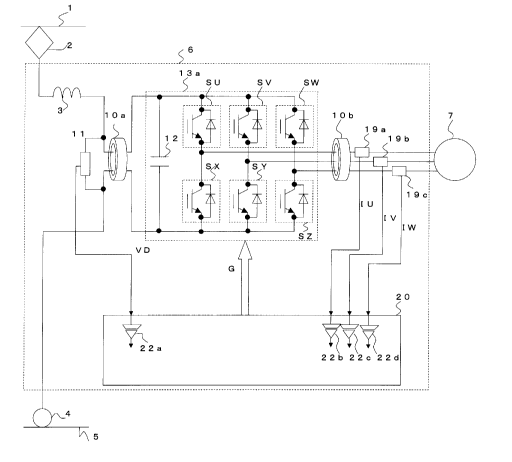
FIG. 4 is a block diagram illustrating an electric power
converter according to technology 1 as a basis of the present
invention; FIG. 4 illustrates an example of electric power converter
mounted in an electric vehicle. In FIG. 4, DC power is supplied
from an overhead line 1 to an electric power converter 6 mounted
in an electric vehicle, via a power collector 2. A switch
(unillustrated) and a smoothing circuit configured with a reactor
3 and a capacitor 12 are connected to the power collector 2. An
6
CA 02655051 2008-11-26
inverter module 13b as an inverter circuit is provided with a
three-phase bridge circuit configured with switching devices SU,
SV, SW, SX, SY, and SZ; the DC-side terminals as the input side
of the inverter module 13b are connected across the capacitor 12,
and AC-side terminals for U-phase, V-phase, and W-phase as the
output side of the inverter module 13b are connected to respective
input terminals of a three-phase AC motor 7(referred to as a motor,
hereinafter) that drives an electric vehicle.
[0014]
A voltage detector 11 that detects a voltage across the
capacitor 12 is connected between the DC-side terminals of the
inverter module 13b; current detectors 19a, 19b, and 19c that detect
output currents for respective phases are connected to the AC-side
terminals of the inverter module 13b; the negative-pole terminal
out of the DC-side terminals of the inverter module 13b is connected
to a rail 5 via a wheel 4 of the electric vehicle. The inverter
module 13b converts DC power supplied'- from the capacitor 12 into
AC power and outputs the AC power to the motor 7. In addition,
when the electric vehicle is braked in a regenerative manner, the
inverter module 13b converts AC power generated by the motor 7
into DC power and outputs the DC power to the capacitor 12.
[0015]
A voltage detection signal VD from the voltage detector 11
that detects the voltage across the capacitor 12 and current
detection signals IU to IW from the current detectors 19a to 19c
7
CA 02655051 2008-11-26
that detect the currents at the output-side of the inverter module
13b are inputted to a control unit 20 via insulated amplifiers
22a, 22b, 22c, and 22d. The control unit 20 generates a gate signal
G, based on the foregoing signals and an unillustrated comrnand
inputted from the outside, and outputs the gate signal G to the
gates of the switching devices SU to SZ.
[0016]
The switching devices SU to SZ supply three-phase AC power,
which is controlled based on the gate signal and undergoes pulse
width modulation (referred to as PWM, hereinafter) control, to
the motor 7 so that the motor 7 is controlled to generate desired
torque. The control unit 20 incorporates a microcomputer (ref erred
to as a micon, hereinafter) and is controlled with software.
[0017]
A first core 10a, which is formed of a magnetic material such
as ferrite or amorphous metal and hollow, ring-shaped, is provided
at the DC side, i.e., at the input-side of the inverter module
13b; a pair of conductive leads at the DC-side of the inverter
module 13b penetrates the inner space of the first core 10a. A
second core lOb, which is formed of a magnetic material such as
ferrite or amorphous metal and hollow, ring-shaped, is provided
at the output-side of the inverter module 13b; conductive leads
for U-phase, V-phase, and W-phase at the output-side of the inverter
module 13b penetrate the inner space of the second core 10b.
[0018]
8
CA 02655051 2008-11-26
In practice, the first and second cores 10a and 10b are each
configured with a plurality of cores in series and have a relatively
large size. Accordingly, the first and second cores are not disposed
inside the inverter module 13b, but inside a metal case that has
a relatively large space and incorporates the electric power
converter 6 configured with the inverter module 13b, the control
unit 20, the capacitor 11, and the reactor 3. In addition, the
current detectors 19a to 19c and the voltage detector 11 are also
included in the metal case that incorporates the electric power
converter 6.
[0019]
The voltage detector 11 is connected between the input-side
conductors of the inverter module 13b, at the output side of the
first core 10a, i.e., at the inverter module 13b side of the first
core 10a. The current detectors 19a to 19c are disposed on the
output-side conductors of the inverter module 13b, at the input
side of the second core lOb, i. e. , at the inverter module 13b side
of the second core lOb.
[0020]
As described above, the current detection signals IU, IV,
and IW obtained from the current detectors 19a to 19c are utilized
for controlling the motor 7; also in the case where an abnormality
such as a short circuit or a short-to-ground fault occurs at the
AC-side terminals, i.e., at the output-side conductors of the
inverter module 13b, the current detection signals IU, IV, and
9
CA 02655051 2008-11-26
IW are utilized for performing protective operation, by securely
detecting the abnormality and making the control unit 20 interrupt
the switching operations of the switching devices SU to SZ.
Accordingly, the current detectors 19a to 19c are disposed in the
vicinity of the switching devices SU to SZ inside the inverter
module 13b so that an abnormal current in the output line of the
inverter module 13b can be detected in as wide a range as possible.
Due to its function of detecting the voltage across the capacitor
12, the voltage detector 11 is disposed in the immediate vicinity
of the capacitor 12.
[0021]
The electric power converter 6 configured as described above
is characterized by having a large control capacity of approximately
1 [MVA] and a high circuit voltage of approximately 600 [V] to
3000 [V] ; thus, in the case where the switching devices SU to SZ
inside the inverter module 13b perform switching operations, the
voltage at the circuit in the vicinity of the switching devices
changes fromapproximately 0[V] to approximately 3000 [V] in several
microseconds. The voltage change causes a high-frequency leakage
current to occur through stray capacitances in the circuitry. The
leakage current outflows from and flows into the electric power
converter 6. A leakage current of this kind is referred to as a
common-mode noise current.
[0022]
In many cases, the electric power converter 6 is mounted under
CA 02655051 2008-11-26
the floor of a vehicle; when a common-mode noise current outflows
from the case of the electric power converter 6 to the vehicle
body, there is formed a large loop circuit in which the common-mode
noise current f lows; therefore, high-f requency magneticflux caused
by the common-mode noise current may adversely affect signal
apparatuses (unillustrated) installed in the vicinity of a rail.
The first core 10a and the second core 10b in the electric power
converter 6 are provided in order to avoid the foregoing adverse
effect, and operate as noise suppression means that suppress the
outflow of a common-mode noise current.
[0023]
That is to say, as described above, the inner space of the
first core l0a is penetrated by a pair of conductors at the input-side
of the inverter module 13b, and the inner space of the second core
lOb is penetrated by three conductors at the output-side of the
inverter module 13b. Therefore, the first core 10a and the second
core ].Ob each generate impedance against common-mode noise currents
that flow in a plurality of conductors that penetrate the respective
cores so as to suppress the common-mode noise currents. In general,
the first core 10a and the second lOb are each configured with
a plurality of cores in series, in order to fulfill the request
for reduction of a common-mode noise current.
[0024]
[Technology 2 as Basis of the Present Invention]
FIG. 5 is a block diagram illustrating an electric power
11
CA 02655051 2008-11-26
converter according to technology 2 as a basis of the present
invention. In FIG. 5, a discharging resistor 30 and a discharging
device 31 are connected in series and configure an
overvoltage-suppression discharging circuit. The
overvoltage-suppression discharging circuit is connected in
parallel with the capacitor 12. The voltage detector 11 is connected
across the discharging device 31. Other configurations are the
same as those in technology 1 as a basis of the present invention.
[0025]
In the case where the voltage across the capacitor 12 becomes
excessively high, the overvoltage-suppression discharging circuit
configured with the discharging resistor 30 and the discharging
device 31 makes the discharging device 31 turn on so as to discharge
electric charges on the capacitor 12 through the discharging
resistor 30. As a result, the inverter module 13b can be prevented
from being broken by the overvoltage.
[0026]
The reason why the voltage detector 11 is connected across
the discharging device 31 is that the voltage detector 11 has not
only a function of detecting the voltage across the capacitor 12
but also a function of ascertaining the operation of the discharging
device 31. In a normal condition (when the discharging device is
off), the foregoing configuration enables the voltage detector
11 to detect the voltage across the capacitor 12, and upon the
occurrence of an overvoltage (when the discharging device turns
12
CA 02655051 2008-11-26
on) , the detection value of the voltage detector 11 becomes zero,
whereby the control unit 20 can be aware of the fact that the
discharging device 31 has turned on; therefore, it is made possible
to monitor whether or not the discharging device31operatesnormally_
In addition, because the inverter module 13b is interrupted when
an overvoltage occurs, no problem in the controlling operation
is posed even though the detection value of the voltage detector
11 becomes zero.
[0027]
FIG. 6 is an explanatory diagram illustrating an equivalent
circuit for a common-mode noise current in any one of technology
1 and technology 2, illustrated in FIGS. 4 and 5, as bases of the
present invention. In addition, in order to comprehend the
phenomenon, the equivalent circuit illustrated in FIG. 6 is
represented in a simplified manner, without impairing the physical
significance. In FIG. 6, VN denotes a common-mode noise voltage
generated by a voltage change due to the switching operations of
the switching devices SU to SZ; as the paths of a common-mode noise
current generated by the common-mode noise voltage VN, four paths
Al, A2, Bl, and B2 are conceivable.
[0028]
(1) Path Al
The pathAl is formed of a series circuit including an impedance
ZlA between the switching devices SU to SZ and the first core 10a,
an impedance Z2A of the first core 10a, and an impedance Z3A of
13
CA 02655051 2008-11-26
a circuit whose route starts from the first core l0a and returns
to the source of common-mode noise via the outside of the electric
power converter 6 or the case of the electric power converter 6.
[0029]
(2) Path A2
The pathA2 is formed of a series circuit including an impedance
Z4A between the switching devices SU to SZ and the voltage detector
11, an impedance Z5A of the voltage detector 11, an impedance Z6A
of a circuit that starts from the voltage detector 11 and leads
to the control unit 20 via the insulated amplifier 22a, and an
impedance Z7A of a circuit that starts from the control unit 20
and returns to the source of common-mode noise via the case of
the electric power converter 6. In addition, because the distance
between the switching devices SU to SZ and the first core IOa is
longer than the distance between the switching devices SU to SZ
and the voltage detector 11, Z1A is larger than Z4A.
[0030]
(3) Path B1
The path B1 is formed of a series circuit including an impedance
Z1B between the switching devices SU to SZ and the second core
10b, an impedance Z2B of the second core lOb, and an impedance
Z3B of a circuit whose route starts from the second core 10b and
returns to the source of common-mode noise via the outside of the
electric power converter 6 or the case of the electric power converter
6.
14
CA 02655051 2008-11-26
[0031]
(4) Path B2
The path B2 is formed of a series circuit including an impedance
Z4B between the switching devices SU to SZ and the current detectors
19a to 19c, an impedance Z5B of the current detectors 19a to 19c,
an impedance Z6B of a circuit that starts from the current detectors
19a to 19c and leads to the control unit 20 via the insulated
amplifiers 22b to 22d, an impedance Z7B of a circuit that starts
from the control unit 20 and returns to the source of common-mode
noise via the case of the electric power converter 6. In addition,
because the distance between the switching devices SU to SZ and
the second core lOb is longer than the distance between the switching
devices SU to SZ and the current detectors 19a to 19c, ZlB is larger
than Z4B.
[0032]
As can be seen from FIG. 6, common-mode noise currents that
flow toward the outside of the electric power converter 6 through
the paths Al and Bl are suppressed by the impedances Z2A and Z2B
of the first and second cores 10a and lOb; therefore, the common-mode
noise currents are suppressed from widely flowing toward the vehicle
body or the like outside the electric power converter 6, whereby
the common-mode noise current is suppressed from flowing in a large
loop circuit. As a result, because high-frequency magnetic flux
generated by the common-mode noise current can be reduced, the
adverse effect thereof on signal apparatuses (unillustrated)
CA 02655051 2008-11-26
installed in the vicinity of a rail can be reduced.
[0033]
As described above, common-mode noise currents that flow
toward the outside of the electric power converter 6 through the
paths Al and B1 can be suppressed by the first and second cores
l0a and lOb; however, common-mode noise currents that flow in the
control unit 20 inside the electric power converter 6 through the
paths A2 and B2 cannot be suppressed. However, in order to prevent
erroneous operation of the control unit 20 so as to. ensure stable
operation of the electric power converter 6, it is indispensable
to suppress the common-mode noise currents that flow through the
paths A2 and B2.
[0034]
Accordingly, in order to increase the impedances Z5A and Z5B,
against common-mode noise currents, of the voltage detector 11
and the current detectors 19a to 19c, noise suppression means
(unillustrated) are provided in the voltage detector 11 or the
current detectors 19a to 19c, or the insulated amplifiers 22a to
22d are provided at the input side of the control unit 20 and are
made to function as impedances Z6A and Z6B, so that common-mode
noise currents that flow through the paths A2 and B2 are suppressed.
[0035]
Next, Embodiments of the present invention will be explained.
Embodiment 1
FIG. 1 is a block diagram illustrating an electric power
16
CA 02655051 2008-11-26
converter according to Embodiment 1 of the present invention;
constituent elements the same as or similar to those in the
technologies as bases of the present invention are designated by
the same reference characters.
[0036]
In foregoing technology 1 as a basis of the present invention,
the voltage detector 11 is connected between the input-side
conductors of the inverter module 13b, at the output side of the
first core 10a, i.e. , at the inverter module 13b side of the first
core 10a; however, as illustrated in FIG. 1, in an electric power
converter according to Embodiment 1 of the present invention, the
voltage detector 11 is connected between the input-side conductors
of the inverter module 13a, at the input side of the first core
10a, i.e., at a place opposite to the inverter module 13a with
respect to the first core 10a. The first core 10a has an impedance
only against a common-mode noise current; therefore, even though
the voltage detector 11 is connected between the input-side
conductors of the inverter module 13a, at the input side of the
first core 10a, i.e., at a place opposite to the inverter module
13a with respect to the first core 10a, the voltage across the
capacitor 12 can be detected.
[0037]
Additionally, in technology 1 as a basis of the present
invention, the current detectors 19a to 19c are disposed inside
the case of the inverter module 13b in such a way as to be on the
17
CA 02655051 2008-11-26
output-side conductors of the inverter module 13b, at the input
side of the second core 10b, i. e., at the inverter module 13b side
of the second core 10b; however, in an electric power converter
according to Embodiment 1 of the present invention, the current
detectors 19a to 19c are provided on the output-side conductors
of the inverter module 13a at the output side of the second core
10b, i.e., at a place opposite to the inverter module 13a with
respect to the second core 10b. The current detectors 19a to 19c
are disposed outside the inverter module 13a.
[0038]
The switching devices SU to SZ in Embodiment 1 are formed
of an intelligent power module (referred to an IPM, hereinafter)
or a power module integrated with a gate driver having an
excessive-current protection function.
[0039]
An IPM or a power module integrated with a gate driver having
an excessive-current protection function has a function of
detecting an excessive current due to short-circuiting or a
short-to-ground fault of the output conductor thereof and
automatically turning off switching operation; therefore, it is
not required to detect the excessive current through the current
sensors 19a to 19c and turn off the switching operation by the
intermediary of the control unit 20, whereby protective operation
against the excessive current can rapidly and securely be performed.
[0040]
18
CA 02655051 2008-11-26
Accordingly, although, in Embodiment 1 of the present
invention, the current sensors 19a to 19c are provided at the output
side, (the motor side) of the second core lOb, which is away from
the switching devices SU to SZ, it is made possible to protect
the switching devices SU to SZ, even though there occurs
short-circuiting or a short-to-ground fault of a wiring conductor
between the switching devices SU to SZ and the current sensors
19a to 19c. In other words, in the case where there occurs
short-circuiting or a short-to-ground fault at a position (near
to the switching devices SU to SZ) that is closer to the power
source than the current sensors 19a to 19c are, no current flows
in the current sensors 19a to 19c in the technology as a basis
of the present invention; therefore, because the current sensors
19a to 19c cannot detect short-circuiting, a short-to-ground f ault,
or the like, the switching devices cannot be turned off, whereby
the electric power converter is likely to break. However, in the
configuration according to Embodiment 1 of the present invention,
the switching devices SU to SZ themselves have an excessive-current
protection function; thus, it is made possible to turn off the
switching devices SU to SZ so as to avoid the breakage of the electric
power converter, even in the case where there occurs
short-circuiting or a short-to-ground fault of a wiring conductor
between the switching devices SU to SZ and the current sensors
19a to 19c.
[0041]
19
CA 02655051 2008-11-26
Embodiment 2
FIG. 2 is a block diagram illustrating an electric power
converter according to Embodiment 2 of the present invention. In
FIG. 2, the discharging resistor 30 and the discharging device
31 are connected in series and configure an overvoltage-suppression
discharging circuit. The overvoltage-suppression discharging
circuit is connected in parallelwith the capacitorl2. Thevoltage
detector 11 is connected across the discharging device 31.
[0042]
In foregoing technology 2 as a basis of the present invention,
the voltage detector 11 is disposed at the output side of the first
core 10a; however, as illustrated in FIG. 2, in an electric power
converter according to Embodiment 2 of the present invention, the
voltage detector 11 is disposed at the input side of the first
core 10a. The first core 10a has an impedance only against a
common-mode noise current; therefore, even though disposed at the
input side of the first core 10a, the voltage detector 11 can detect
the voltage across the capacitor 12.
[0043]
In technology 2 as a basis of the present invention, the current
detectors 19a to 19c are disposed at the input side of the second
core lOb and inside the case of the inverter module 13b; however,
in the electric power converter according to Embodiment 2 of the
present invention, the current detectors 19a to 19c are disposed
at the output side of the second core 10b and outside the inverter
CA 02655051 2008-11-26
modulel3a. Otherconfigurationsarethesame asthosein Embodiment
1.
[0044]
FIG. 3 is an explanatory diagram illustrating an equivalent
circuit for a common-mode noise current in an electric power
converter according to any one of Embodiments 1 and 2 of the present
invention. In addition, in order to comprehend the phenomenon,
the equivalent circuit illustrated in FIG. 3 is represented in
a simplified manner, without impairing the physical significance.
In FIG. 3, VN denotes a common-mode noise voltage generated by
a voltage change due to the switching operations of the switching
devices SU to SZ; as the paths of a common-mode noise current
generated by the common-mode noise voltage VN, four paths Al, A3,
Bl, and B3 are conceivable.
[0045]
Because the paths Al and Bl are the same as those in FIG.
6 explained in the technology as a basis of the present invention,
explanations therefor will be omitted. In Embodiments 1 and 2 of
the present invention, instead of the paths A2 and B2 in technology
1 and technology 2 as bases of the present invention, there are
provided the paths A3 and B3, respectively.
[0046]
(1) Path A3
The path A3 is formed of a series circuit including an impedance
ZlA between the switching devices SU to SZ and the first core 10a,
21
{ CA 02655051 2008-11-26
an impedance Z2A of the first core 10a, an impedance Z5A of the
voltage detector 11, an impedance Z6A of a circuit that starts
from the voltage detector 11 and leads to the control unit 20 via
the insulated amplifier 22a, and an impedance Z7A of a circuit
that starts from the control unit 20 and returns to the source
of common-mode noise via the case of the electric power converter
6.
[0047J
(2) Path B3
The path B3 is formed of a series circuit including an impedance
Z1B between the switching devices SU to SZ and the second core
IOb, an impedance Z2B of the second core 10b, an impedance Z5B
of the current detectors 19a to 19c, an impedance Z6B of a circuit
that starts from the current detectors 19a to 19c and leads to
the control unit 20 via the insulated amplifiers 22b to 22d, and
an impedance Z7B of a circuit that starts from the control unit
20 and returns to the source of common-mode noise via the case
of the electric power converter 6.
[0048]
In comparison with the paths A2 and B2 in technologies (in
FIG. 6) as based of the present invention, it can be seen that,
in the paths A3 and B3 in Embodiment 2 of the present invention,
the impedance Z4A of the circuit between the switching devices
SU to SZ and the voltage detector 11 becomes the impedance Z1A
of the circuit between the switching devices SU to SZ and the first
22
CA 02655051 2008-11-26
core l0a (Z1A > Z4A) , the impedance Z4B of the circuit between the
switching devices SU to SZ and the current detectors 19a to 19c
becomes the impedance Z1B of the circuit between the switching
devices SU to SZ and the second core lOb ( Z1B> Z4B) , and the impedance
Z2A of the first core 10a and the impedance Z2B of the second core
lOb are increased. That is to say, it can be seen that, in Embodiment
2 of the present invention, the first and second cores l0a and
10b, which are originally provided for suppressing a common-mode
noise current that flows toward the outside of the electric power
converter 6, can also suppress a common-mode noise current that
flows to the control unit 20.
[0049]
As described above, in an electric power converter according
to any one of Embodiments 1 and 2 of the present invention, the
voltage across the capacitor 12 can be detected; in the case where
there occurs an abnormality such as short-circuiting or a
short-to-ground fault of the conductors as the output lines of
the inverter module 13a, it is made possible to maintain an
excessive-current protection function of securely detecting the
abnormality and interrupting the switching operation; and a
common-mode noise current can be suppressed, without enlargement
of components, increase in the number of components, and a cost
hike being caused, e.g., by providing a noise suppression means
in the voltage detector 11 or the current detector 19a to 19c.
Therefore, there can be obtained an electric power converter that
23
CA 02655051 2008-11-26
can ensure stable operation even though a low-voltage-operation
microcomputer of these days is utilized.
[0050]
The configurations described in Embodiments 1 and 2 are
examples of the aspects of the present invention and can be combined
with other publicly known technologies; it goes without saying
that various features of the present invention can be configured,
by modifying, for example, partially omitting the foregoing
embodiments, without departing from the scope and spirit of the
present invention.
[0051]
For example, in Embodiments 1 and 2 of the present invention,
there has been explained an example in which a voltage detector
is disposed at the input side of an inverter module, and current
detectors are disposed at the output side of the inverter module;
however, it goes without saying that the current detectors may
be disposed at the input side of the inverter module, and the voltage
detector may be disposed at the output side of the inverter module.
Moreover, an electric quantity detector may be provided at a place
opposite to the inverter module with respect to only one of the
first core 10a and the second core lOb. Sti11 moreover, a switching
device having no excessive-current protection function may be
utilized.
[0052]
The present invention may be applied to an electric power
24
CA 02655051 2008-11-26
converter configured in such a way that AC power is supplied from
a power collector, the AC power is converted into DC power by a
converter, and then the DC power is inputted to an inverter module.
Additionally, it is also possible to apply the present invention
to a so-called auxiliary power source apparatus in which loads
such as a vehicle air conditioner and an illumination apparatus
are connected to the output terminal of an electric power converter
via devices other than a motor, e.g. , a transformer and a smoothing
circuit, and the electric power converter is operated with a constant
voltage and at a constant frequency so that constant-voltage and
constant-frequency power is supplied to the loads.
Industrial Applicability
[0053]
An electric power converter according to the present invention
can be applied not only to an electric vehicle but also to various
related fields such as fields of electric automobiles, elevators,
and electric systems.