Note: Descriptions are shown in the official language in which they were submitted.
CA 02655451 2008-12-15
WO 2007/144574 PCT/GB2007/002105
1
ELECTROMAGNETIC RADIATION ENHANCEMENT AND DECOUPLING
This invention relates devices which manipulate electromagnetic radiation (EM)
and
more specifically relates to the field of coupling energy into identification
devices such as
RF (radio frequency) tags. The invention allows the tag to be decoupled (i.e.
isolated)
from surfaces which degrade tag performance, such as metallic surfaces. The
invention
relates to any EM tag, particularly those that rely upon propagating wave
interactions (as
opposed to the inductive coupling exhibited by magnetic tags). Hence our
preferred
embodiment involves application to long-range system tags (e.g. UHF-range and
microwave-range tags).
Electronic devices which can transmit a modulated electromagnetic signal that
can be
detected by an appropriate reader are widely used for the identification and
tracking of
items, particularly for articles in a shop or warehouse environment. Such
devices, which
will be referred to throughout this specification as EM tags or simply as
tags, generally
comprise a chip coupled to an integral antenna which is tuned to a particular
frequency
of operation. The frequency of operation of current EM tags is generally radio
frequencies (RF), including the ultra high frequency (UHF) and microwave
ranges but the
present invention is applicable to a tag which operates at any frequency. The
tags may
be passive, in that they interact with incident radiation of the appropriate
frequency and
re-transmit a modulated signal back to a reader, or active in which the tag
contains its
own power source.
One commonly experienced disadvantage with such tags, especially passive tags,
is that
if directly placed on (or within a several millimetres of) a metal surface
their read range is
decreased to unacceptable levels and - more typically - the tag cannot be read
or
interrogated. This is because a propagating-wave RF tag uses an integral
antenna to
receive the incident radiation: the antenna's dimensions and geometry dictate
the
frequency at which it resonates, and hence tailor the frequency of operation
of the tag
(typically 866MHz or 915MHz for a UHF (ultra-high frequency) range tag and 2.4-
2.5
GHz or 5.8GHz for a microwave-range tag). When the tag is placed near or in
direct
contact with a metallic surface, the tag's conductive antenna interacts with
that surface,
and hence its resonant properties are degraded or - more typically - negated.
Therefore,
the tracking of metal articles such as cages or containers is very difficult
to achieve with
UHF RF tags and so other more expensive location systems have to be employed,
such
as GPS.
CA 02655451 2008-12-15
WO 2007/144574 PCT/GB2007/002105
2
UHF RFID tags also experience similar problems when applied to certain other
surfaces
which interact with RF (radio frequency) electromagnetic waves, such as,
certain types of
glass and surfaces which possess significant water content, examples including
certain
types of wood with a high water or sap content. Problems will also be
encountered when
tagging materials which contain/house water such as, for example, water
bottles, drinks
cans or human bodies etc.
One way around this problem is to place a foam spacer between the RF tag and
the
surface, preventing interaction of the antenna and the surface. With currently-
available
systems the foam spacer typically needs to be at least 10-15mm thick in order
to
physically distance the RF tag from the surface by a sufficient amount.
Clearly, a spacer
of this thickness is impractical for many applications and is prone to being
accidentally
knocked and damaged.
Other methods have involved the provision of unique patterned antennas which
have
been designed to impedance match a particular RF tag with a particular
environment.
For example, International patent application W02004/093249 to Avery Dennison
attempts to deal with this problem by using tags having antennas with
compensating
elements. The antenna is designed with surface effects in mind and is tuned to
a
particular environment or range of possible environments. This avoids the need
for a
large spacer but does require relatively complicated antenna designs which
must be
different for each tag, therefore adding to the cost and complexity of
manufacture.
US 5,995,048 describes an antenna design which minimises surface effects in
which a
quarter wave patch antenna is spaced apart from a much larger ground plane.
The
design does minimise surface reflection effects but the patch antenna is
preferably
spaced away from the ground plane by a distance equal to a quarter wavelength
which is
a large spacing and suffers from the same problems as for the foam spacer
mentioned
above. It also requires a large ground plane which may be not achievable in
all
circumstances. Further the patch antenna, which is a resonant circuit, must be
carefully
impedance matched to the tag resonating circuit in order to operate
effectively.
It is therefore an object of the invention to provide a mount for an EM tag
which acts as
an electromagnetic radiation decoupler material which mitigates at least some
of the
CA 02655451 2008-12-15
WO 2007/144574 PCT/GB2007/002105
3
problems associated with prior art systems, namely those of thickness, size
and
flexibility.
It is a further object of the invention to provide apparatus for coupling
incident energy into
an electronic device or tag, while at the same time isolating such coupling
effect from the
potentially adverse effects of a substrate on which the device or tag is
mounted.
Thus according to the present invention there is provided an electromagnetic
radiation
decoupler comprising a cavity structure which comprises a conducting base
portion
connected to a first conducting side wall and a second conducting side wall,
the first
conducting side wall and second conducting side wall being spaced apart and
substantially parallel. Preferably a dielectric material is disposed within
the cavity
structure.
Embodiments of the invention can therefore be very simple structures
comprising a
cavity structure formed by two, separate, parallel conducting surfaces each
connected to
a conducting base portion. The cavity itself is defined by the area of overlap
of the two
conducting side walls and the conducting end portion. Where the dielectric
material is a-
fluid such as a gas, for example, air, the solid structure of the cavity may
be defined only
by the conducting side walls and conducting base portion although there may be
some
solid spacers used to maintain the spacing of the side walls. Where the
dielectric
material is a solid the sides of the dielectric material may define non-
conducting side
walls of the cavity structure.
Embodiments according to this aspect of the invention can be thought of as
providing an
unusually thin sub-wavelength resonant cavity which is closed at one end.
Incident
radiation at the wavelength of interest couples into the dielectric material
and, at a
resonant frequency, forms standing waves. Where the cavity length, as defined
by the
area of overlap of the first conducting side wall with the second conducting
side wall, is a
quarter of the wavelength of the incident radiation (in the particular
dielectric material
used) a standing wave situation is created. The conducting base portion and
two wali
portions together create a continuous metal boundary around three sides of the
dielectric
core and force the electric field parallel to the surface of the base portion
to be a
minimum (or a node) at the base portion and therefore (since it is a quarter-
wavelength
long) at the opposite end of the cavity structure to the conducting base
portion the
electric field is at a maximum (antinode).
CA 02655451 2008-12-15
WO 2007/144574 PCT/GB2007/002105
4
This structure results in the strength of the electromagnetic fields in the
core being
resonantly enhanced: constructive interference between waves internally
reflected by the
base portion and those from the interrogating antenna coupled in through the
open end
of the cavity are superimposed resulting in field strengths of 50 or 100 times
greater than
that of the incident radiation. Advantageously, enhancement factors of 200 or
even 300
or more can be produced. In more specific applications typically involving
very small
devices, lower enhancement factors of 20,30 or 40 times may still result in a
readable
system which would not be possible without such enhancement. The fieid pattern
is such
that the electric field is strongest (has an anti-node) at the open end of the
cavity. Due to
the cavity having a small thickness the field strength falls off very quickly
with increasing
distance away from the open end outside the cavity. This results in a region
of near-zero
electric field a short distance - typically 5mm - beyond the open end in
juxtaposition to
the highly enhanced field region. An electronic device or EM tag placed in
this area
therefore will be exposed to a high field gradient and high electrical
potential gradient,
irrespective of the surface on which the tag and decoupler are mounted.
An EM tag placed in the region of high potential gradient will undergo
differential
capacitive coupling: the part of the tag exposed to a high potential from the
cavity will
itself be charged to a high potential as is the nature of capacitive coupling.
The part of
the tag exposed to a low potential will similarly be charged to a low
potential. If the
sections of the EM tag to either side of the chip are in regions of different
electrical
potential this creates a potential difference across the chip which in
embodiments of the
present invention is sufficient to drive it into operation. The magnitude of
the potential
difference will depend on the dimensions and materials of the decoupler and on
the
position and orientation of the EM tag.
Typical EPC Gen 2 RFID chips have a threshold voltage of 0.5V, below which
they
cannot be read. If the entirety of the voltage across the open end of the
cavity were to
appear across the. chip then based on a 1 mm thick core and simple integration
of the
electric field across the open end, the electric fieid would need to have a
magnitude of
approximately 250V/m. If a typical incident wave amplitude at the device is
2.5V/m -
consistent with a standard RFID reader system operating at a distance of
approximately
5m - then an enhancement factor of approximately 100 would be required.
Embodiments
in which the field enhancement is greater will afford greater read-range
before the
enhancement of the incident amplitude becomes insufficient to power the chip.
CA 02655451 2008-12-15
WO 2007/144574 PCT/GB2007/002105
The present invention therefore provides a device that can be used on any
surface and
will decouple an EM tag placed thereon from any surface effects. When used in
accordance with aspects of the invention an RFID tag can be read at the same
range as
5 it could in air or in some cases at a greater range. This obviates the need
for antenna
redesign or a high index spacer material whilst maintaining a very small
overall
thickness.
The device can be designed to decouple electromagnetic radiation at a
frequency of
operation v. Where the device or decoupler is designed to be used for an EM
tag the
frequency of operation will be the frequency at which the tag is designed to
operate
and/or the frequency of operation of the reader device. The first conducting
side wall
preferably has a continuous length of approximately Ad/4 measured from the
conducting
base portion, where Ad is the wavelength, in the dielectric material, of EM
radiation at the
frequency of operation v. In other words the first conducting side wall
extends from the
conducting base portion for a distance of approximately Ad/4. Preferably the
length of the
first conducting side wall may be within the range of Ad/4 to 15% longer than
Ad/4, or Ad/4
to 10% longer than Ad/4, or Ad/4 to 5% longer than Ad/4 and/or Ad/4 to 15%
shorter than
Ad/4, or Ad/4 to 10% shorter than Ad/4, or Ad/4 to 5% shorter than Ad/4.
It will be understood that references to lengths of conducting or tuned layers
in this
specification may refer to the `effective length' as modified by the
refractive index of the
dielectric, and that the appropriate meaning will be clear to the skilled
reader.
It should be noted that whilst the device will be most effective at the
frequency of
operation for which it is designed it will actually have an effect at a range
of frequencies.
There will be a range of frequencies about the intended frequency of operation
where the
device will still produce a region of high field at the end of the cavity
opposite the
conducting base portion. Further the skilled person will of course realise
that other
standing wave patterns, corresponding to different harmonics could be
produced. For
instance if the length of the cavity corresponded to 3/4 of the wavelength of
incident
radiation a standing wave could be generated which has a maximum at the open
end of
the cavity. Thus the length of the cavity could be any odd multiple of a
quarter of the
wavelength of intended operation. However the resonant frequency, i.e.
corresponding
to a cavity length equal to one quarter wavelength, is preferred.
CA 02655451 2008-12-15
WO 2007/144574 PCT/GB2007/002105
6
The second conducting side wall has a continuous length measured from the
conducting
base portion which is at least as long as the length of the first conducting
side wall.
Therefore the second conducting side wall may be the same size or larger than
the first
conducting side wall. When a solid dielectric material is used the dielectric
material may
be disposed as a continuous layer adjacent the conducting base portion which
extends
for substantially as long as the first conducting side wall, i.e. the end of
the first
conducting side wall is also the end of the dielectric material. Alternatively
the dielectric
material may extend beyond the end of the first conducting side wall.
Embodiments of the present invention can therefore be as small as A/4 in
length and can
be smaller again in width. Thus the area or footprint of such a device can be
very small
which is advantageous for application to smaller products or where there is
limited space
on a product to mount the device. Furthermore a small device requires less
material
which, in mass manufacturing terms, can represent significantly reduced costs.
The thickness of the conducting side walls and dielectric material may be
small. The
thickness may be much less than the operating wavelength. For instance the
total
thickness of certain embodiments may be less than A/10, or A/300 or A/1000.
The
thickness may be 1 mm or less, 2mm or less, or 500pm or less, or 100tam or
less.
Embodiments of the present invention can therefore be therefore thinner and
lighter
compared to foam spacers or known tuned antenna arrangements. Further,
selection of
appropriate materials and thicknesses can allow such a device to be flexible,
enabling it
to be applied to non-planar or curved surfaces.
Thus the present invention provides a very small profile device and avoids the
needs for
large spacer layers.
EM tags may be designed to operate at any frequencies, for example in the
range of
from 100MHz up to 600GHz. Current commercially available RF tags are available
which have a chip and antenna and operate at 866MHz, 915MHz or 954MHz.
Microwave-range tags are also know that operate at 2.4-2.5 GHz or 5.8GHz. A
tag
operating at 866MHz has a free space wavelength of approximately 0.35 metres
(35 cm).
The length of a device according to the invention could therefore be
approximately 8 cm
with an air core. For a tag operating at 2.5 GHz with a free space wavelength
of about
12 cm the length of a device having an air core would be slightly less than 3
cm.
CA 02655451 2008-12-15
WO 2007/144574 PCT/GB2007/002105
7
As mentioned above the second conducting side wall may be the same size as the
first
conducting side wall. If a solid dielectric material is present it may be
present as a layer
of the same size and thus provide a very small footprint decoupler. In use an
EM tag
would be located in the vicinity of the open end of the cavity structure, i.e.
the end
opposite the conducting base portion. It could be located within, or across
the end of the
cavity structure opposite the conducting base portion (which may mean it is at
least
partly embedded in a solid dielectric material) or may be located across or
near the edge
of the first conducting side wall. Note that the term open end will be used
throughout this
specification in relation to a conducting cavity to mean the end of the cavity
structure
which is opposite to the conducting base portion. It is defined by the end of
first
conducting layer. The term open end does not imply an absence of material or a
void,
indeed dielectric material may well extend from within the cavity past the
open end, but
rather that there is no conducting base portion at the open end.
Conveniently there are no electrical connections other than the conducting
base portion
between the first conducting side wall and a second conducting side wall. It
will be
readily appreciated by the skilled man that conducting vias may be
incorporated between
said side walls. However, further conducting portions which create a
substantially
enclosed side will create further standing waves to be set up within the
cavity structure
and may influence the reinforcing effect currently desired in the decoupler.
The length of the first conducting layer may be constant across its width,
i.e. the
longitudinal distance from the conducting base portion to the end of the first
conductor
layer is the same at all transverse points, or it may vary. Varying the
distance between
the conducting base portion and the opposite edge of the first conducting side
wall can
allow the decoupler to work simultaneously across a range of wavelengths.
The first and second conducting side walls and conducting base portion could
comprise
a continuous layer of material or could be formed from separate layers of the
same or
different materials. The conducting material may be any material that has a
metallic or
otherwise electrically conductive response at the electromagnetic wavelengths
of
interest. Examples of suitable materials are metals metal alloys, metal
composites or
carbon. The thickness of the conductive material must be such that it is at
least partially
non-transmissive with respect to the utilised frequencies of electromagnetic
radiation
(this is determined by both impedance mis-match and skin depth calculations
which will
be known to the skilled person). The thickness of the first and second
conducting side
CA 02655451 2008-12-15
WO 2007/144574 PCT/GB2007/002105
8
walis and conducting base portion will hence generally be greater than 0.10
microns for a
standard metal, and preferably the thickness is in the range of from 0.25 to 5
microns,
more preferably in the range of from I to 2 microns. The thickness may be
increased
beyond 5 microns if desired, particularly if this is required in order to
ensure that the
chosen conductive material provides at least a partial barrier to the target
wavelengths.
However, any significant increase in thickness may affect flexibility and
increase
production costs. Where the decoupler is used such that the second conducting
side wall
is to be between the EM tag and the surface from which it is wished to
decouple the EM
tag then there is no maximum thickness requirement for the second conducting
side wall.
Conveniently, however the second conducting side wall thickness may be
selected from
the same range as the first conducting side wall. This may be desirable to
retain
flexibility.
One or more different dielectric materials may be disposed between the two
conducting
side walls to form a dielectric core. The dielectric material may be any
suitable or
commonly used dielectric material, but preferably the dielectric core will not
be lossy, i.e.
the imaginary components of the complex permittivity and permeability may be
optimally
zero. The dielectric may be a gas, such as air or an inert gas, which may be
partially
evacuated or pressurised. Obviously if a gas other than air is used, and/or
the gas is not
at air pressure the decoupler must comprise containment means to maintain the
correct
dielectric material/pressure within the core. Conveniently, when the
dielectric material is
not a solid material the separation between the first and second conducting
side walls
may in part be reinforced by using non-electrically conducting materials
between the
conducting side walls, such as, for example, corrugated cardboard, honeycomb
structures or foams which possess a high void content. The dielectric core
material may
be formed by an integral part of packaging material or part of a container.
Where the dielectric is an integral part of packaging or a container, such a
corrugated
cardboard forming part of a cardboard carton, it is desirable to be able to
integrate the
decoupler into its structure during the manufacture process, reducing costs,
avoiding an
extra manufacturing step. It is important for the electrical connection to be
robust and
continuous around the cavity, and therefore processing techniques such as
metallic
printing may be unsuitable. In a manufacturing process then, it is proposed
that a
metallic layer be deposited at the edge of the dielectric layer (eg cardboard)
and
extending over the edge. The metallic layer is then folded around the edge of
the
CA 02655451 2008-12-15
WO 2007/144574 PCT/GB2007/002105
9
dielectric during manufacturing to for the required metal/dielectric/metal
structure with a
closed end.
Dielectric core materials may also (but not exclusively) be selected from
polymers such
as, for example, PET, polystyrene, BOPP, polycarbonate and any similar low-
loss RF
laminates. Commonly-used container materials which may form part or
substantially all
of the dielectric material may be cellulose materials such as paper, card,
corrugated
cardboard, or wood. Additionally certain ceramics, ferrites or glasses may be
used.
In one embodiment the material chosen to be used in the dielectric core has a
refractive
index that can be controllably varied in order to control the wavelengths of
radiation that
are to be decoupled. For example, a polymer dispersed liquid crystalline
(PDLC) material
can be used as the core. If the decoupler structure is arranged such that a
voltage can
be applied across the core material then its refractive index can be altered
and the
decoupled wavelengths will shift in a tailored manner. This may be
particularly
advantageous as one decoupler may then be used for a range of EM tag
wavelengths, or
controlled such that the decoupling action may be switched on and off.
Further, if the object to which the decoupler is to be attached requires
different EM tags
for different locations (e.g. different countries) then a dielectric core
layer material with a
tuneable refractive index would allow the same decoupler to be used for EM
tags which
operate at different wavelengths.
Embodiments of the invention may comprise more than one cavity structure. Two
or
more cavities may be arranged, each possibly arranged to maximally decouple at
a
different frequency. This could allow multiple tags operating at different
frequencies to
be used.
A decoupler could comprise two cavity structures which share a common
conducting end
portion, i.e. the decouplers are arranged in a back to back type arrangement.
In such an
arrangement the decoupler further comprises a second cavity structure which
comprises
a conducting base portion connected to a third conducting side wall and a
fourth
conducting side wall, the third conducting side wall and fourth conducting
side wall being
spaced apart and substantially parallel and having a second dielectric
material disposed
within the second cavity structure wherein the conducting base portion of the
first cavity
structure is also the conducting base portion of the second cavity structure.
CA 02655451 2008-12-15
WO 2007/144574 PCT/GB2007/002105
The side walls of the two cavity structures may generally extend in opposite
directions.
The first conducting side wall may be continuous with the third conducting
side wall,
and/or the second conducting side wall may be continuous with the fourth
conducting
5 side wall, i.e. there may be two continuous layers of material which form
the side walls
for both cavities. The length of the first conducting side wall, as measured
from the
conducting base portion to its edge, may be the same as, or different to, the
length of the
third conducting side wall. In other words the length of the two cavities may
be the same
or the length of the first cavity structure may be different to the length of
the second
10 cavity structure. In this manner the two cavities can be arranged to
optimally decouple
different frequencies - the length of the first cavity may correspond to a
quarter
wavelength of a first wavelength A, and the length of the second cavity may
correspond
to a quarter of a second wavelength X2. In use an EM tag tuned to operate at a
frequency corresponding to A, could be located in the vicinity of the open end
of the first
cavity structure and a tag tuned to operate a frequency corresponding to A2
could be
located at the second cavity structure. The dielectric material disposed
within the first
cavity structure may be the same or different as the second dielectric
material.
In an alternative arrangement two cavity structures may be arranged with their
open
ends adjacent. There could be two distinct cavity structures which may or may
not have
some separator between them. If a separator is present it may be a conducting
separator located a small distance from the open end of each cavity. The
second side
walls of each cavity may be conductively connected, through a conducting
separator if
one is present, as long as there is substantially a gap between the first side
walls of each
cavity. - Indeed, the second side wall of one cavity may form the side wall of
the second
cavity structure, i.e. there is a continuous layer of material. In this
instance the decoupler
further comprises a second cavity structure which comprises a conducting base
portion
connected to a third conducting side wall and a fourth conducting side wall,
the third
conducting side wall and fourth conducting side wall being spaced apart and
substantially parallel wherein the second and fourth conducting side walls
comprise a
continuous layer of conducting material, the edges of the first and third
conducting side
walls define an aperture between them and the dielectric material is also
disposed within
the second cavity structure.
The aperture between the first and third conducting side walls may be a
complete gap
between the edges of the two walls. However there may be a small area of
contact or
CA 02655451 2008-12-15
WO 2007/144574 PCT/GB2007/002105
11
connection between the first and third conducting side walls. Indeed the first
and third
conducting side walls could comprise a continuous layer of conducting material
having
an aperture extending substantially transverse to the two cavity structures to
define the
edges of the cavities.
In this arrangement is it preferred that the combined length of the two
cavities is Ad/2 and
the aperture between the first and third conducting side walls is located
at,\d/4 from
either conducting base portion.
Two or more decouplers could be stacked on top of each other, or side by side.
The
second side wall of a first cavity structure may form the second side wall of
a second
cavity structure disposed to the side of the first cavity structure. Again the
two cavity
structures could have different lengths.
The above aspect of the invention provides for two conductor layers to form
the side
walls or conducting base portion of the decoupler. However, in cases where the
material
is to be directly applied to- or form an integral part of- a metallic or other
conducting
surface (e.g. a car, container, vessel or roll cage) then the metallic surface
may form the
second conducting side wall and/or the conducting base portion. If a correctly
dimensioned first conducting side wall is located a short distance away from a
metallic
surface, with a dielectric disposed between them and a conducting base
portion, the
whole structure will act as hereinbefore described and decouple any EM tag
placed
thereon from the effects of the metallic surface.
Thus in another aspect of the invention there is provided an electromagnetic
radiation
decoupler for decoupling an electronic device from a conducting surface
comprising a
first conducting side wall connected to a conducting end portion and means for
spacing
the first conducting side wall from the conducting surface such that the
conducting end
portion makes contact with the conducting surface. The means for spacing the
first
conducting side wall from the conducting surface may be at least one layer of
dielectric
material that will, in use, be located between the first conducting side wall
and
conducting surface. Alternatively if the dielectric material is to be air,
then the means for
spacing the first conducting side wall from the conducting surface may
comprise one or
more spacers.
CA 02655451 2008-12-15
WO 2007/144574 PCT/GB2007/002105
12
Preferably the length of the first conducting side wall is approximately one
quarter of the
wavelength of the radiation of intended operation. The length may be within
the range of
Ad/4 to 15% longer than Ad/4, or Ad/4 to 10% longer than Ad/4, or Ad/4 to 5%
longer than
Ad/4 and/or Ad/4 to 15% shorter than Ad/4, or Ad/4 to 10% shorter than Ad/4,
or Ad/4 to 5%
shorter than Ad/4.
All of the advantages and embodiments of the invention previously described
are
applicable to this aspect of the invention also.
The invention allows EM tags (especially RF tags) to be located on any surface
without
detrimental effects. Therefore the invention also relates to a substantially
surface
independent EM tag comprising an EM tag mounted on a decoupler as described
above.
As noted above, when discussing the nature of the electric field enhancement
produced,
the EM tag is mounted in the vicinity of the edge of the first conducting side
wall. It may
be located, at least partly, on the first conducting side wall and may be
located so that
the tag antenna is located at the edge of the first conducting side wall
opposite the
conducting base portion, i.e. at the open end of the conducting cavity. The EM
tag
should be electrically isolated from the first and second conducting side
walls, which is to
say that there should not be a direct electrical contact. RF tags are
typically printed onto
a dielectric substrate and this substrate may be placed directly in contact
with the surface
of the first conducting side wall. Preferably however there may be a further
dielectric
material, defined to be a spacer, placed between the EM tag and the decoupler
material.
When a spacer is present the length and width dimensions of the spacer must be
at least
the same as that of the metal areas (for example, antennas) of the EM tag.
Most EM
tags are supplied already mounted on their own substrate, which varies in
thickness
depending on the manufacturer, and in embodiments the tag substrate may act as
the
spacer. The EM tag must not be in direct electricai contact with either the
first or second
conducting side walls.
Preferably the (total) gap between the metal part of the EM tag and the
decoupler (i.e.
spacer thickness + RF tag substrate thickness) is in the range of from 100 to
1000
microns, or in the range from 175 to 800microns, or 300 to 800 microns, or 300
to 600
microns. These values may differ if a spacer or tag substrate exhibiting
lossiness or an
unusually high or low refractive index is used (i.e. if something other than a
standard
CA 02655451 2008-12-15
WO 2007/144574 PCT/GB2007/002105
13
polymer substrate such as a PET is used). Similarly, a shift to higher or
lower
frequencies of operation may affect spacer thickness.
The skilled person will appreciate that the EM tag can be viewed as a
resonating circuit
and that the cavity structure can also be viewed as a different resonating
circuit. The
cavity is acting as a surface independent field enhancer in the vicinity of
the open end of
the cavity/area of absence - energy couples into the decoupler and forms a
standing
wave. Provided the tag or device is located in the region of high field
enhancement,
energy will couple from the cavity to the tag. In this case the two circuits
are liked via
capacitive coupling rather than by a direct electrical or Ohmic connection.
This reduces
the need for impedance matching and makes redesigning the decoupler for
different tags
unnecessary, in contrast to prior art approaches.
As an alternative to locating the tag on the surface of the decoupler the EM
tag may be
located across or within the open end of the conducting cavity, i.e. between
the first and
second conducting side walls. The EM tag may therefore be at least partly
embedded or
located within the dielectric material. Again however it is important to
ensure that the tag
is not in electrical contact with the first or second conducting side walls.
The metal antennas of EM tags may be easily deformed or scratched by normal
handling. Advantageously the EM tag and decoupler may be in part covered or
enveloped by a protective housing. The housing may be a non-conducting
material
deposited on the surface of the EM tag and the decoupler. The non-conducting
material
may simply be further dielectric material applied - for example - via spin
coating
techniques, depositing materials such as for example PET, PETG UPVC, ABS or
any
suitable potting compound, such as, for example, an epoxy etc. It has been
found that
such housing coatings in the range of from 250 -2000 microns and even up to
5000
microns do not appreciably affect the read range of RF tags. Clearly the
thickness of the
housing will be selected depending on the environment and the flexibility
required from
the tag.
RF tags generally consist of a chip electrically connected to an integral
antenna of a
length that is generally comparable with (e.g. 1/3~d of) their operational
wavelength . The
.present inventors have surprisingly found that tags having much smaller and
untuned
antennas (i.e. which would not normally be expected to operate efficiently at
UHF
wavelengths) can be used in conjunction with a decoupler according to the
present
CA 02655451 2008-12-15
WO 2007/144574 PCT/GB2007/002105
14
invention. Usually tags with such 'stunted' antennas (sometimes referred to as
low-Q
antennas, as will be appreciated by one skilled in the art) possess only a few
centimetres
or even millimetres read range in open space. However, it has surprisingly
been found
that using such a tag with a low-Q antenna mounted on a decoupler of the
present
invention may be operable and exhibit useful read ranges approaching (or even
exceeding) that of an optimised commercially-available EM tag operating in
free space
without a decoupler. Low-Q antennas may be cheaper to manufacture, and may
occupy
less surface area (i.e. the antenna length of such a tag may be shorter than
is usually
possible) than a conventional tuned antenna. Therefore the EM tag may be a low
Q-tag,
i.e. an EM tag having a small, untuned antenna. In this way, the decoupler of
the present
invention can be considered to render precisely tuned tag antennas
superfluous: the
peripheral tuning elements of many designs of tag antenna are simply not
needed: the
centrai loop and chip are all that is required. This allows the size of the
tag and therefore
the size of the decoupler to be reduced to less than that of a typical tag
c.10cm.
In embodiments of the invention incorporating such loops or low Q antennas,
the term
decoupler is still appropriate since a tag system is provided which is
substantially
unaffected or isolated from the effects of a substrate, however it is perhaps
less
instructive to think of the tag being decoupled from a substrate per se.
Rather, it may
assist understanding to appreciate that it is the capture of incident energy
into the cavity
and the consequent activation of the tag by local field enhancement, which is
decoupled
from or substantially unaffected by potentially adverse effects of a substrate
on which a
device is mounted.
Embodiments of the invention which are dimensioned to operate at the frequency
of a
particular EM tag can be used in conjunction with that tag on any surface
without
needing any tuning of the tag. The resulting structure is small and thin and
so can be
applied to a very large number of surfaces without requiring protruding
spacers or the
like. It can also be used on small products. Further the materials cost and
manufacturing cost is very low. When applied to a metallic surface the surface
may even
form part of the structure thus reducing further materials cost and profile.
In use the decoupler may be located on any surface and may offer advantages,
in terms
of operation with an EM tag/RF tag as compared to the use of no decoupler, as
will be
described. The decoupler is clearly of use on surfaces which, due to
electromagnetic
CA 02655451 2008-12-15
WO 2007/144574 PCT/GB2007/002105
interactions within or substantially on the surface of the material, would
otherwise have a
detrimental effect on the operation of the EM tag's own antenna.
The decoupler will allow RF tags which are correctly located to operate on or
in near
5 proximity to surfaces which are either non-reflective or reflective to
incident RF radiation
since the decoupler effectively acts as a barrier against the further
propagation of
electromagnetic radiation. The advantages of the invention are apparent on
surfaces
which are reflective or have an effect on incident radiation which is
detrimental to the
receipt thereof by an electronic device. Typically such RF reflective surfaces
may be
10 conductive materials, materials which comprise high liquid content or
surfaces which
form part of a containment means for such a fluid. It has been found that
certain types of
glass interact with RF tags and so the decoupler may also find use on glass,
silica or
ceramics.
15 Typical RF reflective conductive materials may be carbon, metal, metal
alloys, Indium tin
oxide (ITO) or metal composites. Materials with a high liquid content may be
cellulose
materials, for example, certain woods, card, paper or any other naturally
occurring
materials which may possess a high moisture content.
The decoupler may also be usefully applied to surfaces which are in
environments or
areas of high humidity, damp or even to surfaces which are partly or
completely
submerged beneath the surface of a fluid, such as for example a liquid such as
water.
Therefore the decoupler and, in use, EM tag may be located either on the
outside or
inside, with appropriate encapsulation, of a drinks or food container. Further
applications
of the decoupler in submarine environments include identification of
underwater pipelines
via RFID technology.
The decoupler may be applied to a surface which forms an integral part of a
containment
means for a fluid, such as a food, drink or chemical container. It is known
that liquids
such as water interfere with RF radiation and hence detrimentally influence
the
performance of RF tags in their vicinity.
As mentioned the present invention is of particular significance in decoupling
or isolating
RF tags from the effects of the surface upon which they are mounted. Thus
another
aspect of the invention is the use of a device as described as a mount for an
RF tag,
especially on a surface which would interfere with incident RF radiation. The
invention
CA 02655451 2008-12-15
WO 2007/144574 PCT/GB2007/002105
16
also relates to the use of a device as described with a low Q RF tag to enable
useful
read ranges.
According to a further aspect of the invention therefore, there is provided
the use of
apparatus comprising a resonant dielectric cavity defined between first and
second
substantially parallel conducting side walls, and closed at one edge by a
conducting base
portion electrically connected between said first and second side walls, to
enhance an
incident electric field at an open edge of said cavity.
In certain embodiments the incident electric field is enhanced by a factor
greater than or
equal to 50, greater than or equal to 100, or greater than or equal to 200. If
a typical
incident wave amplitude at the device is taken to be 2 or 3V/m, which is
consistent with
current commercially available reader systems at a typical distance of
approximately 5m,
then such enhancement can advantageously be used drive a device such as an
identification chip of an RF device into operation, with enhanced values in
excess of, for
example, 100, 200 or 300V/m or more being easily achievable. It will be
understood
however that the precise values of incident wave amplitude, enhancement
factor,
enhanced field strength and drive voltage across the device can be tailored
for particular
applications. Use of apparatus in this way allows devices such as the low Q
tag
described herein, having a small untuned antenna or loop, and which would
otherwise be
substantially unreadable, to be read using commercially available reader
technology.
A still further aspect of the invention provides apparatus comprising a
resonant dielectric
cavity defined between first and second substantially parallel conducting side
walls, said
resonant cavity being closed at one edge by a conducting base portion
electrically
connected between said first and second side walls, and an electronic device
located
adjacent to an open edge of said cavity. The electronic device is preferably
responsive to
an electric field ie has a desired response to an incident electric field of
sufficient
magnitude, such as the RFID tags and low Q tags discussed herein.
The resonant cavity is typically adapted to enhance an incident electric fieid
at an open
edge of said cavity, and the electronic device is located at least partially
in a region of
enhanced electric field at said open edge. Where for example the device is a
low Q tag
comprising a chip and a coupling loop, at least a part of the device, eg, part
of the loop if
not the chip itself, is preferably located within the region of enhancement.
CA 02655451 2008-12-15
WO 2007/144574 PCT/GB2007/002105
17
Although embodiments in which the device is located at an edge adjacent to the
conducting base portion could be envisaged, the open edge is preferably
substantially
opposite the conducting base portion.
The electronic device preferably has no electrical contact, or looked at
differently, no
ohmic contact, with said first or second side walls.
The invention extends to methods, apparatus and/or use substantially as herein
described with reference to the accompanying drawings.
Any feature in one aspect of the invention may be applied to other aspects of
the
invention, in any appropriate combination. In particular, method aspects may
be applied
to apparatus aspects, and vice versa.
Preferred features of the present invention will now be described, purely by
way of
example, with reference to the accompanying drawings, in which:
Figure 1 shows a side view of a device according to the present invention,
Figure 2 shows a perspective view of a device according to the present
invention,
Figure 3 shows possible positions for mounting an RF tag on a decoupler,
Figure 4 illustrates a commercially available RF identification tag,
Figure 5 shows an embodiment of the invention having multiple cavities,
Figure 6 shows an alternative embodiment of the invention,
Figure 7 shows a two back to back cavity structures,
Figure 8 shows a perspective view of a back to back cavity structure,
Figure 9 shows an embodiment of a broad band decoupler,
Figure 10 shows another embodiment of the invention having side by side
cavities,
CA 02655451 2008-12-15
WO 2007/144574 PCT/GB2007/002105
18
Figure 11 shows two cavity structures with co-located open ends,
Figure 12 shows another end to end cavity structure,
Figure 13 shows an alternative side by side cavity structure,
Figure 14 shows an embodiment of the invention having a variable cavity
length,
Figure 15 shows a low Q RF tag,
Figures 16 to 28 illustrate the performance of various embodiments of the
invention,
Figure 29 illustrates possible configurations of the conducting base and wall
portions of
embodiments of the present invention, and
Figures 30 to 32 show embodiments of the invention having a curved base
portion.
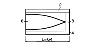
Figure 1 shows a side view of a device or decoupler according to the present
invention.
The decoupler has a layer of metal forming a first conducting side wall 2
spaced apart
from and parallel to a another layer of metal forming a second conducting side
wall 4.
These two side walls enclose a dielectric material 6 which may be air or may
be one or
more layers of material such as PET. The two conducting side walls define a
sub
wavelength cavity, one end of which is closed by a conducting end or base
portion 8.
One or both of the first and second conducting side walls 2, 4 may be
continuous with
the conducting base portion 8. The end of the cavity opposite the conducting
base
portion 8 is an open end, i.e. it has no conducting wall. The conducting base
portion 8 is
the only conducting link between the first and second side wails 2, 4. The
decoupler is
shown in Figure 2 in perspective view. For clarity no solid dielectric layer
is shown.
The device is designed to decouple radiation at a particular frequency. It is
convenient to
consider a simplistic model of the functionality of the decoupler, in which RF
waves are
coupled into the cavity and propagate along inside it until they reach either
a closed end
e.g. metal wall, or an open end. A proportion of the wave is reflected at the
end (whether
the end is open or closed) and travels back along inside the cavity.
CA 02655451 2008-12-15
WO 2007/144574 PCT/GB2007/002105
19
When the length of the cavity is just right the waves running back and forth
set-up
standing waves. The standing waves lead to the creation of regions of very
high electric
field - the electric field is resonantly enhanced. An RF tag which operates at
that
frequency which is located near to/in the high-field region is forced into
operation.
The electric field will be a minimum next to the metai wall or base portion
(closed end)
and a maximum at the open end. Therefore the standing wave pattern formed is a
quarter wave pattern, as illustrated in figure 1. Therefore where L = Ad/4,
where Ad is
equal to the wavelength of incident radiation within the dielectric material
(which is equal
to the free space wavelength divided by the refractive index of the dielectric
material,
Ao/n), a quarter wave standing wave pattern will be generated within the
dielectric
material of the cavity. This leads to a very high field at the frequency of
interest within
the vicinity of the open end, whatever material the decoupler may be mounted
on.
Therefore a tag can be placed on or near the open end to couple to the
enhanced field in
this region.
Figure 3 shows some possible positions where a tag could be located on a
decoupler.
An RF tag 10 could be located on the first conducting side wall 2 across the
end of the
side wall. The tag is located on a spacer (not shown) to separate it slightly
from the
surface of the conducting material. The electric field in this region is high
and would
couple well to the tag antenna. Alternatively a tag 12 could be located within
the cavity,
close to the open end. The figure shows the tag 12 only schematically, and it
will be
appreciated that the precise orientation of the tag within the cavity will
depend on the
precise geometry of the tag and cavity. Given the low thickness of many
embodiments, a
planar tag will most likely be located in the cavity, substantially parallel
with the upper
and lower layers.
Figure 4 shows a plan view of a commercially available standard UHF tag (for
example
an 866MHz Alien Technologies UHF 'Squiggle' Tag), comprising a chip 20 having
an
integral antenna 22. The width, w, of the tag is 8mm and the length, I, of the
tag is
95mm. It can clearly be seen that the majority of the size of the tag is due
to the antenna
(a typical situation for a commercially available UHF RFID tag). The chip
itself is much
smaller, in the order of 1-2mm. The antenna is tuned for free space operation
although
different antennas could be used which are tuned for a tag used in a
particular
environment. Operation in a different environment would require a different
tuned
antenna. The present invention allows such a tag tuned for free space to be
mounted on
CA 02655451 2008-12-15
WO 2007/144574 PCT/GB2007/002105
a decoupler and then used satisfactorily in a large number of environments
where
performance would normally be degraded.
Some RF tags possess directional antennas (i.e. antennas that preferentially
interact
5 with linear polarisation of a specific orientation) and therefore may only
operate correctly
when the tag is correctly orientated with respect to the reader to ensure that
radiation
incident at the tag and/or emitted by the tag matches the polarisation of
radiation emitted
or received by the reader. When the tag is mounted on the surface of the
decoupler it
should therefore be generally arranged in line with the axis of the cavity.
The need for correct orientation is not necessarily an issue for certain
applications, for
instance on standard packaging where the tag and decoupler are located in a
known
place and orientation on the article. Orientation issues may also be overcome
by using
transmitter/receiver systems which utilise circular or elliptical
polarisations, or multiple
and differently-aligned antennas. For instance Figure 5 shows two quarter wave
decouplers of the present invention, one on top of the other and rotated by 90
.
Radiation of the appropriate wavelength having a first polarisation would
create a
standing wave in one of the decouplers. Radiation of the orthogonal
polarisation would
create a standing wave in the other decoupler. Were each decoupler to carry an
appropriately located RF tag then one would be activated whatever the
polarisation of
the incident radiation. Obviously the two decouplers could be in the same
plane instead
of located one on top of another and two or more separate decouplers could be
used in
different orientations. Figure 6 shows an alternative arrangement where the
decouplers
are in the same plane, but the side walls are not in the same plane. Such an
arrangement could find application at the corners of objects for example.
Two decouplers could be located back to back. Figure 7 shows a side view of a
two
decouplers in a back to back arrangement. The two decouplers share a common
conducting end portion 8. The top side wall of the left hand decoupler 2 can
be a
continuous layer with the top side wall 14 of the right hand decoupler or they
may be
separate. Similarly the lower side wall 4 of the left hand decoupler may be a
continuous
layer forming lower side wall 16 of the right hand decoupler also.
The length of the cavity on the left is L, and the length of the cavity on the
right is L2.
Whilst these cavities could be the same length it may be advantageous to
ensure that
they are different lengths, each cavity being arranged to couple radiation at
a different
CA 02655451 2008-12-15
WO 2007/144574 PCT/GB2007/002105
21
wavelength. Thus a tag 10 or 12, which operates at a frequency corresponding
to a
wavelength of 4L, could be located on the left hand decoupler and a different
tag, 18,
which operates at a frequency corresponding to a wavelength of 4L2 could be
located on
the right hand decoupler. This would allow two different tags to be mounted on
a device
and both to work. This could be useful in tagging items travelling around the
world where
different frequencies are used. Even if only one tag is to be used this design
of
decoupler allows a user a choice of tag frequency. Figure 8 shows a similar
back to
back decoupler design from a perspective view point.
Another design of decoupler which allows different wavelengths to be decoupled
is
shown in figure 9. Here two decouplers are in effect stacked on top of each
other and
share a common second conducting side wall. A first cavity of length AB/4 is
formed by
conducting layer 30, dielectric 32 and second conducting layer 33. The cavity
is closed
at one end by conducting base portion 37. Note that the dielectric material 32
and
second conducting layer 33 both extend beyond the first conducting layer 30.
The length
of the cavity is determined by the length of area of overlap, i.e. the length
of the first
conducting layer 30. A second conducting cavity is formed by a third
conducting layer
35, dielectric 34 and second conducting layer 33 with one end being closed by
conducting base portion 37. Again the dielectric material 34 and second
conducting
layer 33 extend beyond the third conducting layer 35 and the length of the
cavity, defined
by the length of the third conductor layer, is AA/4. It will be clear
therefore that each
cavity will operate most effectively at a different wavelength and therefore
appropriate
tags 36 could be positioned in areas, which in use at the appropriate
frequency,
correspond to areas of high field.
Such an arrangement could be beneficial with decoupler cavities of the same
length. In
the arrangement shown in Figure 10 a tag placed with its antenna across the
open ends
of both cavities may benefit from the enhancing effects of the two cavities.
In essence,
two oscillating, in-phase dipoles are exhibited across AB and CD. A third is
created
across the metallic region BC, but this is out of phase with the other two. It
is believed
that, since BC is a much shorter distance than AB or CD, the field across BC
may
dominate, creating a higher field intensity than can be obtained via a single
cavity.
Alternatively, it may be possible to create a geometry in which the AB & CD
fields
dominate, driving currents through the antenna more efficiently than in the
case of a
single cavity. Although two cavities have been shown, the concept could be
extended to
three or more cavities joined in a similar fashion.
CA 02655451 2008-12-15
WO 2007/144574 PCT/GB2007/002105
22
Figure 11 shows an alternative embodiment in which two cavities have their
open ends
adjacent. A first cavity is formed by conducting layers 40 and 42. These
layers enclose
dielectric material 50. The cavity is closed at one end by conducting base
portion 46.
Conducting layer 42 extends to also form the side wall of a second cavity,
which further
comprises conducting layer 44. Conducting layers 44 and 42 also enclose
dielectric
material 50 and there is a conducting base portion 48 closing one end. A small
gap, or
aperture 52 between conducting layers 40 and 44 is located mid way between the
two
conducting base portions 46 and 48. The aperture provides an effective open
end for the
two cavities (aithough one could think of it as a half wavelength cavity which
is closed at
both ends and has a quarter wavelength slit therein). An RF tag located over
the
aperture 52 or within the dielectric material in the vicinity of the aperture
would be
located, in use, in an area of high electric field and would be decoupled from
any surface
effects.
Figure 12 shows a similar embodiment but having a spacer 54 between the two
cavities.
Figure 13 shows a different embodiment of a multiple cavity decoupler where
the cavities
are side by side and separated by a spacer 56 which may or may not be
conducting.
This could in effect by formed by a single quarter wave decoupler having an
aperture in
the top layer.
As mentioned the length of the decoupler cavity, and hence the wavelength at
which it
will optimally decouple, is determined by the length of area of overlap of the
two
conducting side walls. Generally the decoupler will be designed with a
particular
frequency in mind and so the length of the decoupler cavity will be constant
across its
width. This is conveniently achieved by ensuring the edge of the first
conducting side
wall which contacts the conducting base portion is substantially parallel to
the other
edge. However there can be advantages in deliberately changing the length of
the cavity
across the width. Figure 14 shows a plan view of the first conducting side
wall of a
decoupler according to another aspect of the invention.
The decoupler, generally indicated 60, has a first conducting side wall 62. At
one end 66
this connects to a conducting base portion to form a closed end. The other end
of the
decoupler is not parallel to the closed end 66 and instead the length of first
conductor
layer varies across the layer. This decoupler will therefore form standing
waves over a
CA 02655451 2008-12-15
WO 2007/144574 PCT/GB2007/002105
23
range of different frequencies and could again therefore be used with a range
of different
tags. The edges of the decoupler layers do not have to be linear and curved
edges
could be used.
It has been observed that a de-coupler, originally designed for 866MHz, can
also de-
couple tags that operate at 915MHz in free-space. By way of an example, the
Alien
Technologies 915MHz `Squiggle' tag is very similar to the Alien 866MHz tag -
the only
difference is in the main bulk of the antenna which is tuned for 915 MHz. The
antennas
for both tags incorporate an impedance loop and the relevant impedance loops
are
largely identical. It has been shown that the decoupler renders the main bulk
of the
antenna redundant. Hence when the antenna is on the de-coupler it is only the
impedance loop that matters.
The de-coupler is still intercepting power optimally at 866MHz and
intercepting virtually
no power at 915MHz as its performance curve is close to 0dB at this frequency.
Therefore the tag, despite being designed to operate at 915MHz, is being
driven into
operation at 866MHz. This is possible because the chip will operate almost as
well at
866MHz as it will at 915MHz. Therefore the decoupler intercepts power over a
frequency range, but the maximum performance wili be achieved when the
decoupler,
the reader and - to a lesser degree of importance - the tag all operate at the
same
frequency.
The present inventors have therefore realised that an RF tag could be used
which only
has a small antenna. As the decoupler couples radiation into its dielectric
core and
produces a high electric field at the open end of the cavity, a tag located in
this region will
be operating in an area of high field and will not require a large tuned
antenna. Thus the
decoupler of the present invention can be used with a so called low Q tag.
Figure 15
shows an example of a low Q tag, which has a small loop 70 which connects to a
chip
20. For example, the loop may be approximately 20mm in length. Referring back
to
figure 4 it can be seen that the tuned tag has a chip and effective inductance
loop but
also has a significant additional amount of tuned antenna structure. The low Q
tag can
therefore be thought of as a smaller variant of a tuned tag. The low Q tag
will not
function in free space unless the interrogating wavelength corresponds to the
antenna's
perimeter (e.g. 6GHz operation for a 5cm loop), and hence will not operate at
standard
UHF frequencies (e.g. 866 MHz) unless the reader is located within 1 or 2 mm
of the
chip, because the antenna 70 is inefficient at coupling to incident UHF
radiation. The low
CA 02655451 2008-12-15
WO 2007/144574 PCT/GB2007/002105
24
Q tag, which may be only slightly larger than the chip itself, may be placed
on any
decoupler according to the invention. Note that the small loop section may be
replaced
by short `arms' that extend outwards or partially wrap around a spacer, since
even two
short 'stubs' of metal are sufficient to couple power into the chip if
combined with a
correctly designed decoupler. Reduction in the antenna size allows for a more
compact
RF ID system without the need to wrap existing antennas around the body of the
decoupler. A yet further advantage is reduced materials for the RF ID
manufacture
process.
It has been found that the geometry of the decoupler, the materials from which
it is made
and the position and orientation of the tag with respect to the decoupler
influence the
performance of the system, which in turn determines the range at which the tag
can be
read. A series of experiments for creating optimised decoupler designs are now
described with reference to Figures 16 to 29. Maximum read-range is the most
common
parameter by which the effectiveness of the design changes is measured.
To a first approximation the wavelength in the decoupler core (Aco,.e ) is
related to the
wavelength in free-space (AFree-space ) by the refractive index n, as
_ a Free-space
A core "
yz
The higher the refractive index of the material the more slowly the waves
travel through
it. The frequency of the waves remains constant resulting in their wavelength
being
reduced. Taking PETG (refractive index c.1.8) as an example, the requisite
length for a
quarter-wavelength decoupter is 48mm. This can be proved empirically by
starting with a
quarter-wavelength decoupler that is significantly longer than this and
recording the read-
range achieved as the decoupler length is reduced. Read-range using an Alien
AL870
866MHz reader system and the loop from an Alien World Tag as a function of
cavity
length is shown in Figure 16.
The reduction in length reduces the wavelength of radiation that is trapped
within the
core and increases the operating frequency of the decoupler. When the length
of the
decoupler is such that its operating frequency matches that of the reader
system the
CA 02655451 2008-12-15
WO 2007/144574 PCT/GB2007/002105
amount of power coupled into the decoupler is maximised and the read-range of
the
system is maximised.
When the length is reduced still further the operating frequency of the
decoupler
5 becomes greater than that of the reader system and the amount of power
coupled into
the decoupler decreases again resulting in the read-range falling.
It is apparent that the optimum cavity length lies between 48.5mm and 49mm
which is
close to the theoretical value of 48mm. The minor discrepancy is considered
due the
10 perturbation of the decoupler resonance by the tag: there with be an
additional reactance
due to the interaction of the metal components of the tag and the decoupler
which shifts
the resonant frequency of the system as a whole.
The thickness of a PET spacer between the tag (and loop) and the upper surface
of the
15 decoupler was varied from 50 microns to 3000 microns. An 866MHz reader
system was
used and the central loop of an 915MHz Alien Squiggle was used. The read-range
as a
function of spacer thickness is shown in Figure 17. The optimum spacer
thickness can
be seen to lie between 500microns and 1000microns.
20 The trend is as expected: as the spacer thickness is reduced the capacitive
coupling
between the top metal layer of the decoupler and the part of the loop that
overlaps it
increases. In the limit where the spacer thickness tends to zero, that side of
the loop
would be in contact with the upper metal layer. In this case the loop acts as
a short
between one side of the chip to which it is connected and the top metal layer.
This
25 eliminates the voltage across the chip thus no current flows and the system
ceases to
operate.
As the spacer thickness is increased beyond 1000microns the strength of the
electric
field is beginning to fall rapidly: the potential across the antennas
terminals is smaller and
the read-range is consequently less.
As stated above the decoupler functions by creating regions of greatly
enhanced electric
field which force a tag placed in any of those regions into operation. There
are several
locations on the decoupler where the electric field is high and others where
is it low-
valued. By changing the position of the tag on the decoupler from locations
where the
CA 02655451 2008-12-15
WO 2007/144574 PCT/GB2007/002105
26
electric field is high to locations where it is low it can be demonstrated
that it is the
electric field rather than the magnetic field that is being exploited.
Consider the quarter-wave decoupler as shown in Figure 18a. The electric field
is
strongest at the open end of the core or cavity (towards the right as viewed)
and goes to
zero at the closed end adjacent to the base portion joining the upper and
lower
conductors. The region of enhanced electric field extends beyond the edge of
the cavity
but its strength falls off exponentially as distance from the surface of the
decoupler
increases. The magnetic field is shown, for reference, in Figure 18b, and can
be seen to
be greatest close to the metal base portion and tends to zero at the open end
of the
cavity.
The electric field scale runs from OV/m to 50V/m. The incident wave has an
electric field
amplitude of 1V/m therefore the electric field has been enhanced by a factor
of
approximately 50. The magnetic field [free space value 1/377 A/m] scale runs
from 0 A/m
to 0.25A/m therefore the magnetic field has been enhanced by a factor in
excess of 70.
Various placement positions of a tag on a dielectric cavity are shown in
Figure 19, in
which the incident electric field is in the direction shown by arrow 1910,
substantially
perpendicular to the base portion 1900. A tag can be placed anywhere along
Side 1,
which is opposite the base portion 1900, as shown at 1902, and can be read
typically at
a range of 4m for a 50mm wide PETG core decoupler. It is noted that the tag
can also be
folded around the open edge of the core as shown at 1904. The tag can also be
positioned along Side 2 as shown at 1906 for example. The electric field
strength
increases moving along side two away from the metal base portion. As expected
this
causes an increase in the read-range, as illustrated in the graph of Figure
20.
In this case the decoupler core was 4mm thick with a cavity length of 67mm
The maximum read-range occurs some 20mm in from the edge of the cavity along
Side
2.
Moving along the cavity from the base portion towards the open end the
electric field and
therefore the voltage is increasing and the magnetic field and the current are
decreasing
- the impedance is therefore increasing. It is suggested, although the
applicant is not
limited by this suggestion, that the read-range is a maximum at a short
distance away
from the edge because of slight impedance effects.
CA 02655451 2008-12-15
WO 2007/144574 PCT/GB2007/002105
27
Considering the electric field strength along the open end (Side 1 of Figure
19) this
remains high along the entire length of the open end, hence tags placed
anywhere along
that end can be read. However, there has been found to be some minor variation
in the
maximum read-range that can be achieved when the tag is moved along this edge,
as
illustrated in Figure 21.
The maximum read-range is achieved near to the centre of the edge and the
minimum
read-range occurs at the edges. The tag itself is asymmetric and this is
believed to be
the source of the slight asymmetry in the results.
If the electric field is parallel to a line drawn directly from one antenna
terminal to the
other, as shown in Figure 22b, then the voltage between the two terminals will
be a
maximum, and the read range will be correspondingly high. If the field is
perpendicular to
the line, as shown in Figure 22a, then the two terminals will be at the same
potential:
there will be no current flow between them and the tag cannot be read (this
assumes a
locally uniform electric field). At angles between perpendicular and parallel
the decoupler
should function but at a reduced range. An experiment was conducted to
determine the
relationship between read range and angle. The read-range achieved against the
angle
of rotation is plotted in Figure 23.
It can be seen that when the field is parallel to the line between the
terminals of the
antenna (90 ) the read-range is 5m, when perpendicular to the field (0 ) the
read-range
is zero.
The variation in performance of the device with offset of a chip and loop from
the edge of
the upper conducting plane will be described with reference to Figures 24 to
27.
The position of the coupling element, or loop, relative to the edge of the
upper
conducting layer was varied from -1 mm to +11 mm as shown in Figure 24. The
distance
between the reader antennas and the tag was kept constant whilst the power
output of
the reader system was progressively reduced from the maximum (2Watts) until a
threshold value was reached below which the tag could not be read: the lower
this
threshold value the better the tag is performing.
CA 02655451 2008-12-15
WO 2007/144574 PCT/GB2007/002105
28
Plotting the threshold power versus coupling element position results in a
graph that has
its lowest value where the tag is performing best. To make the graph more
intuitive it has
been reversed by subtracting from 2Watts (the maximum output power of the
reader
system) the threshold power value. This results in a graph of "surplus power"
which has
its greatest value where the tag is performing best.
Theoretical modelling allows the voltage across the chip to be calculated as
the coupling
element is moved relative to the edge of the upper conductor. A series of
models were
created in which the coupling element was moved from -8mm to +14mm and the
peak
voltage across the chip in each configuration was calculated. In this case the
power
incident on the tag remained constant therefore a larger voltage indicates a
better
performing tag. The voltage values were scaled such that the modelled peak
voitage
value had the same magnitude as the peak surplus power value measured by
experiment to make comparison between the two data sets easier. These results
are
plotted in Figure 25.
The voltage across the chip increases at it is moved away from 0mm off-set
where the
chip is directly above the edge of the upper conducting layer and reaches a
maximum at
+10mm beyond which it decreases rapidly. This behaviour can be explained by
examining the strength of the electric field around the decoupler.
A plot of the magnitude of the electric field on a plane perpendicular to the
decoupler is
shown in Figure 26. The plot clearly shows that the region of enhanced
electric field
extends only a short distance beyond the open end of the decoupler cavity
c.15mm from
-5nim to +10mm from the edge of the upper conductor.
For clarity the conducting layers have been show as a dotted line. Note that
the scale in
Figure 26 runs from 20V/m (black) to 110V/m (white) and that the incident
electric field
strength (wave ampiitude) was 1V/m. This demonstrates that there is electric
field
enhancement by a factor of 110 at the open edge of the cavity.
The loop used in this example is 22mm long and therefore extends approximately
10.5mm to each side of the chip (the chip is c.1mm square). Beyond +10.5mm the
loop
no longer overlaps the edge of the upper metal iayer where the field is
highest therefore
further displacement of the loop away from the edge of the upper conducting
plane
CA 02655451 2008-12-15
WO 2007/144574 PCT/GB2007/002105
29
exposes the loop to a progressively weaker field therefore the voltage across
the chip
and the surplus power both decrease.
With the chip directly above the edge of the upper conductor (0mm off-set) the
voltage
has a local minimum and the tag cannot be read. The failure to read may be due
to the
voltage being too low to active the chip.
The theoretical model predicts that the voltage should rise again as the
coupling element
is moved further over the upper conducting layer - has a negative off-set. The
voitage
falls away rapidly between -2mm and -4mm which is due to the asymmetric
distribution
of the enhanced electric field about the edge of the tuning plane as can be
seen from
Figure 3. The experimental measurements were not extended beyond -1mm so this
prediction cannot be verified.
This behaviour demonstrates that the decoupler is acting as a device for
creating a
highly localised voltage which is then transferred to the chip via capacitive
coupling
between the decoupler and the loop: the voltage across the chip and the
surplus power
remain high whilst the portions of the loop adjacent to the chip are within
the enhanced
field region. Outside of this region the potential gradient (electric field
strength) is low
hence the voltage across the chip is low. This mechanism of operation is in
accordance
with the properties discussed with reference to Figure 22, in which the loop
is roatated
through 90 in the plane of the decoupler. This places the sections of loop to
either side
of the chip in regions of equal electrical potential resulting in a zero
voltage across the
chip. Experiments have confirmed that in this orientation the tag cannot be
read.
Considering now the thickness of the dielectric resonant cavity, an experiment
was
performed in which the thickness (denoted by t) of the decoupler core was
varied
between 0.125mm and 3mm. The optimum cavity length for each core thickness was
determined by progressively reducing the cavity length and recording the read-
range. In
all cases the core material was polyester and the metal layer was formed from
aluminium
foil. The results are plotted in Figure 27.
As expected for all the decouplers the read-range hits a peak when the length
of the
cavity is such that its resonant frequency matches that of the reader system.
The peak
read-range is much greater for thicker cores than for thinner cores. This
variation of
maximum read-rage with core thickness is more clearly shown in Figure 28.
However, it
CA 02655451 2008-12-15
WO 2007/144574 PCT/GB2007/002105
will be understood that there is a trade off between thicker cores and the
overall
thickness of the component. For any given application there will be a suitable
core
thickness which provides sufficient read range while maintaining a low profile
device.
5 Since the lower layer of the decoupler is metal and the objects onto which
the decoupler
is placed are often metal, embodiments of the invention use the metal of the
object to be
tagged as the lower conducting layer. In this case the decoupler becomes a 2-
layer
device: the upper conducting layer and the dielectric core.
10 The quarter-wavelength decoupler requires a continuous conducting path
around three
sides of the dielectric core, hence care must be taken when utilising an
object onto which
the decoupler is mounted as the lower layer, to avoid substantial
discontinuities. A series
of tests were performed to asses the various configurations as illustrated in
Figure 29,
and the resulting read-ranges.
In all cases the core material was polyester and the tests were carried using
the 915MHz
system. The decoupler was 50mm wide and when optimised found to have a maximum
read-range of 6.Om for a cavity length of 44mm. The decouplers were fixed to a
metal
plate larger in extent than the decoupler during the determination of the read-
range.
The foil used in making these decouplers is in fact coated with a thin,
insulating polymer
layer such that when two layers are arranged parallei together there is little
or no direct
current flow between them. Each configuration introduces different possible
sources of
discontinuity, as illustrated by the lines of the figures.
It was found that the discontinuities give rise to lower read-ranges with each
discontinuity
reducing the range by c.40% of the maximum value for a decoupler with a truly
continuous conducting layer. Therefore designs with two discontinuities tend
to have
lower read ranges than designs with one discontinuity which in turn perform
less well
than decouplers with no discontinuities. The only exception to this rule is
Configuration 2
where poor electrical contact between the foil and the metal back plate is the
likely cause
of the reduced read-range.
Figure 30 shows an embodiment of a quarter wave decoupler arranged as a
quadrant or
quarter circle. An advantage of this arrangement is that orientation
dependency is
reduced.
CA 02655451 2008-12-15
WO 2007/144574 PCT/GB2007/002105
31
A given decoupler and tag configuration performs optimally when the resonant
dimension
of the decoupler is parallel to the incident electric field vector. As the
decoupler is rotated
read-range falls reaching zero when the resonant dimension is perpendicular to
the
electric field.
In the example of Figure 30, the decoupler is made from aluminium foil and 4-
5mm thick
corrugated cardboard as the dielectric cavity. The decoupler forms a 90
sector with a
continuous piece of foil running over the upper face, around the curved edge
and across
the lower face. The two straight edges do not have conductors extending over
the edges.
A tag is arranged at the vertex of the straight edges as shown in Figure 30
The radius of the quarter circle was progressively reduced in order to
determine the
optimum value. Starting from a radius of 158mm the tag was progressively cut
down
from the arcuate edge and a maximum read-range of 5.5m found to occur at a
radius of
121 mm.
A further embodiment is similar to that of Figure 30 but with the corner at
which the two
straight sides meet truncated to produce a third straight side 27mm long at
450 to the
other two. The maximum read-range was found to be 8m which occurred for a
radius of
120mm.
The azimuthal dependence of a quarter circle decoupler was then investigated.
The
decoupler was rotated through 360 in a plane parallei to that of the reader
antenna and
containing the incident electric field vector. The results are summarised in
Figure 31 with
the electric field indicated by the block arrow, and the solid line on the
decoupler
representing the long axis of the tag.
The read-range remains constant at 6m for all angles between 0 and 90 and
between
180 and 270 . This is to be expected as within these angular ranges the
electric field
vector is always parallel to a line drawn radially from the corner closest to
the tag such
that it lies across a metallic region and therefore is continually sampling
the correct
resonant dimension. This enables efficient coupling to the resonant mode
within the
decoupler core. The ranges 90 -180 and 270 -360 returned a read-range of
zero as
the electric field vector is never parallel to the resonant dimension within
this range. Thus
CA 02655451 2008-12-15
WO 2007/144574 PCT/GB2007/002105
32
the quarter-circle decoupler exhibits orientation independence between 0 and
900 and
between 1800 and 270
Figure 32 shows a decoupler which again has an arcuate base portion connecting
the
upper and lower conducting planes, but this time is semicircular in shape. A
slit is cut in
the upper part of the conducting layer (as shown by slit 1 in Figure 32b),
extending
perpendicular from the centre of the straight edge, approximately half of the
radius of the
decoupler in length.
With the tag wrapped around the straight edge of the decoupler at its centre
(as shown in
Figure 32a, but with the slit obscured), at a range of 0.5m the tag could be
in read in all
orientations (360 rotation in a piane parallel to that of the reader antenna)
with the
exception of a 10 band about the orientation at which the straight edge of
the decoupler
was parallel to the electric field of the incident waves. As the distance
between the
decoupler and the reader antenna was increased the range of angles over which
the tag
could be read decreased - the orientation dependency increased.
With the tag placed on the top surface of the decoupler, perpendicular to and
with its
terminals across the slit (as per the. tag orientation of Fig 29b) it could be
read at several
metres when the straight edge of the decoupler was parallel to the electric
field but the
read range fell to zero if the decoupler was rotated more than 45 .
A second, shorter slit (approximately 10mm long) was cut at the end of and
perpendicular to the first slit thus forming a T-shaped aperture in the upper
part of the
conducting layer (as shown as slit 2 in Figure 32b). With the tag wrapped
around the
decoupler (over the longer slit as per Fig 32a tag configuration) it could be
rotated 360
and the tag remained readable with only a few 'dead spots' observable.
It will be understood that the present invention has been described above
purely by way
of example, and modification of detail can be made within the scope of the
invention.
Each feature disclosed in the description, and (where appropriate) the claims
and
drawings may be provided independently or in any appropriate combination.