Note: Descriptions are shown in the official language in which they were submitted.
CA 02655463 2008-12-15
WO 2007/147132 PCT/US2007/071367
-1-
CONTINUOUS GAIN COMPENSATION AND FAST BAND SELECTION IN A
MULTI-STANDARD, MULTI-FREQUENCY SYNTHESIZER
BACKGROUND
Field of Invention
The present invention is directed to a wideband, low power frequency
synthesizer
including gain compensation and operating frequency band selection and
calibration.
Discussion of Related Art
In a wireless transmitter, a typical application for a frequency synthesizer
is to provide
a local oscillator signal (LO) to a mixer which in turn is used to up-convert
a modulated data
signal to a higher, radio frequency (RF), signal that is suitable for
transmission over an antenna.
If, as for example with the Global System Mobile (GSM) standard, a constant-
envelope
modulation is used, then the output of the frequency synthesizer can be
directly modulated to
superimpose modulated data on the voltage controlled oscillator (VCO) output.
Referring to
FIG. 1, there is illustrated an example of a conventional frequency
synthesizer 100 including a
VCO 102 in a phase-locked loop. The phase locked loop includes a programmable
divider 110,
a phase detector 112 (which also receives a reference frequency on line 114),
a charge pump
116 and a loop filter 118. The output of the VCO 102 is fed back into the loop
via an amplifier
120, as shown in FIG. 1. One method and apparatus for directly modulating the
VCO 102 at
the output of the frequency synthesizer is to provide a path for data
modulation through a so-
called Sigma-Delta modulator 104. By summing properly formatted and clocked
data
(entering the sigma-delta modulator on line 106) with a constant frequency
control word going
into the modulator on line 108, the data signal can be superimposed on the
final frequency
synthesizer output.
A problem with this approach is that the data is shaped in the frequency
domain by the
low-pass frequency response dynamics of the phase-locked loop. If the
bandwidth of the data
signal is greater than the low-pass bandwidth of the loop, then the data
signal will be
undesirably shaped or distorted. To compensate for this distortion, the same
data signal that is
applied to the sigma-delta modulator on line 106 (data path 1) may also be
used to modulate
the voltage controlled oscillator by way of a second data path with a high-
pass filter response.
The superposition of data signals from both paths onto the output of the
frequency synthesizer
can then yield a flat response for data at the output port of the frequency
synthesizer. The
CA 02655463 2008-12-15
WO 2007/147132 PCT/US2007/071367
-2-
method and apparatus for using two data paths to modulate the frequency
synthesizer output is
referred to as Two-Point Modulation.
Referring to FIG. 1, data entering the frequency synthesizer on line 106,
i.e., through
data path one, is in digital format. Data entering the system, on line 122,
i.e., through data path
two, may also be in the form of a digital signal. Therefore, a digital-to-
analog converter 124
may be placed in series with data path two so that an analog signal is input
to the VCO 102. In
addition, an amplifier 126 with a variable gain G can also be placed in the
path, between the
digital-to-analog converter 124 and the VCO 102, as illustrated in FIG. 1. It
can be shown that
in order for the overall frequency response for data modulating the frequency
synthesizer
output to remain flat, (i.e. undistorted), the variable gain G must meet the
requirement:
G=Fref/Kv2. Here, the value of the reference frequency Fref (input to the
frequency
synthesizer on line 114) is determined by the system design and is therefore a
known quantity.
However, the value of the gain of the auxiliary port into the VCO, Kv2 (in
units of MHz/V), is
a quantity that can experience variations due to changes in circuit operating
conditions, for
example, fluctuations in temperature and supply voltage.
In general, conventional methods for compensating for variations in the gain
Kv2 in
Two-Point Modulators involve digital measurements and calibration with
periodic updates.
However, such methods may suffer from limitations imposed by the time that a
system is
allowed for a calibration update, since the process is disruptive to the
actual operation of the
frequency synthesizer and a phase lock must be reacquired after each
calibration step. One
example of a method of gain compensation is given in U.S. Patent No. 5,307,071
to Arnold et
al., entitled "Low noise frequency synthesizer using half integer dividers and
analog gain
compensation," which is herein incorporated by reference, Another example of a
method of
gain compensation is disclosed in U.S. Patent No. 6,700,447 to Nilsson
entitled "Trimming of
a two point phase modulator," which is also herein incorporated by reference.
These examples
rely on the introduction of extraneous calibration sequences, and therefore
suffer from the
major disadvantage that the calibration sequences can introduce noise, or
frequency spurs, into
the frequency synthesizer, thereby severely degrading system performance.
Besides gain compensation, frequency calibration can be another important
consideration. Conventional frequency calibration approaches have the
disadvantage in that
they take too long to settle to a final selection of the appropriate band,
particularly if the
number of bands approaches 32 or even 64 (corresponding to a 5 or 6 bit VCO
band control).
One example of a conventional frequency calibration method is a successive
approximation
CA 02655463 2008-12-15
WO 2007/147132 PCT/US2007/071367
-3-
method which uses a race counter, as illustrated in FIG. 2. In this example, a
VCO 102
employed in a phase locked loop configuration is locked to a particular
reference frequency,
Fref, by dividing it with a frequency divider 110 having a division ratio N,
and comparing the
result to Fref (see FIG. 1). As illustrated in FIG. 2, the same VCO 102 and
programmable
divider 110 can be used in an open loop manner to compare the results of a
counter 128 that
receives the divided VCO signal to the result of an identical counter 130 that
receives the
reference frequency signal on line 132. Each counter 128, 130 counts pulses of
the divided
VCO signal and the reference frequency Fref, respectively, and the results are
compared by
race logic circuitry 134. The methodology is such that the first counter to
complete its count is
used as an indicator of which frequency is higher, either the reference
frequency (Fref) or the
divided VCO frequency (Fvco/N). If the divided VCO frequency (Fvco/N) is
higher, it is an
indication that the VCO 102 needs to be set to a lower frequency band.
Accordingly, the VCO
band can be set to a new value, and the count comparison is repeated. This
procedure is
repeated using a successive approximation algorithm for searching through the
VCO bands to
find the appropriate band in which the desired VCO frequency (N*Fref) can be
found. Once
the appropriate band has been found, the VCO 102 can be set in order for the
phase-locked
loop to successfully acquire a lock with the reference frequency.
In a race counter system, the size of the counter is a function of the
required accuracy
required for the final band decision. In turn, the required accuracy is a
function of the amount
of overlap between the bands. As an example, if a frequency accuracy,
Faccuracy, of 500 kHz
is needed, then it can be shown that the counter value, M, is governed by the
equation:
Faccuracy=Fref/(M-1) (1)
Thus, for a 50 MHz reference frequency, a counter value of 105 is needed.
Counting 105
cycles of a 50MHz signal takes approximately 2.1 s. Carrying out this
procedure for each bit
of a six bit band selection scheme would therefore require 12.6 s.
SUMMARY OF INVENTION
Aspects and embodiments of the invention are directed to a frequency
synthesizer that
includes a method of gain compensation, a method of fast voltage controlled
oscillator (VCO)
band calibration, and that is capable of high speed, wideband operation. Such
a frequency
synthesizer may be used in many applications, and in one example, may be
particularly
suitable for use in a multi-band, multi-standard transmitter or radio
transceiver.
CA 02655463 2008-12-15
WO 2007/147132 PCT/US2007/071367
-4-
In one embodiment, there is provided a method for continuous gain compensation
in a
Two-Point Modulation frequency synthesizer that may involve no extra
calibration sequences
and may take advantage of the realization that all the information necessary
for continually
compensating the gain of the second data path may be already present in the
system. In
another embodiment, there may be provided a method for VCO band calibration
which can
reduce the locking time in half (compared to the 12.6 s discussed above) by
using
predetermined initial settings for which bands should be used for which
frequencies. In yet
another embodiment, there may be provided a frequency synthesizer including a
programmable
divider with a very wide range of programmable division ratios. The
programmable divider
may be capable of operating at very high frequencies and at low power by
interfacing directly
to the VCO. In one example, a source-coupled logic approach may be used for
the design of a
cascaded chain of divider blocks that may allow for the use of a low power
supply. These
features may facilitate design of a frequency synthesizer that may be flexible
(capable of
synthesizing local oscillator carrier frequencies for a wide range of
communication standards),
efficient and fast.
According to one embodiment, a method of voltage controlled oscillator band
calibration in a frequency synthesizer may comprise acts of setting a value of
a band selection
control signal to an initial setting based on an expected frequency band in
which an operating
center frequency is located, iteratively adjusting the value of the band
selection control signal
to search one frequency band setting above and one frequency band setting
below the initial
setting until a proper setting for an operating frequency band in which the
operating center
frequency is located is determined, and setting the value of the band
selection control signal to
the proper setting to tune a resonant frequency of the voltage controlled
oscillator into the
operating frequency band. The method may further comprise an act of fine
tuning the resonant
frequency of the voltage controlled oscillator to the operating center
frequency. In one
example, the act of setting the value of the band selection control signal may
include setting a
bit pattern for a digital control signal to control a plurality of switches to
activate selected ones
of a corresponding plurality of capacitors such that the resonant frequency of
the voltage
controlled oscillator is in the operating frequency band. In another example,
the act of fine
tuning may include adjusting a control voltage for a variable capacitor to
fine tune the resonant
frequency of the voltage controlled oscillator to the operating center
frequency. Furthermore,
the act of iteratively adjusting the value of the band selection control
signal may include
CA 02655463 2008-12-15
WO 2007/147132 PCT/US2007/071367
-5-
comparing a scaled version of the resonant frequency of the voltage controlled
oscillator to a
reference frequency using a race counter circuit.
Another embodiment is directed to a voltage controlled oscillator comprising a
plurality
of switchable tuning circuits that in combination provide a resonant circuit
that generates a
resonant frequency of the voltage controlled oscillator, and a controller
adapted to provide a
digital band control signal that controls switching in and out of the resonant
circuit the plurality
of switchable tuning circuits to select an initial resonant frequency band
setting. The controller
is further adapted to iteratively adjust a value of the digital band control
signal to search one
frequency band setting above and one frequency band setting below the initial
resonant
frequency band setting until a proper value of the digital band control signal
is determined to
select an operating frequency band for the resonant circuit that includes a
desired operating
center frequency of the voltage controlled oscillator. In one example, the
plurality of
switchable tuning circuits may comprise a plurality of switchable capacitors.
In another
example, the digital band control signal may include a plurality of bits and
the controller may
be adapted to set a bit pattern for the digital band control signal to control
a plurality of
switches to activate selected ones of the plurality of switchable capacitors
such that the
resonant frequency of the voltage controlled oscillator is in the operating
frequency band. The
voltage controlled oscillator may further comprising a fine tuning circuit
coupled to the
plurality of switchable tuning circuits and to the controller, and the
controller may be further
adapted to provide a fine tuning signal to the fine tuning circuit to fine
tune the resonant
frequency of the voltage controlled oscillator to the desired operating center
frequency. In
another example, the fine tuning circuit may include at least one variable
capacitor, and the
controller may be adapted to adjust a control voltage for the at least one
variable capacitor to
fine tune the resonant frequency of the voltage controlled oscillator to the
desired operating
center frequency.
According to another embodiment, a programmable two-point frequency
synthesizer
architecture may comprise a voltage controlled oscillator having a first port,
a second port and
an output, a programmable divider coupled to the output of the voltage
controlled oscillator
and adapted to receive a data signal, a phase detector having a first input
coupled to an output
of the programmable divider and a second input adapted to receive a reference
frequency, the
phase detector being adapted to produce a loop signal based on a combination
of the reference
frequency an a signal received from the programmable divider, a first loop
filter coupled
between an output of the phase detector and the first port of the voltage
controlled oscillator so
CA 02655463 2008-12-15
WO 2007/147132 PCT/US2007/071367
-6-
as to provide a phase locked loop including the voltage controlled oscillator,
the programmable
divider, the phase detector and the first loop filter, a variable gain
amplifier having an output
coupled to the second port of the voltage controlled oscillator, an input
adapted to receive the
data signal, and a control port, a correlation canceling circuit coupled to
the control port of the
variable gain amplifier and adapted to receive the data signal and the loop
signal. The
correlation canceling circuit may be adapted produce a control signal based on
the data signal
and the loop signal and to apply the control signal to the control port of the
variable gain
amplifier, and the control signal may be selected to continuously adjust a
gain of the variable
gain amplifier such that an output signal of the voltage controlled oscillator
divided by the
programmable divider is substantially equal to the reference frequency. In one
example, the
programmable two-point frequency synthesizer may further comprise a second
loop filter
coupled in parallel with the first loop filter between the output of the phase
detector and the
first port of the voltage controlled oscillator, a first switch coupled to the
first loop filter and
adapted to switch in and out the first loop filter, and a second switch
coupled to the second
loop filter and adapted to switch in an out the second loop filter, and the
programmable two-
point frequency synthesizer may be configured such that selective activation
of the first and
second switches causes one of the first and second loop filters to be active
in the phase-locked
loop.
One embodiment of a frequency synthesizer may comprise a voltage controlled
oscillator coupled in phase-locked loop configuration with a programmable
divider and a
charge pump, a first loop filter coupled between an output of the charge pump
and an input of
the voltage controlled oscillator, a second loop filter coupled in parallel
with the first loop filter
between the output of the charge pump and the input of the voltage controlled
oscillator, a first
switch coupled to the first loop filter and adapted to switch in and out the
first loop filter, and a
second switch coupled to the second loop filter and adapted to switch in an
out the second loop
filter. The frequency synthesizer may be configured such that selective
activation of the first
and second switches causes one of the first and second loop filters to be
active in the phase-
locked loop. In one example, the first and second switches may be MOS
switches. In another
example, a value of a control voltage applied to a gate of the first switch
may be selected so as
to open the first switch, thereby decoupling the first loop filter from the
phase locked loop. In
another example, the frequency synthesizer may further comprise at least one
additional loop
filter coupled in parallel with the first and second loop filters, and a
corresponding at least one
additional switch coupled to the at least one additional loop filter and
operable to connect and
CA 02655463 2008-12-15
WO 2007/147132 PCT/US2007/071367
-7-
disconnect the at least one additional loop filter from the phase-locked loop.
The first loop
filter may comprise a combination of resistors and capacitors selected and
configured to
implement a predetennined transfer function. Furthermore, in one example, the
programmable
divider may be directly coupled to an output of the voltage controlled
oscillator. The
programmable divider may comprise a plurality of cascaded fractional divider
blocks, wherein
a digital control signal is applied to each of the plurality of cascaded
fractional divider blocks
to activate selected ones of the plurality of cascaded fractional divider
blocks so as to set a
divide ratio for the programmable divider.
According to another embodiment, there is provided a method of controlling an
1o operating frequency of a frequency synthesizer. The method may comprise
acts of generating
a resonant frequency using a phase-locked loop that includes a first loop
filter and a second
loop filter, providing a selection signal that controls switching in an out of
the phase-locked
loop the first and second loop filters, and adjusting the selection signal to
control switching of
the first and second loop filters, based on the resonant frequency, such that
one of the first and
second loop filters is active in the phase-locked loop.
In another einbodiment, a programmable fractional-N divider may comprise a
plurality
of fractional divider blocks coupled together in series, each one of the
plurality of fractional
divider blocks having a control port adapted to receive a digital control
signal, wherein the
digital control signal activates and deactivates selected ones of the
plurality of fractional
divider blocks so as to set a divide ratio for the programmable fractional-N
divider. Each of
the plurality of divider blocks may comprise a plurality of flip-flops coupled
to digital
components. In one example, the digital components may comprise at least one
AND gate.
BRIEF DESCRIPTION OF THE DRAWINGS
Various embodiments and aspects of the invention are described in detail below
with
reference to the accompanying figures. It is to be appreciated that the
accompanying drawings
are not intended to be drawn to scale. In the drawings, each identical or
nearly identical
component that is illustrated in various figures is represented by a like
numeral. For purposes
of clarity, not every component may be labeled in every drawing. In the
drawings:
FIG. 1 is a block diagram of a frequency synthesizer einploying Two-Point
Modulation;
FIG. 2 is a block diagram of a conventional race-counter band calibration
circuit;
CA 02655463 2008-12-15
WO 2007/147132 PCT/US2007/071367
-8-
FIG. 3 is a block diagram of one example of a frequency synthesizer including
Two-
Point Modulation, according to an embodiment of the invention;
FIG. 4 is a diagram illustration one example of a voltage controlled
oscillator
implementation, according to an embodiment of the invention;
FIG. 5 is a graph illustrating an example of voltage controlled oscillator
tuning bands;
FIG. 6 is a graph illustrating a shift in the VCO bands of FIG. 5 due to
varying
operating conditions;
FIG. 7 is a block diagram of a modified race-counter circuit according to an
embodiment of the invention;
FIG. 8 is a block diagram of one example of a programmable divider
architecture
including a series of cascaded dividers, according to another embodiment of
the invention;
FIG. 9 is a logic circuit diagram of one example of a digital logic
implementation of
one of the dividers of FIG. 8, according to another embodiment of the
invention;
FIG. 10 is a circuit diagram of one example of a circuit implementation for
the logic
circuit shown in FIG. 9; and
FIG. 11 is a circuit diagram of one example of a frequency synthesizer
including
multiple switchable loop filter, according to another embodiment of the
invention.
DETAILED DESCRIPTION
According to aspects and embodiments of the invention, there is provided a
frequency
synthesizer capable of wideband operation and that may include a method of
gain
compensation that may not require external calibration sequences, as well as a
method of fast
VCO band selection. To facilitate wideband operation, embodiments of the
frequency
synthesizer may include switchable independent loop filters that may allow the
frequency
synthesizer to accommodate significant changes in bandwidth. In addition,
there are disclosed
methods of gain compensation and VCO band selection, as well as a fast,
wideband
programmable divider configuration that may be used in embodiments of
frequency
synthesizers according to the invention.
It is to be appreciated that this invention is not limited in its application
to the details of
construction and the arrangement of components set forth in the following
description or
illustrated in the drawings. The invention is capable of other embodiments and
of being
practiced or of being carried out in various ways, and the invention is not
limited to the
examples presented unless specifically recited in the claims. In addition, it
is to be appreciated
CA 02655463 2008-12-15
WO 2007/147132 PCT/US2007/071367
-9-
that the phraseology and terminology used herein is for the purpose of
description and should
not be regarded as limiting. The use of the words "including," "comprising,"
"having,"
"containing," or "involving," and variations thereof herein, is meant to
encompass the items
listed thereafter and equivalents thereof as well as additional items.
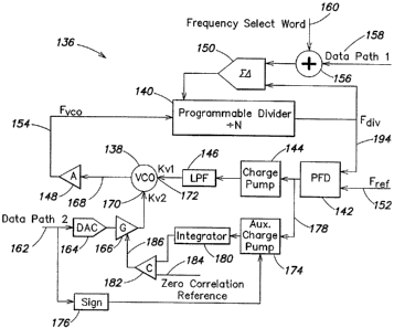
Referring to FIG. 3, there is illustrated a block diagram of one embodiment of
frequency synthesizer employing Two-Point Modulation and continuous gain
correction
circuitry, according to one embodiment of the invention. The frequency
synthesizer 136
includes a voltage controlled oscillator (VCO) 138 in phase-locked loop
configuration. The
loop includes a programmable fractional-N divider 140, a phase detector 142, a
charge pump
144 and a loop filter 146. In addition, the output of the VCO 138 may be
amplified by an
amplifier 148 before being fed back to the programmable divider 140. A
reference frequency
is fed to the phase-locked loop on line 152.
In one embodiment, the frequency synthesizer may further include a sigma-delta
modulator 150 for modulating a data signal (containing data to be transmitted)
onto a carrier
frequency generated by the frequency synthesizer. A carrier signal produced by
the frequency
synthesizer, herein referred to as Fvco on line 154, may be directly modulated
by providing a
path for data modulation through the Sigma-Delta modulator 150. By summing
(either in a
summer 156 or in the sigma-delta modulator itself) properly formatted and
clocked data on line
158 (referred to as data path one) with a constant frequency control word
provided on line 160,
the data signal can be superimposed on the carrier signal at the frequency
synthesizer output.
This may have the benefit of being a relatively simple method of modulation,
which may
reduce the overall complexity (by reducing the number of component blocks) of,
for example,
a transmitter in which the frequency synthesizer may be used. Fewer components
may reduce
the overall power consumption of the device, which may also be desirable. The
frequency
control word may be supplied, for example, by a microcontroller (not shown)
that may be
coupled to the frequency synthesizer.
According to one embodiment, the frequency synthesizer may use Two-Point
Modulation, in which the same data signal is also fed to the VCO 138 via a
second data path
(data path two). The digital data signal on line 162 may pass through a
digital-to-analog
converter 164 to be converted to an analog signal that may be fed, via a
variable gain amplifier
166, to the VCO 138. As discussed above, by using two data paths, one with a
low pass filter
response (i.e., the path that passes through the loop filter 146 of the phase
locked loop) and a
second path with a high pass filter response (data path two), the
superposition of the signals
CA 02655463 2008-12-15
WO 2007/147132 PCT/US2007/071367
-10-
from both data paths onto the carrier signal generated by the frequency
synthesizer can yield a
flat wideband response for the modulated data on the carrier signal at the
frequency synthesizer
output. In order for the overall frequency response of the data modulating the
carrier
frequency to remain flat, (i.e. undistorted), the variable gain G of the
variable gain amplifier
should meet the requirement: G=Fref/Kv2, where Kv2 is the value of the gain
(in units of
MHz/V) of the auxiliary VCO port 170 in data path two. Kv2 is a quantity that
may
experience variations due to changes in circuit operating conditions, for
example, fluctuations
in temperature and supply voltage. It may therefore be desirable that the
value of G
continuously tracks Kv2 to account for any such variations.
According to one embodiment of the invention, there is provided a frequency
synthesizer that may involve no extra calibration sequences and takes
advantage of the
realization that all the information necessary for continually adjusting the
gain of data path two
may be already present in the system. Under ideal system conditions, where the
gain G is
perfectly calibrated, introducing a data signal into both data paths, as
discussed above, may
result in a signal at the primary VCO control port 172 having a gain setting
Kvl, which may be
perfectly flat. If, however, there is a mismatch between the setting of the
gain G, and the value
of Fref/Kv2, there will be some residual data signal observable on the main
control port 172 of
the VCO 138. If the gain G is too small, the residual signal on the main
control port 172 may
exhibit a directly proportional correlation with the input data.
Alternatively, if the gain G is
too large, then the residual signal on the main control port 172 may exhibit
an inversely
proportional correlation with the input data. Based on this information and
knowledge of the
input data, a feedback control system can be developed that monitors this
correlation and
corrects the gain of the data path until there is zero correlation (or nearly
zero correlation)
between the observed signal on the main control port and the input data.
Referring to again FIG. 3, one embodiment of a frequency synthesizer according
to
aspects of the invention may include correlation canceling circuitry coupled
to data path two.
In one example, an auxiliary charge pump 174 may be used to mirror the
response of the main
phase locked loop. The auxiliary charge pump 174 may provide information
regarding any
residual signal in the main loop due to gain mismatch without directly sensing
the main VCO
control port 172. The sign of the input data may be sensed (by sign-sensing
circuit 176) and
may be used to reverse the polarity of the response of the auxiliary charge
pump 174 to the
signal from the phase detector 142 on line 178 which represents the residual
data signal in the
main loop. The output of the auxiliary charge pump 174 may be integrated, as
represented in
CA 02655463 2008-12-15
WO 2007/147132 PCT/US2007/071367
-11-
FIG. 3 by integrator 180. The direction and rate of change in the integrated
signal may provide
information about the correlation of the input data with the residual signal
in the main loop. A
correlation signal produced by integrator 180 may be compared in an error
amplifier 182 with
a zero correlation reference voltage, input to the error amplifier on line
184. The output of the
error amplifier 182 may provide a correction voltage on line 186 to the
variable gain amplifier
166 to control the gain G of data path two. In this manner, the gain G may be
continually
adjusted so as to maintain a flat, undistorted output signal from the VCO 138.
As an alternative, according to another embodiment, the residual data signal
of the
main loop may be directly sensed at the main control port 172 of the VCO 138.
However, it
should be noted that direct sensing of the main VCO control port could
potentially be
disruptive if any switch transients occur while tracking the sign of the input
data. These
transients, which may develop through capacitive coupling or switch charge
injection, could be
integrated by the loop filter 146 and undesirably affect the performance of
the main loop.
Therefore, in at least some embodiments, the above-described method in which
no direct
sensing of the main control port 172 of the VCO 138 is required may be
preferable.
As discussed above, another embodiment of the invention may be directed to a
method
of VCO band selection/calibration that may allow the frequency synthesizer to
achieve faster
locking times by reducing the time taken to select and appropriate VCO
frequency band. In
particular, predetermined initial settings may be used to limit the number of
frequency ranges
over which a search algorithm may be performed to find the desired operating
frequency band,
as discussed below.
Referring to FIG. 4, there is illustrated one example of a schematic circuit
implementation for the VCO 138. According to one embodiment, the VCO circuit
may use
cross-coupled PMOS transistors Q1 and Q2 to generate a negative resistance,
and use NMOS,
source-follower tail transistors Q3 and Q4 to control bias currents. The
degree of control may
be accomplished by a current source 196. A power supply source voltage may be
supplied at
terminal V. The carrier signal produced by the frequency synthesizer may
generally have a
known, desired operating center frequency, referred to as Fc and output from
the VCO on line
168 (see FIG. 3). For example, referring again to FIG. 4, the VCO 138 may
comprise a
tunable capacitive element in parallel with an inductive element 198 to
provide a resonating
structure that generates the carrier frequency Fe. The resonant tuning circuit
may comprise
inductors 198 (e.g., including inductors Ll and L2) that may be augmented by a
capacitor bank
200 as well as additional tuning capacitors as discussed below. In one
example, the VCO
CA 02655463 2008-12-15
WO 2007/147132 PCT/US2007/071367
-12-
resonant circuit may use fixed inductors formed by transmission lines in
conjunction with fixed
and variable capacitive elements. This architecture may provide an efficient
implementation of
a wideband tuning circuit for the VCO that may allow a tuning range of more
than a gigahertz.
According to one embodiment, the inductors L1 and L2 may be implemented as
bondwires that may be used to couple various circuit components to a
semiconductor substrate.
Each bondwire may have associated with it a certain inductance that may be
dependent on the
length of the bondwire, the cross-sectional area of the bondwire, and the
spacing between
adjacent bondwires (which affects mutual inductive coupling between the
bondwires). At a
given operating frequency, the inductance associated with the bondwires may be
approximated
by a fixed inductance, which is the inductance represented by L1 and L2 in
FIG. 4. It is to be
appreciated that each of L1 and L2 may be include one or more bondwires, and
also that
inductors 198 may include additional inductive elements as well. The use of
bondwire
inductors in a VCO resonant circuit may have several advantages, including,
for example,
providing better phase noise, lower power consumption, and wider tuning range
than may
conventional on-chip spiral inductors. Improved phase noise may be due to the
higher quality
factor (Q) of the bondwires with respect to on-chip inductors, such as spiral
inductors, and
extended tuning range may be due to the lower parasitic capacitance associated
with bondwire
inductors. In addition, conventional spiral inductors are relatively large,
and using bondwires
instead of such spiral inductors may allow for a smaller circuit footprint.
However, it is to be
appreciated that the invention does not require the use of bondwires for
inductors 198, and
other transmission line inductors or conventional inductors may also be used.
Referring again to FIG. 4, the capacitive element may include, for example, a
bank of
switchable fixed value capacitors 200 such that, by selecting which of these
capacitors are
active, a "band" of resonant frequencies may be selected. In one embodiment,
the VCO 138
may be configured such that it has a plurality of operating frequency bands.
The bank of
capacitors 200 may include, for example, a plurality of MOS (metal oxide
semiconductor) or
MIM (metal-insulator-metal) capacitors that may be switched electronically by
control signals
applied to the switches 202a...202b, 202c. It is to be appreciated that any
type of capacitor
may be used; however, MOS and MIM capacitors are common to CMOS and other
semiconductor circuits and may therefore be preferred in some embodiments. To
address the
tradeoffs between better circuit performance and wider microelectronic process
variations, the
switchable bank of capacitors 206 may be used to increase the overall tuning
range of the
VCO, while reducing its tuning sensitivity to abate the effects of
electromagnetic (EM)
CA 02655463 2008-12-15
WO 2007/147132 PCT/US2007/071367
- 13 -
coupling and further improve phase noise. This may be done by dividing the
overall tuning
range into frequency bands. In one example, the capacitors 200 may have
relatively large
capacitance values (e.g., on the order of tens of picofarads each) and a
desired operating
frequency band may be selected by switching in and/or out appropriate ones of
the capacitors.
According to one embodiment, a six-bit switched metal on metal (MOM) capacitor
array may be used for band selection. In this example, the capacitor bank 200
may include six
pairs of capacitors Col and C02 to Cõ1 and Cõz, where (in this example) n= 6.
Of course it is to
be appreciated that the invention is not limited to a six-bit case, and other
values of n may be
used, for example, a four-bit or eight-bit design. In addition, each bit need
not correspond to a
pair of capacitors, but may instead control one or multiple capacitors. A
digital control word,
referred to herein s the VCO band-select control signal, may be issued (for
example, by a
microcontroller) to activate switches 202a...202b, and 202c. In one example,
this control word
may be a binary word that may include a bit to control each of the switches.
For example, in
the illustrated six-bit case, bit 0 may control switch 202a, bit 5 may control
switch 202b and bit
6 may control switch 202c. The other intervening bits may control additional
switches not
shown in FIG 4, but represented by dots 204.
Once a frequency band has been selected, the desired center frequency Fe may
be tuned
within this band, for example, by controlling a variable capacitance (e.g., a
varactor diode) that
also forms part of the capacitive element of the resonating structure.
Referring to FIG. 4, in
one example, fine tuning within the selected frequency band may be achieved by
controlling
capacitance values of variable capacitors 206a and 206b. In one example, two
accumulation
mode MOS varactors Ct1 and Ct2 may be used for fine-tuning the frequency by
applying a
variable analog voltage (Vcontrol) through terminal 208. These varactors may
be implemented,
for example, as NMOS inside N-well varactors, although other designs may also
be used.
Embodiments of a VCO that may be used in the invention are disclosed in co-
pending,
commonly-owned U.S. Patent Application No. 11/202,626, entitled "PROGRAMMABLE
RADIO TRANSCEIVER," filed August 11, 2005, and which is herein incorporated by
reference, and in co-pending, commonly-owned U.S. Patent Application entitled
"PROGRAMMABLE TRANSMITTER ARCHITECTURE FOR NON-CONSTANT AND
CONSTANT ENVELOPE MODULATION," filed on even date herewith, and herein
incorporated by reference.
One example of the effective relationship between the bands that may be
selected by
controlling the bank of fixed capacitors, a control voltage that tunes the
variable capacitance,
CA 02655463 2008-12-15
WO 2007/147132 PCT/US2007/071367
-14-
and the VCO output frequency is illustrated in FIG. 5. As shown in FIG. 5,
once a frequency
band 0-7 has been selected by activating an appropriate bit pattern to switch
in and out, ones of
the bank of switchable capacitors, the value of the center frequency Fc may be
tuned within
that band by varying the control voltage (Vcontrol) to tune the variable
capacitance. Thus, in
at least one embodiment, the switched capacitors 200 may serve as a means of
coarse tuning,
and the variable capacitors whose capacitance can be adjusted via a variable
control voltage
(e.g., varactor diodes), may be used for fine tuning. It is of course to be
appreciated that other
resonant circuits for the VCO may also achieve the same result, namely that
the VCO
frequency may be tuned over and within several operating frequency bands, and
the invention
is not limited to the particular example given herein.
Table 1 below illustrates some examples of frequency band selection for three
different
VCOs that can be realized with a six bit binary pattern 0 - 63. It is to be
appreciated that the
frequency band values given for each VCO are exemplary only and not intended
to be limiting.
The actual band values for a given implementation may depend on the values of
the capacitors
200, the inductance values provided by inductor 198, the reference frequency
value (see, for
example, FIG. 1) and other factors.
TABLE 1
Bit Pattern VCO 1 VCO 2 VCO 3
Frequency
Bit5 Bit4 Bit3 Bit2 Bitl BitO Band Min. Max. Min. Max. Min. Max.
Freq. Freq. Freq. Freq. Freq. Freq.
0 0 0 0 0 0 0 1848 1863 2280 2299 4267 4397
0 0 0 1 1 1 7 1792 1806 2211 2226 3716 3803
0 0 1 1 1 1 15 1734 1746 2139 2153 3286 3348
0 1 0 1 1 1 23 1680 1691 2074 2087 2976 3021
0 1 1 1 1 1 31 1632 1642 2015 2026 2741 2777
1 0 1 1 1 1 39 1588 1596 1960 1971 2553 2582
1 0 1 1 1 1 47 1547 1554 1910 1920 2400 2424
1 1 0 1 1 1 55 1508 1516 1863 1872 2271 2291
1 1 1 1 1 1 63 1473 1480 1820 1828 2161 2179
The desired operating center frequency Fc may fall in any one of the operating
frequency bands of the VCO 138. In the absence of supply voltage changes,
temperature
CA 02655463 2008-12-15
WO 2007/147132 PCT/US2007/071367
-15-
fluctuations, and manufacturing process and parameter variations, one may have
a priori
knowledge as to which frequency band it would be appropriate to set the VCO to
in order to
maintain the desired frequency Fc. However, the aforementioned changes in
operating
conditions may have the undesired effect of shifting the bands to higher or
lower frequencies,
as illustrated in FIG. 5. As shown in FIG. 6, due to some changes in operating
conditions, the
VCO bands have shifted higher in frequency. As an example, whereas before Fc
could be
found in band 7, now Fc no longer falls within band 7. This illustrates how a
manual setting of
the VCO may become problematic in the presence of varying operating
conditions.
Consequently, in one embodiment of the invention, an intelligent method of
automatic
selection, or calibration, of the VCO's center frequency band may be provided
so as to ensure
that the desired frequency, Fc, is found within the selected band.
As discussed above, there are prior art methods of VCO calibration, such as
the race-
counter method. However, these methods may suffer the disadvantage that they
take too long
to settle to a final selection of the appropriate band, particularly if the
number of bands starts
approaching values of 32 or 64 (as would be the case for 5- or 6-bit VCO band
control, which
may be common for a multi-band frequency synthesizer). Therefore, according to
aspects of
the invention, there may be provided a method of VCO band calibration that may
vastly reduce
the settling time by using predetermined initial settings for which bands
should be used for
which desired center frequencies.
In some applications it may be highly desirable that the speed at which the
VCO
frequency band is determined be very fast. This may require very fast
synthesizer locking
times. An example of such an application is the GSM cellular standard for
mobile handsets for
which locking times may need to be as fast as 100 s. Often, it may be very
difficult to meet
such a fast locking time even without any consideration of VCO band selection.
If a VCO
band needs to be selected before the routine of acquiring a frequency lock in
the phase-locked
loop can be begun, it may become even more difficult to obtain a lock quickly
enough to
comply with standards such as the GSM. Therefore, some embodiments of the
invention are
directed to a method that may reduce the amount of time needed for VCO band
selection,
thereby allowing maximum time for the frequency synthesizer to obtain a lock.
In particular,
methods according to embodiments of the invention may allow minimal overhead
time
between switching synthesizer frequencies from one desired operating frequency
to another.
CA 02655463 2008-12-15
WO 2007/147132 PCT/US2007/071367
-16-
According to one embodiment of the invention, there may be provided a method
for
VCO band calibration in which an intelligent initial band selection may be
used to set the VCO
band very close to the appropriate band of operation. A modified binary search
algorithm may
then be used to search bands above or below the initial setting in such a
manner that only a few
iterations of a count and compare cycle may need to be repeated. In at least
one embodiment,
these methods may reduce the lock time in half compared to the 12.6 s taken
by some prior
art designs, as discussed above.
Referring to FIG. 7, there is illustrated a block diagram of one embodiment of
a
modified race-counter band calibration circuit according to an embodiment of
the invention. In
the illustrated example, a so-called race logic circuit 188 may receive inputs
from two M
counters 190, 192. The first counter 190 may receive as its input the
frequency Fdiv from the
programmable divider 140 (in the synthesizer's phase locked loop) on line 194.
The reference
frequency may be applied to the second counter 192 on line 152. Depending on
the intended
polarity of the circuit, if a signal is received from the second counter 192
before the first
counter 190, then the race logic circuit 188 may change the band select bits
(applied to activate
the switches 202 in FIG. 4) to operate the VCO at a higher frequency.
Conversely, if a signal
is received from the first counter 190 before the second counter 192, then the
race logic circuit
188 may change the band select bits to operate the VCO at a lower frequency
setting. In this
manner, the appropriate band of operation desired for the VCO output (divided
by N) may
iteratively converge to the reference frequency.
As discussed above, in a conventional race-counter design, the comparison of
the
counters may be repeated for a number of times equivalent to the number of
band select bits.
The size, M, of the counters may be a function of the accuracy desired for the
final band
decision and the reference frequency (Fref) selected for the synthesizer. In
addition, the
desired accuracy may be a function of the amount of overlap between the
frequency bands of
the VCO. For example, a GSM synthesizer using a reference frequency of 52MHz
and a VCO
having 6 bands to select from, an accuracy (Faccuracy) of 500 kHz would be
needed. As
mentioned above, since, an example value of Fref = 50 MHz would require a
counter value of
105. Counting 105 cycles of a 50 MHz signal takes about 2.1 s, and to do this
for each bit of
a six bit band selection therefore takes 12.16 s. Generally, the calibration
time may then be
calculated from the equation:
Tcal=[(1 /Faccuracy)+(1/Fref)] *VCO_bands. (2)
CA 02655463 2008-12-15
WO 2007/147132 PCT/US2007/071367
- 17-
where Faccuracy=Fref/(M-1) and M is the size of the counters.
According to one embodiment, a method for VCO band calibration can reduce this
calibration time in half by using predetermined initial settings for which
bands should be used
for which frequencies. An intelligent initial selection setting may set the
VCO band initially
very close to an appropriate band of operation. Referring again to FIG. 7, the
frequency
synthesizer may include, or may be coupled to, a memory device (not shown)
that includes a
look-up table and supplies the estimated value for bits of the VCO-band select
control signal
on line 210. This estimate may be based on, for example, the a priori
knowledge of which
band the desired center frequency Fc should fall, absent variations in
operating conditions.
The estimate is used to set initial values for the bits of the VCO band-select
control signal.
Then, the race-counter circuitry may be used to adjust the VCO band-select
control signal to
the appropriate band in which Fc is in fact located (taking into account
varying operating
conditions, as discussed above in reference to FIG. 6). Specifically, in one
example, a search
algorithm can be used that searches the two adjacent bands above or below the
initial setting.
This may provide a far more confined search space. As shown in FIG. 7, the
output from the
race logic circuitry 188 may be supplied on line 211 to a summer 213 where it
may be
combined with the estimate signal supplied from the look-up table, and then
fed to the VCO
138 to select a frequency band for the VCO. In such a manner, only three
iterations of the
count-and-compare cycle may be performed, even though the VCO may have eight
bands (for
6-bit control). In this particular case the time required to find the
appropriate frequency band,
Tcal, may be given by:
Tcal=[(1 /Faccuracy)+(1 /Fref)] *3 (3)
where 3 is fewer than the number of VCO bands. As can be seen from the above
equation, this
method may significantly reduce the time taken to locate the appropriate
frequency band,
thereby allowing the frequency synthesizer to lock to a desired center
frequency more quickly.
In a frequency synthesizer designed to accommodate a number of different
communication standards across many different frequency bands, the VCO 138
desirably
should be capable of producing a large range of output frequencies. Likewise,
the fractional-N
divider 140 desirably should be capable of a large range of division ratios in
order to divide the
VCO frequency (Fvco) to match the reference frequency (Fref) for frequency
calibration. Also,
in some embodiments of a multi-standard system, the VCO 138 may be likely to
oscillate at
very high frequencies, and the programmable divider 140 may therefore need to
interface to
the VCO at these very high frequencies.
CA 02655463 2008-12-15
WO 2007/147132 PCT/US2007/071367
-18-
Some prior art solutions avoid the need to design a divider capable of
operating at the
same frequency as the VCO by placing a so-called prescaler, having a division
value M, in
front of the programmable divider to reduce the frequency at which the
programmable divider
needs to operate. One example of such a design is disclosed in a paper by
Ahmed, et al.
("CMOS VCO-prescaler cell-based design for RF PLL frequency synthesizers,"
2000 IEEE
Proceedings ISCAS, Geneva, Volume 2, May 2000, pp. 737 - 740), which is herein
incorporated by reference. A drawback of this solution is that quantization
noise that may be
produced by the sigma-delta modulator in the frequency synthesizer (see FIG.
1) may be
multiplied by the value of the prescaler, M in the process of performing
fractional-N division
of the VCO output signal. In addition, the minimum value for frequency
division in the
fractional-N divider, Nmin, now may be limited by the product of M*Nmin. It
often may be
likely that for a multi-standard wideband system architecture, the minimum
division ratio may
need to be lower than what can be achieved using this method. An example of a
conventional
architecture that attempt to address this problem of limited programmable
division ratios by
using a cascaded arrangement of dual modulus 2/3 dividers, is disclosed in
paper by C.S.
Vaucher et al. ("A Family of Low-Power Truly Modular Programmable Dividers in
Standard
0.35-um CMOS Technology," IEEE J. Solid-State Circuits, vol. 35, pp. 1039-
1045, July 2000),
which is herein incorporated by reference. However, this example, though
capable of some
moderately high speeds, is not optimal for low power operation at very high
speed due to the
use of many stacked MOS (metal oxide semiconductor) devices which require a
high power
supply voltage.
According to some embodiments of the invention, there is provided a
programmable
divider with a very wide range of programmable division ratios. In addition,
the
programmable divider may be capable of operating at very high frequencies and
at low power
by interfacing directly to the VCO. In one embodiment, this may be achieved
through the use
of an alternative source-coupled logic approach for the design of cascaded
divider blocks that
allows for the use of a low voltage power supply, for example, by using a
reduced number of
stacked MOS devices.
Referring to FIG. 8, there is illustrated one example of an implementation for
the
programmable fractional-N divider including a series of cascaded fractional
divider blocks 1
through n. Each fractional divider block 212 may have, for example, a divide
ratio of 2/3 and
may include an input 214 to receive the VCO output signal Fvco, for the first
divider in the
chain, and the divided signal from the preceding divider for all other
dividers 212 in the chain.
CA 02655463 2008-12-15
WO 2007/147132 PCT/US2007/071367
- 19-
The outputs 216 of each divider, (except the last one in the chain), are
coupled to the input of
the next divider in the chain such that the signal can be divided successively
by 2/3. The
output of the last divider block in the chain may provide the frequency Fdiv
on line 194 (see
FIG. 3). In one embodiment, a control signal that comprises a number of bits n
equal to the
number of dividers in the chain may be applied to the dividers to control a
divide ratio of the
overall fractional-N divider 140. As illustrated in FIG. 8, a bit of the
control signal may be
applied to a mode-enable input 218 of each divider 212. Based on the setting
of the binary
inputs bO, b 1, ...,bn, which may be supplied, for example, by a
microcontroller, the overall
divide ratio may be set.
Referring to FIG. 9, there is illustrated one example of a logic
implementation of each
divider block 212 in FIG. 8. In the illustrated example, the divider blocks
212 may be
implemented using four D-latch flip-flops (220), three AND gates (222), and an
OR gate (224)
as seen in FIG. 9. The signal p indicates a permanent logic I state. This
design may be
advantageous in that it may be very simple and allow great flexibility
(because of the
combination of divide ratios supplied by the binary bit pattern b0...bn) while
involving few
components and therefore allowing low power operation. In addition, in
contrast to the design
disclosed in the paper by Vaucher et. al, referenced above, this embodiment
does not require
the use of many stacked MOS devices, which are typically high-power devices.
For maximum reconfigurability in light of changes in VCO frequency and
reference
frequency Fref, a programmable divider 140, implemented, for example, as
discussed above,
may accommodate a wide range of divide values. For example, for a VCO output
of 900 MHz
and a reference frequency of 104 MHz, the division value is 8.65. In a
fractional-N synthesizer,
such a divide ratio has two parts: the integer part 8 and the fractional part
0.65. Since a
frequency divider circuit may only be capable of dividing by an integer
amounts, an averaging
technique may be used to achieve an approximation of the fractional divide
ratio over a long
term. For example, the frequency divider may divider the signal it receives by
an integer value
every clock cycle. Considering, for example, 100 clock cycles, then to achieve
a long-term
approximation of a divide ratio of 8.65, a division by 8 may be performed 35
times (i.e., for 35
clock cycles) and a division by 9 may be performed for 65 clock cycles. This
may result in an
effective average divide ratio over the 100 clock cycles of 8.65, as shown by
the equation:
(8 * 35)+ (9 * 65) = 8.65 (4)
100
CA 02655463 2008-12-15
WO 2007/147132 PCT/US2007/071367
-20-
In a sigma-delta modulated fractional-N synthesizer, such as used in at least
some
embodiments of the invention, the sigma-delta modulator may control effecting
the desired
division ratio. For example, the sigma-delta modulator may add a number from
the set {-4, -3,
-2, -1, 0, 1, 2, 3, 4} to the nominal integer divide ratio on a cycle-to-cycle
basis, such that the
average effective divide ratio over many clock cycles is approximates a
desired fractional
divide ratio. As another example, consider a VCO output of 2.5 GHz and a
reference
frequency of 13 MHz. In this example, the division ratio would be 192.308.
Therefore, the
nominal integer divide ratio may be 192, and the fractional portion may be
approximated by
changing increasing or decreasing the integer value 192 by up to plus or minus
4 each clock
cycle, such that the long-term average is approximately 192.308. A
programmable divider
capable of accommodating both of these examples may easily and simply be
implemented
using the above-described design with an appropriate number of bits n.
One embodiment of a circuit implementation of one of the fractional divider
blocks 212
is illustrated in FIG. 10. In this embodiment, a so-called source-coupled CMOS
divider gate
circuit is shown that is a low power transistor level implementation of the
logic circuit depicted
in FIG. 9. To a first order, at a given input frequency, the power consumption
in the divider
block 212 may be proportional to the average DC current drawn by the circuit
shown in FIG.
10, multiplied by the supply voltage. By designing the circuits as described
above,
implemented in such a way as to be able to accommodate a lower supply voltage,
the power
saved may be directly proportional to the amount by which the power supply
voltage may be
lowered. Because the above-described circuits are simple and use relatively
few components
and few MOS devices, they may scaled to a smaller node size and thus may
require a lower
power supply voltage for operation. For example, if the circuits are scaled
down in node size
such that, instead of a 1.5V power supply, a 1.2V power supply can be
accommodated, then
this design will have realized a 20% reduction in power consumption for the
programmable
divider, which is often one of the most power consuming blocks in the
frequency synthesizer.
According to another embodiment, the frequency synthesizer may be configured
to
accommodate significant changes in bandwidth by including two independent loop
filters. As
discussed above, if the bandwidth of the data signal to be modulated onto the
carrier generated
by the frequency synthesizer is larger than the bandwidth of the loop filter,
some signal
distortion can occur. This can, at least in part, be compensated for by the
use of Two-Point
Modulation as discussed above. In addition, if two or more loop filters are
provided, with a
mechanism for switching between them depending on an operating frequency range
of the
CA 02655463 2008-12-15
WO 2007/147132 PCT/US2007/071367
-21-
VCO, even wider, non-distorted frequency synthesizer bandwidth may be
achieved. Referring
to FIG. 11, there is illustrated a portion of a frequency synthesizer
according to an embodiment
of the invention, including two independent loop filters 226 and 228 coupled
between the
charge pump 116 and the voltage controlled oscillator 138 (see FIG. 3). Each
loop filter 226,
228 may comprise capacitor and resistor combinations. The first loop filter
226 may include
capacitors Cl, C2, C3 and C4 in combination with resistors R1, R2 and R3, and
the second
loop filter may comprise capacitors C1', C2', C3' and C4' in combination with
resistors R1',
R2' and R3', as shown. The values and configuration of the resistors and
capacitors for each
loop filter may be selected so as to implement any desired transfer function,
including low pass
or high pass transfer functions, and transfer functions having different
bandwidths, center
frequencies or cut-off frequencies. It is to be appreciated that the loop
filters are not limited to
the exact resistor and capacitor implementations illustrated, and also the
frequency synthesizer
is also not limited to two loop filters; the design is extendable to a number
of parallel loop
filters greater than two.
Referring to FIG. 11, each loop filter 226, 228 may be coupled to a
corresponding MOS
switch 230, 232, respectively. The two MOS switches 230, 232 may receive
control signals
applied to their respective gates. Depending on the voltage levels of the
applied control signals,
a connection may be established between the respective loop filter structure
and ground. For
example, when MOS switch 230 or MOS switch 232 is open, that is, in a so-
called high
impedance state, the entire corresponding loop filter may behave as if a high
impedance exists.
As a result, that loop filter may be effectively disconnected between the
charge pump 116 and
the VCO 138. However, as soon as one of the MOS switches 230 or 232 turns into
a low
impedance state (as a result of receiving the appropriate gate bias voltage),
a direct connection
to ground may be established and the respective loop filter may become active
between the
charge pump 116 and the VCO 138. In this manner, an appropriate loop filter
(or combination
of loop filters) may be selected by applying an appropriate control voltage
(which may be
controlled, for example, by a microcontroller). As discussed above, switching
between
multiple loop filters may facilitate accommodation of significant changes in
the bandwidth of
the frequency synthesizer.
In summary, aspects and embodiments of the invention are directed to a
frequency
synthesizer, and elements thereof, that may be particularly well-suited to use
in a multi-band,
multi-standard transmitter or radio transceiver. In particular, the frequency
synthesizer may
allow wideband operation by accommodating multiple switchable loop filters and
a method of
CA 02655463 2008-12-15
WO 2007/147132 PCT/US2007/071367
-22-
fact VCO band calibration to accommodate many different operating frequency
bands, and
may include a programmable divider designed to allow the use of reduced power
supply
voltage. In addition, the frequency synthesizer may allow continuous gain
compensation,
without directly sensing the VCO output and therefore without disrupting VCO
operation.