Note: Descriptions are shown in the official language in which they were submitted.
CA 02655506 2008-12-15
WO 2008/002214 PCT/SE2006/000809
1
TITLE
Time-Interleaved Analog-to-Digital Converter System
TECHNICAL FIELD
The invention relates to a method and system for estimating errors introduced
in a
time-interleaved analog-to-digital converter system.
BACKGROUND OF THE INVENTION
Due to its robustness and precision digital signal processing (DSP) has
replaced
analog signal processing (ASP) in most technical fields of today, which has
enabled
the development of information systems such as mobile communication systems
and
sophisticated medical aids etc. However, the real world is analog by nature,
and there
is therefore an increasing need for high performance analog-digital interfaces
(ADI's),
typically realized by a conventional analog-to-digital converter (ADC). Such
ADCs are
required in almost all signal processing and communication systems and they
are
often one of the most critical components, i.e., they tend to determine the
overall
system performance.
Analog-to-digital conversion can be viewed as a uniform sampling followed by a
quantization (truncating or rounding the value). The resolution of an ADC is
the
number of bits used in the quantization and the data rate of an ADC is the
number of
samples produced per second on average. Hence, a sampling period of e.g. T
gives a
data rate or sampling rate of 1/T.
Figure la and lb illustrate an exemplifying analog-to-digital conversion
wherein a
sequence X(n) is obtained from an analog signal Xa(t) by sampling the latter
equidistantly at t = nT , i.e., X(n).-- Xa(nT), followed by quantization.
There are several existing analog-to-digital conversion techniques, which can
be
grouped into categories such as flash, pipelined, successive-approximation,
integrating, and oversampling sigma-delta converters. The ADC performance is
mainly
described in terms of sampling rate, resolution, and power consumption.
Previously, ADCs have been good enough for their purposes, but their
limitations are
now becoming problematic since their capacity does no longer match the rapid
CA 02655506 2008-12-15
WO 2008/002214 PCT/SE2006/000809
2
development of digital technology. The situation is getting worse as
semiconductor
process feature sizes are decreasing and data rate requirements of information
processing systems increase, since for ADCs, the achievable resolution is
highly
dependent on the conversion rate. Initially, the progress in analog-to-digital
converter
development was due to new and better analog circuit topologies and
technologies.
However, during the past decade, it has become evident that additional major
performance improvements most likely cannot be achieved by further progress in
topologies and technologies alone. For example, during the last decade, only
some
1.5-2 bits of resolution improvement has been achieved for a given speed
performance.
In all ADC architectures and technologies known today it is very difficult to
simultaneously achieve high resolution and high sampling rate. Such
speed/resolution
trade-offs are very common in analog circuit design. Resolution is to a large
extent
determined by matching accuracy of physical devices. For example, in Metal-
Oxide
Semiconductor (MOS) technology, the variance of the matching error of two
devices is
a function of the inverse of the device area. Hence, when increasing the area
the
matching will be improved and the accuracy is increased. However, increasing
the
area also increases parasitic capacitances of the devices which in general
decreases
the operational bandwidth of the circuit and thereby reduces the speed.
One technique, used since the early eighties, aimed to overcome the speed
limitation
of high-resolution analog-to-digital conversion is the operation of several
ADCs in
parallel. The overall ADC system may consists of, say, N ADCs. This
channelization
into N branches enables a reduction of the sampling frequency of each
individual
converter. Hence, if an effective sampling rate fs is required, each ADC can
work at
the reduced sampling frequency fs /N. The sampling instants are
distributed
uniformly in time according to tk =(k+mN)T, k=0, 1, ... N-1, and T =11 fs
i.e., the
converters are time-interleaved. The principle of ideal N time-interleaved
ADCs is
shown in Fig. 2a and 2b.
Using a group of identical ADCs (the ideal case), which is the most commonly
selected
scheme, the resolution of the overall time-interleaved ADC system is equal to
that of
each individual converter. In view of the speed/resolution trade-off, the
reduction in
sampling rate of each converter used in a time-interleaved ADC enables the
realization
of a higher resolution than what would be possible if a single ADC was to be
used.
CA 02655506 2008-12-15
WO 2008/002214 PCT/SE2006/000809
3
Similarly, if each ADC is being operated at the limit of its speed, the
overall ADC
sampling rate can be increased beyond what is achievable using a single unit.
However, there are significant problems associated with time-interleaved ADCs.
Besides performance degrading effects common to all ADCs, such as for example
random variations to the location of the sampling instants (sampling jitter),
sample-
and-hold circuit nonlinearity, comparator metastability, and nonuniform
quantization
(static nonlinearity), new errors limit the achievable resolution. The former
degradations are consequences of fundamental and inevitable error sources such
as
fabrication process imperfections, non-symmetric circuit layout, circuit
parasitics, and
noise. The new errors arise from the parallelization itself and are all
introduced by
differences between the individual ADCs used in the time-interleaved ADC
system.
These errors are referred to as channel mismatch errors, and give rise to
nonlinear
distortion that degrades the resolution.
As seen in Fig. 2, the subconverters in a time-interleaved ADC system are
operated
periodically and each ADC is responsible for the task of digitizing every Nth
sample.
Comparing with the desired behavior of a single ADC, as illustrated in Fig. la
and lb,
one can see that in order to work properly, a time-interleaved ADC system
requires
that all sub-converters behave identically. If not, the system will not be
equivalent to
one single ADC working at N times higher sampling frequency.
One channel mismatch error originates from discrepancies in the time instants
when
each sub-converter is actually taking samples from the analog waveform, i.e.
the
aperture delay mismatch. Aperture delay of an ADC is the time difference
between
when a sample is supposed to be taken and when the sample is actually taken.
In an
ADC, the aperture delay varies slightly from sample to sample and this
variation is
. called aperture jitter. The aperture jitter of an ADC is, however, in
general much
shorter than the average aperture delay. Aperture jitter is present in all
types of ADCs
and is hence not an error specific to time-interleaved ADCs. We will,
therefore, not
consider the aperture jitter further, but instead focus on the average
aperture delay
and the damage the average aperture delay of the sub-converters causes to a
system
of time-interleaved ADCs.
Other harmful channel mismatch errors are first-order gain mismatch and offset
mismatch. Like the aperture delay mismatches the distortion caused by these
errors
must also be eliminated or at least reduced to a satisfactory level.
CA 02655506 2008-12-15
WO 2008/002214 PCT/SE2006/000809
4
In order to remove these mismatch errors, the errors between the different
ADC:s
must first be determined. These errors can then be used to o remove the errors
from
the digitized signal.
One approach to determine the timing errors in particular is to apply a known
calibration signal, and compare the resulting digitized signal with the
expected result.
An example of this approach is given in the journal paper "A digital-
background
calibration technique for minimizing timing-error effects in time-interleaved
ADC's" by
H. 3in and E.K.F. Lee. However, such an approach requires careful timing of
input and
output, in order to enable a correct comparison, and this makes the method
very
difficult to implement with high precision.
Instead, it has been proposed to estimate the timing errors from an unknown,
but
bandlimited signal. One example of such estimation in a parallel ADC is given
in
WO 04/079917. In the system described in WO 04/079917, the digitized signal
can be
used to estimate the timing errors, as long as it is band limited to the
system
bandwidth. However, this requires feedback of the reconstructed signal to the
estimator, so that each iteration of the timing error estimation is based on
the current
reconstruction.
Considering the drawbacks affecting the prior art time-interleaved ADCs it is
an object
of the present invention to provide estimation of mismatch errors with such
precision
that no feedback of the reconstructed signal is required. It is a further
object to
enable reconstruction of a digitized signal by means of an unknown bandlimited
signal.
SUMMARY OF THE INVENTION
The present invention obviates or mitigates at least one of the above
drawbacks by
providing a method for estimating a plurality of relative channel-error for at
least one
signal Xk with respect to a reference signal X0, which signals X0 and Xk
belong
to a group of digitized signals Xo -XN_i received by an estimation module from
an
analog-to-digital module comprising a plurality of parallel and time
interleaved analog-
to-digital converters.
CA 02655506 2008-12-15
WO 2008/002214 PCT/SE2006/000809
The method is performed by said estimation module and comprises the initial
steps of:
- defining Si a function F(dk,Gk,Ck) representing a relationship between said
reference signal X0 and an arbitrary signal Xk in said group of signals X0--
XNA;
5 - selecting S2 a first reference signal X0 in said group of signals Xo-
XNA ;
and the further steps of:
- selecting 53 a second signal Xk from the remaining signals X1-XNA in said
group; and
- optimizing S4 the function Rdk,Gk,Ck) so as to obtain an estimate 4, Gk,
c-k or a representation thereof of said plurality of relative channel-error dk
, Gk,
Ck ;
- repeating said further steps for each remaining signal X1- XN_i .
As the skilled reader realizes, this includes calculating two channel-errors,
calculating
three channel-errors and possibly calculating even more channel-errors. The
estimated channel-errors are preferably a delay mismatch dk , a gain mismatch
Gk
and an offset mismatch Ck or at least two of these. It is likewise obvious to
those
skilled in the art that any of the signals X0 - XNA can be selected as a
reference
signal. In addition, the steps in the method described above must not
necessarily be
performed in the given order.
It is preferred that the step of optimizing S4 is preformed by an iterative
process
comprising the steps of:
- feedback of the channel-error or channel-errors estimated in the previous
iteration
so as to adjust the channel-error in the sequence of the second signal Xk; and
- updating the function Rdk,Gk,Ck) with a sequence of the second signal Xk
having channel-errors adjusted by said feedback;
- repeating said feedback and said update until a satisfactory estimation
is obtained.
Typically, a sequence corresponds to a batch of samples from a digitized
signal X0 -
XN_i received by the estimation module from the analog-to-digital module.
CA 02655506 2008-12-15
WO 2008/002214 PCT/SE2006/000809
6
However, in some embodiments a sequence be as little as a single sample of the
N
digitized signals Xo - XN_i.
It is also preferred that the method calculates said plurality of estimated
channel-
errors ak , Gk, ak by defining Si said function F(dk,Gk,Ck) as a measure of
the
difference between said sequences with respect to said plurality of channel-
errors dk ,
Gk, Ck, and performing an optimization by minimizing S4 the defined function
F(dk,Gk,Ck).
In another embodiment of the method at least one of the estimated plurality of
channel-
errors ak , Gk, ek is an estimated delay dk corresponding to an delay mismatch
dk , which estimated delay dk is applied to the selected signal Xk using a
fractional
delay filter.
In still another embodiment of the method said fractional delay filter is
implemented
using a Lagrange, Farrow Structure or Thiran Allpass.
In a preferred embodiment of the method, the function is defined as:
no +N-1
F(dk,Gk,Ck)= (yk(n,dk,Gk,Ck)- x0(n))
n=no
In addition, the present invention obviates or mitigates at least one of the
above
drawbacks by providing an estimation module for estimating a plurality of
relative
channel-errors for at least one signal Xk with respect to a reference signal
X0. The
signals X0 and Xk belong to a group of digitized signals X0 -XN_i produced by
an
analog-to-digital module comprising a plurality of parallel and time
interleaved analog-
to-digital converters. The estimation module is arranged to operatively
receive said
digitized signals X0 -XN_i and to operatively select a first reference signal
X0 in
said group of signals X0 -XN_i .
The estimation module is characterized by being further arranged to
operatively:
CA 02655506 2008-12-15
WO 2008/002214 PCT/SE2006/000809
7
- select a second signal Xk from the remaining signals X1- XN_i in said
group of
signals;
- optimize a function F(dk,Gk,Ck), representing a relationship between the
first
signal X0 and the second signal Xk so as to obtain an estimate dk , Gk, ek or
a representation thereof of said plurality of relative channel-errors dk , Gk,
Ck ;
- repeat said selection and optimizing for each remaining signal X1-XN_1 in
said
group of signals.
As the skilled reader realizes, this includes calculating two channel-errors,
calculating
three channel-errors and possibly calculating even more channel-errors. The
estimated channel-errors are preferably a delay mismatch dk , a gain mismatch
Gk
and an offset mismatch Ck or at least two of these. It is likewise obvious to
those
skilled in the art that any of the signals X0 - XNA can be selected as a
reference
signal. In addition, the measures taken by the estimation module described
above
must not necessarily be performed in the given order.
It is preferred that the estimation module is performing said optimizing by
being
further arranged to operatively:
- feedback the channel-error or channel-errors estimated in the previous
iteration so
as to adjust the channel-error in the sequence of the second signal Xk; and
- update the function F(dk,Gk,Ck) with a sequence of the second signal Xk
having channel-errors adjusted by said feedback;
- repeat said feedback and said update until a satisfactory estimation is
obtained.
Typically, a sequence corresponds to a batch of samples from a digitized
signal X0 -
XN_i received by the estimation module from the analog-to-digital module.
However, in some embodiments a sequence be as little as a single sample of the
N
digitized signals X0 - XNA
It is also preferred that the estimation module is characterized by being
arranged to
operatively calculate said plurality of estimated channel-error cii, Gk, ok by
utilizing a function F(dk,Gk,Ck) defining a measure of the difference between
said
CA 02655506 2008-12-15
WO 2008/002214 PCT/SE2006/000809
8
sequences with respect to said plurality of channel-errors dk , Gk, Ck, and by
performing an optimization by minimizing the defined function F(dk,Gk,Ck).
In another embodiment the estimation module is characterized by being arranged
to
operatively estimate a plurality of channel-errors, wherein at least one of
the
estimated channel-errors ak, k1 Ck is an estimated delay dk corresponding to a
delay mismatch dk , and to apply the estimated delay ilk to the selected
signal Xk
using a fractional delay filter.
In still another embodiment the estimation module is characterized in that
said
fractional delay filter is implemented by using a Lagrange, Farrow Structure
or Thiran
Allpass.
In a preferred embodiment the estimation module is characterized by being
adapted
to use the function:
no+N-1
\\
Rdk,Gk,Ck)= E (yk(n,dk,Gk,Ck)-x00))2
n=no
Furthermore, the present invention obviates or mitigates at least one of the
above
drawbacks by providing a system for reducing or eliminating a plurality of
relative
channel-errors for at least one signal Xk with respect to a reference signal
X0. The
signals X0 and Xk belong to a group of digitized signals Xo-XN_i produced by
an
analog-to-digital module comprising a plurality of parallel and time
interleaved analog-
to-digital converters. The system comprises an estimation module according to
any of
the embodiments of an estimation module described above. The estimation module
is
arranged to operatively receive said digitized signals X0 --XN_i and to
estimate a
plurality of relative channel-errors dk, Gk, Ck. In addition the system
comprises a
reconstruction module that is characterized by: being arranged to operatively
apply
said least one relative channel-error dk , Gk, Ck, or a representation thereof
to said
selected signal Xk, belonging to a group of digitized signals (X0 )
produced
CA 02655506 2014-10-01
WO 2008/002214
PCT/SE2006/000809
9
by the time interleaved analog-to-digital module, so as to reduce or eliminate
the
relative channel-errors dk, Gk, Ck.
Further advantages of the present invention and embodiments thereof will
appear
from the following detailed description of the invention.
BRIEF DESCRIPTION OF THE DRAWINGS
Fig. la shows a schematic illustration of a single exemplifying ADC.
Fig. lb shows a schematic illustration of an exemplifying analog-to-digital
conversion
by the ADC in Fig. la, whereby a sequence X(n) is obtained from an analog
signal Xa(t) by sampling the latter equidistantly at t=nT followed by
quantization.
Fig. 2a shows a schematic illustration of several ADCs as the one in Fig. la
operated
in parallel so as to accomplish a time-interleaved sampling.
Fig. 2b shows a schematic illustration of an exemplifying analog-to-digital
conversion
by the ADC in Fig. la, whereby a sequence X(n) is obtained from an analog
signal Xa(t) by sampling instants distributed uniformly in time according to
tk = (mNT + kT) followed by quantization.
Fig. 3 shows a time-interleaved analog-to-digital converter system.
Fig. 4 shows details in the estimation module of the system in Fig. 3.
Fig. 5 shows a flowchart according to an embodiment of the present invention.
Fig. 6 shows an optimization of a loss-function Rdk,Gk,Ck) by means of an
iterative process.
CA 02655506 2014-10-01
DETAILED DESCRIPTION OF PREFERRED EMBODIMENTS
A First Embodiment
A first exemplifying embodiment of the present invention is illustrated as a
general block
diagram in Fig. 3, showing a time-interleaved analog-to-digital converter
system, which
receives an analog input signal Xa(t) and produces a time-interleaved
digitized output
representation X(n) of said signal.
The exemplifying time-interleaved analog-to-digital converter system in Fig. 3
comprises a
time interleaved analog-to-digital module 10 having N parallel and time
interleaved analog-to-
digital converters arranged to produce N digitized signals:
X0 =GoXa(mNT +doT)+Co to
XN_1=GN_iXa(mNT +(N ¨1)T + dN_iT)+ CN
As indicated in the background of the invention, the N digitized signals X0 to
XN_i produced
by a non-ideal time-interleaved analog-to-digital converter are typically
comprising relative
channel mismatch errors. In particular, a signal Xk of the N digitized signals
X0 to XN_i
produced by the analog-to-digital converter 10 in Fig. 3 may comprise:
- aperture-delay mismatches dk ;
- gain mismatches Gk; and
- offset mismatches Ck .
To remedy these channel-errors dk ,Gk,Ck the analog-to-digital converter
system in Fig. 3
has been provided with an error-estimation module 20 arranged to receive said
N digitized
signals and to estimate a relative channel-error vector based on these N
signals. The system is
also provided with a digital reconstruction-filter module 30. The
reconstruction-filter module 30
is arranged to receive the N digitized signals and the estimated relative
channel-error vector or
at least information corresponding thereto. The reconstruction module 30 is
further arranged
to eliminate or at least reduce the channel-errors based on the estimated
relative channel-
CA 02655506 2014-10-01
11
error vector, so as to generate reconstructed output signals. In addition, to
create a
reconstructed time-interleaved digitized output signal X(n) the system in Fig.
3 is provided
with a multiplexer module 40 arranged to receive and multiplex the N
reconstructed output
signals from said reconstruction module 30.
The system in Fig. 3 operates in two steps, the estimation phase and the
reconstruction phase.
In the estimation phase, the relative channel-errors between the different
ADC:s are
determined. The determined channel-errors are then preferably used to define
filter
coefficients of the digital reconstruction module 30. This is preferably done
in the
reconstruction module 30. However, it may alternatively be done in the
estimation module 20.
Further, in step 2 the digital reconstruction-filter module 30 reconstructs
the N digitized signals
received from the analog-to-digital module 10, based on said filter
coefficients defined in step
1, so as to eliminate or at least reduce the channel-errors. The reconstructed
signals are then
multiplexed in the multiplexer module 40, which outputs a reconstructed time-
interleaved
digitized output signal X(n). In the reconstruction phase, the estimation
module 20 may be
turned off, whereby the system can operate at a lower power.
As is obvious to the man skilled in the art, the analog-to-digital converter
system in Fig. 3 may
further comprise a controllable input filter module that can be arranged to
filter the analog
input signal Xa(t) to a bandwidth suitable for both the estimation phase and
the
reconstruction phase. In the estimation phase the input signal Xa(t) needs to
be bandlimited
to the Nyquist frequency of a single ADC, and in the reconstruction phase the
input signal
Xa(t) needs to be bandlimited to the Nyquist frequency of the full system,
this to avoid
aliasing.
It should be noted that the estimation step and the reconstruction step may be
active
simultaneously.
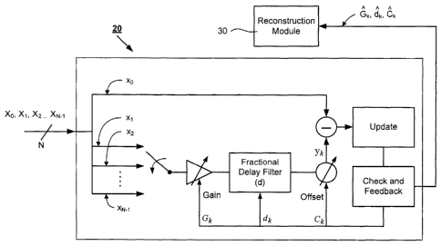
Figure 4 shows the estimation module 20 in more detail. The function of the
estimation module
20 will be further explained in connection with the flowchart in Fig. 5. Among
the N digitized
signals X0 to XN_i entering the estimation module 20 it is preferred that
signal X0 is
selected as a reference signal provided to a digital subtracter, whereas the
remaining signals
- XN_i are provided to a multiplexer. The multiplexer is adapted to multiplex
the signals
- XN_i to a variable amplifier. The amplifier is arranged to amplify or
attenuate the
CA 02655506 2014-10-01
12
signal provided by the multiplexer in a variable fashion depending on a first
input steering
value, which e.g. can be done by means of digital multiplications. The
resulting amplified or
attenuated signal is provided to a delay filter. The delay filter is arranged
to delay the provided
signal in a variable fashion depending on a third input steering value. The
delay filter is
preferably a fractional delay filter (FD-filter) adapted to delay the received
signal by fractions
of the sampling period T for the analog-to-digital converter 10. It is
particular preferred that
the fractional delay filter is a Lagrange filter or a Farrow Structure filter
or a Thiran Allpass
filter. The use of any of these filters for implementing a fractional delay
filter is favored, as its
filter response will have derivatives with respect to the delay that can be
calculated
analytically. This also further improves the numerical stability. The
resulting delayed signal is
provided to a variable offset adjuster. The offset adjuster is arranged to
provide an offset to
the received signal in a variable fashion depending on a second input steering
value, which
e.g. can be done by means of digital additions and subtractions. The first
input steering value
corresponds to a variable Gk, the second input steering value corresponds to a
variable Ck and
the third input steering value corresponds to a variable dk.
The resulting signal yk(n,dk,Gk,Ck) from the offset adjuster is provided to
the above
mentioned subtracter, which is adapted to subtract the reference signal X0
from the resulting
signal yk(n,dk,Gk,Ck). The difference yk(n,dk,Gk,Ck)-X0 is squared in a
digital squaring
module so as to create a loss-function:
no+N-1
F(dk,Gk,Ck)= E (yk(n,dk,Gk,Ck)-xo(n))2 Eq. 1
n=no
The loss-function F(dk,Gk,Ck) is in turn provided to a minimizer, which is
adapted to
estimate the channel-errors ak ,ok,ok between the reference signal X0 and a
signal Xk of
the remaining signals, X1 - XN_i, as will be further explained below.
Here, it should be emphasized that the order in which the channel-errors are
estimated can be
more or less freely chosen so as to fit the application in question. Hence,
the order in which
the channel-errors are given in equations, expressions, text and figures
herein should not be
taken as determining the order in which they are actually estimated in an
operative analog-to-
digital converter, unless it is explicitly stated that the order is essential.
CA 02655506 2014-10-01
13
Figure 5 shows a flowchart according to an embodiment of the present
invention. The
flowchart shows a detailed description of the digital signal processing steps
performed by the
error estimation module 20 in the estimation phase.
The calculations are preferably performed on batches of samples from the N
digitized signals
X0 - XN_i acquired from the N number of ADC:s in the analog-to-digital module
10. The
length of each batch of samples, M, can be selected by the skilled person, but
as an example,
1024 samples comprised by a signal X0 - XN_i is considered to be adequate.
However, in
some embodiments the calculations may be based on single samples of the N
digitized signals
X0 - XN_i. As the method is performed in a sampled system, any time period
will be
expressed in terms of the sampling period of the system. Therefore, it is
important to note that
the sampling period of the entire system is equal to the interleaving delay T
between adjacent
ADC:s, whereas the sampling period of each ADC is NT.
It should be noted, that in the present example the parallelization is used to
increase the data
rate with maintained resolution, leading to the ADC sampling period NT.
However, as the
skilled person realizes, in the case where an increase in resolution is
desired, the sampling
period of each ADC can be shorter than NT, and in the extreme case the same as
for the
system sampling period, T. This will lead to an over sampled system and a
decimation filter will
be required on the output signal.
In step S3 of the illustrated example, a loss-function F(dk,Gk,Ck) is defined
as previously
described. The loss-function F(dk,Gk,Ck) represents a relationship - e.g. a
difference -
between a reference signal X0 and the signal yk to be compared with the
reference signal
X0. In addition, the loss-function F(dk,Gk,Ck) is so defined that it can be
easily minimized
in order to determine at least one set of estimates ak , Gk, ek of the channel-
errors dk ,
Gk, Ck . The loss-function F(dk,Gk,Ck) may e.g. comprise a sum of squared
values of the
differences between the reference signal X0 and the signal yk to be compared
with the
reference signal Xo (see Eq. 1 above), or it may e.g. comprise a sum of
absolute values of
the differences between the reference signal X0 and the signal yk to be
compared with the
reference signal X0.
CA 02655506 2014-10-01
14
In step Si of the illustrated example, one of the N digitized signals Xo -
XN_i is selected as
the reference signal Xo . Here, it is assumed that the channel-errors d0,G0,C0
in the
reference signal Xo are zero and that the channel-errors dk,Gk,Ck in the other
remaining
signals X1 - XNA are relative to the channel-errors d0,G0,C0 in the reference
signal X0.
As obvious to those skilled in the art, this will not introduce any limitation
since the absolute
channel-error is not important when eliminating or reducing the channel
mismatch-errors in a
time-interleaved analog-to-digital converter. It is likewise obvious to those
skilled in the art
that any of the signals X0 - XN_i can be selected as a reference signal.
In step S2 of the illustrated example, the signal Xk is selected from the
remaining signals X1
XN-l=
In step 54 of the illustrated example, the channel-errors dk, Gk, Ck are
estimated by
optimizing the loss-function F(dk,Gk,Ck), so as to obtain estimates of the
channel-errors
, Gk, Ck, which in the illustrated example is done by minimizing the function,
i.e.:
mm F(dk,Gk,Ck) Eq. 2
dk,Gk,Ck
As can be seen from Eq. 2, this is a multivariable minimization. This
optimization problem can
be solved by conventional techniques, such as Steepest Descend (SD),
Conjugated Gradient
(CG) or similar. Since the exemplifying loss-function F(dk,Gk,Ck) in essence
is a sum of
positive factors - squares in the illustrated example - it ought to be rather
smooth, in which
case it might suffice with the aforementioned optimization procedures.
However, other
optimization procedures such as genetic algorithms might also be useful.
The optimization of the loss-function F(dk,Gk,Ck) in step S4 is preferably
performed by
means of an iterative process as schematically illustrated in Fig. 6.
Hence, in step S4a of the illustrated example, the loss-function F(dk,Gk,Ck)
is provided with
or updated with a batch of values from the reference signal Xo that was
selected in step S2
and a batch of values from the signal Xk that was selected in step S3.
CA 02655506 2014-10-01
In step S4b of the illustrated example, it is preferred that the estimation is
checked. If the
estimation is unsatisfactory it is preferred that the method proceeds to step
S4c.
In step S4c of the illustrated example, it is preferred that the estimates of
the channel-errors
, Gk, C'k are feed back, i.e. feed back to the variable amplifier, the
variable delay filter
and the variable offset adjuster in the estimator 20 respectively. The
variable amplifier, the
variable delay filter and the variable offset adjuster are then adjusted
according to the
received estimated channel-errors dk, Gk, ok so as to reduce or eliminate the
channel-
errors in the signal Xk compared to the reference signal Xo.
The variable amplifier, the variable delay filter and the variable offset
adjuster being adjusted
according to the received estimated channel-errors cii, Gk, ok are then
applied to the signal
Xk. A new set of estimated channel-errors 'clk, Gk, ak are then obtained in
step S4a by
providing or updating the loss-function F(dk,Gk,Ck) with the signal Xk being
modified by
the adjusted variable amplifier, variable delay filter and variable offset
adjuster.
Each such iteration S4a, S4b, S4c can use a new batch of samples of the signal
Xk from the
analog-to-digital module 10 or work with one single set of samples, depending
on the amount
of memory available.
In addition, it is preferred that the iterations continue until a satisfactory
estimation has been
achieved, which may e.g. be determined by the number of iterations performed
and/or by
comparing the previous set of estimated channel-errors with the new set. The
optimization
procedure may then be terminated when e.g. a certain number of iterations have
been made
and/or when the differences between a previous set and a new set of estimates
are small
enough.
When the estimation is found to be satisfactory in step S4b it is preferred
that the method
proceeds to step S5.
In step S5 of the illustrated example, a satisfactory estimation has been
achieved and the
channel-errors dk Gk, Ck or a suitable representation thereof can be
calculated from the
CA 02655506 2014-10-01
16
final estimation ilk, Gk, Ck of the channel-errors. The channel-errors dk ,
Gk, Ck or
suitable representations thereof are then provided to the reconstruction
module 30.
Suitable reconstruction modules are well known per se by those skilled in the
art. Typically
such reconstruction modules comprises the necessary offset adjuster means,
gain adjuster
means and time adjuster means, which e.g. can be implemented by means of one
ore more
filter banks. An example describing the principles behind such reconstruction
modules can be
found in the paper "Reconstruction of Nonuniformly Sampled Bandlimited Signals
by Means of
Time-Varying Discrete-Time FIR Filters", published by Hindawi Publishing
Corporation in
EURASIP Journal on Applied Signal Processing, Volume 2006, Article ID 64185,
pages 1-18.
The present invention has now been described with reference to exemplifying
embodiments.
However, the invention is not limited to the embodiments described above. On
the contrary,
the full extent of the invention is determined by the scope of the appended
claims.