Note: Descriptions are shown in the official language in which they were submitted.
CA 02656317 2009-02-27
RIM 31266-CA-PAT : 263541.00176
1
TESTBED FOR TESTING ELECTRONIC CIRCUITS AND COMPONENTS
[0001] The present invention relates generally to a testbed for testing
electronic circuits
and components.
[0002] In electronics assembly and manufacturing, a printed circuit board
(PCB) is often
used to lay down electrical circuits and to provide a base for mounting
various types of
electronic components. The circuits in the PCBs may comprise electrically
conductive
pathways traced or etched from conductive material (e.g. copper sheets) onto a
non-
conductive substrate. Multiple layers of these conductive pathways may be
separated by
alternating layers of non-conductive substrates in order to form a laminate
board that may
include many layers of circuits and non-conductive substrates.
[0003] In order to connect the circuits in one or more of the conductive
layers, via-holes
many be drilled into the laminate layers of the PCB. Once the via-hole is
formed, the
inner walls of the holes are plated with copper or another conductive material
such that
any overlapping conductive pathways located at the point of the via-hole are
electrically
connected between layers. The depth of the drilling may be controlled to
connect only
some of the layers in the PCB, or the via-hole may be drilled through the
laminate board
to provide an opening from one side of the board to the other.
[0004] Components are then placed on the PCB at predetermined connection
points
provided on the outer surfaces of the PCB in order to build various parts of
the circuit
required for the designed operation of the electronic device. Generally
speaking,
electronic components with leads are attached to the PCB at connection points
defined by
conductive landing pad extensions or connectors provided on the surface of the
PCB to
receive the component leads. For electronic components that are to be
permanently
attached to the PCB, the electrical and mechanical connections between the
component
leads and the conductive landing pad extensions may be made using a suitable
soldering
paste or compound.
[0005] Once a stage of assembly has been completed, an electronic device under
test
(DUT) may be tested on a testbed to ensure that the electrical connections and
pathways
have been properly assembled to that point. To ensure a proper test, the
testbed must be
properly configured.
CA 02656317 2009-02-27
,
RIM 31266-CA-PAT : 263541.00176
2
GENERAL
[0006] In an aspect, there may be provided a method of mounting a receptacle
for
positioning a nail in an electronic testbed board, comprising: drilling one or
more via-
holes in the testbed board; electrically connecting conductive layers at the
one or more
via-holes; and drilling a mounting through-hole for mounting a receptacle
adjacent to the
one or more via-holes and substantially perpendicular to the testbed board.
[0007] In an embodiment, the method may further comprise: mounting a
receptacle in the
mounting through-hole; and electrically connecting the mounted receptacle to
the
conductive layers at the one or more via-holes.
[0008] In an embodiment, electrically connecting the conductive layers at the
one or more
via-holes may comprise applying a conductive coating to the inner walls of the
one or
more via-holes.
[0009] In another embodiment, the method may further comprise: providing a
conductive
landing pad extension at each of the one or more via-holes, the conductive
landing pad
extension being electrically connected to the conductive layers at the one or
more via-
holes.
[0010] In another embodiment, the method may further comprise: mounting a
receptacle
in the mounting through-hole; and connecting the mounted receptacle to the
conductive
layers at the one or more via-holes via the landing pad extensions.
[0011] In another embodiment, the method may further comprise: positioning the
conductive landing pad extension at each of the one or more via-holes towards
an adjacent
mounting through-hole, with a gap provided between the conductive landing pad
extension and the mounting through-hole; mounting a receptacle in the mounting
through-
hole; and connecting the mounted receptacle to the conductive layers at the
one or more
via-holes by soldering the gap between the landing pad extension and the
mounted
receptacle.
[0012] In another embodiment, drilling one or more via-holes in the testbed
board may be
completed before drilling the mounting through-hole adjacent to the one or
more via-
holes.
[0013] In another embodiment, electrically connecting conductive layers at the
one or
more via-holes may comprise vapour depositing a coating of copper or other
conductive
material into the one or more via-holes.
CA 02656317 2009-02-27
RIM 31266-CA-PAT: 263541.00176
3
[0014] In another embodiment, drilling the mounting through-hole may be
completed
before drilling one or more adjacent via-holes in the testbed board.
[0015] In another embodiment, electrically connecting conductive layers at the
one or
more via-holes may comprise inserting a copper insert or other conductive
material into
the one or more via-holes.
[0016] In another aspect, there may be provided an electronic testbed board
for mounting
a receptacle for positioning a nail, the electronic testbed board comprising:
a mounting
through-hole for mounting a receptacle, the mounting through-hole having a
suitably
precise diameter for mounting the receptacle substantially perpendicular to
the testbed
board; one or more via-holes located adjacent the mounting through-hole, the
one or more
via-holes adapted to allow an electrical connection between any conductive
layers
provided at the one or more via-holes.
[0017] In an embodiment, the electrical connection between any conductive
layers
provided at the one or more via-holes may be provided by a coating of copper
or other
conductive material.
[0018] In another embodiment, the electronic testbed board may further
comprise: a
conductive landing pad extension provided at each of the one or more via-
holes, the
conductive landing pad extensions being electrically connected to the any
conductive
layers provided at the one or more via-holes.
[0019] In another embodiment, the conductive landing pad extensions provided
at each of
the one or more via-holes may be positioned towards the mounting through-hole,
with a
gap provided between the conductive landing pad extensions and the mounting
through-
hole.
[0020] In another embodiment, the electronic testbed board may further
comprise: a
receptacle mounted in the mounting through-hole; and an electrical conductor
closing the
gap provided between the conductive landing pad extensions and the receptacle
mounted
in the mounting through-hole.
[0021] In another embodiment, the electrical conductor may be a bead of solder
electrically connecting the conductive landing pad extensions to an exposed
base of the
receptacle mounted in the mounting through-hole.
[0022] In another embodiment, the mounting through-hole for mounting a
receptacle may
be formed by mechanical drilling with a drill bit.
CA 02656317 2009-02-27
RIM 31266-CA-PAT: 263541.00176
4
[0023] In another embodiment, the diameter of the mounting through-hole for
mounting a
receptacle may be drilled to a suitably precise diameter for mounting the
receptacle
without play.
[0024] In another aspect, there may be provided an electronic testbed,
comprising: at least
one nail in a receptacle mounted in a mounting through-hole in the electronic
testbed
board, the mounting through-hole adapted to mount the receptacle in a
substantially
perpendicular position relative to the electronic testbed; one or more via-
holes adjacent the
at least one nail in a receptacle mounted in the mounting through-hole, the
one or more
via-holes adapted to electrically connect any conductive layers at the one or
more via-
holes; and an electrical connection provided between any conductive layers at
the one or
more via-holes and the at least one nail in a receptacle mounted in the
mounting through-
hole.
BRIEF DESCRIPTION OF THE DRAWINGS
[0025] In the figures which illustrate exemplary embodiments:
FIG. 1 is a perspective view of a portion of a testbed having a plurality of
nails
provided thereon;
FIG. 2A is an enlarged perspective view of two of the nails that have been
positioned incorrectly;
FIG. 2B is a schematic cross-section of the perspective view in FIG. 2A taken
at
2B-2B;
FIG. 3 is an enlarged schematic cross-section of the base of one of the nails
of
FIGS. 2A & 2B;
FIG. 4A is a schematic cross-section of an arrangement for positioning and
aligning nails in a test bed in accordance with an embodiment;
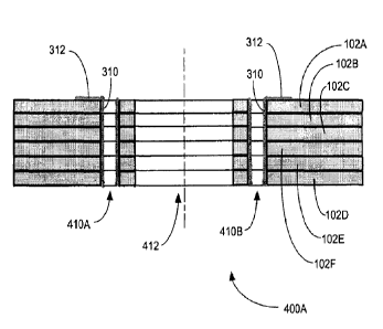
FIG. 4B is a top view of the cross-sectional view of FIG. 4A;
FIG. 4C is the schematic cross-section view of FIG. 4A of an arrangement for
electrically connecting receptacles for nails to the testbest in accordance
with another
embodiment;
FIG. 4D is a top view of the cross-sectional view of FIG. 4C; and
FIG. 5 is a schematic flowchart of a method in accordance with an embodiment.
CA 02656317 2009-02-27
. 1
RIM 31266-CA-PAT : 263541.00176
DESCRIPTION OF PREFERRED EMBODIMENTS
[0026] As noted above, the present invention relates to a testbed for testing
electronic
circuits and components.
[0027] Referring to FIG. 1, shown is a portion of a testbed platform 100 which
may be
5 used to electrically probe a DUT or device under test. As shown, this may
be achieved by
positioning a plurality of nails 110 at various locations in the testbed board
102. These
nails may be positioned at their intended locations by using receptacles 112
mounted and
soldered into position in via-holes in the testbed board 102. Each nail 110
may be spring
mounted in a receptacle 112 such that the overall height of the nails 110 as
measured from
the testbed board 102 may be adjusted for making proper contact with the probe
points of
a DUT.
[0028] In order to conduct a proper test, the testbed platform 100 must be
properly
configured, and the nails 110 must be accurately positioned within the testbed
board 102.
Heretofore, via-holes have been drilled with a larger diameter than is
necessary for the
diameter of receptacles 112, and then coated with copper or other conductive
materials to
provide an electrical connection between layers of the testbed plate 102. The
copper or
other conductive material is typically applied at the via-holes using a
metallic vapour
depositing process, and is built up to a suitable thickness to provide both an
electrical
connection at the via-holes, and a suitable diameter for the receptacles 112.
However, due
to manufacturing and processing variations, the thickness of the copper or
other
conductive material built up in the via-holes may vary. The resulting diameter
of the
copper coated via-holes may thus vary, and the via-holes may sometimes be too
large or
too small for the diameter of the receptacles 112.
[0029] Now referring to FIG. 2A and FIG. 2B, shown in FIG. 2A are illustrative
examples
of two nails 110A and 110B that have been incorrectly positioned in the
testbed board 102
for testing, as the tips of both nails 110A and 110B are significantly offset
from their
intended positions. FIG. 2B shows a cross-sectional view of FIG. 2A taken at
2B-2B,
which more clearly illustrates that the receptacles 112A and 112B are mounted
through
the via-holes 212, at slight angles from vertical.
[0030] FIG. 3 shows in more detail the incorrect positioning of receptacle
112B, in this
case due to too much play in the via-hole 212. For example, this may have
resulted from
not enough copper coating 310 being deposited on the inside surface of the via-
hole 212,
resulting in the copper coating 310 being too thin for properly positioning
the receptacle
CA 02656317 2009-02-27
RIM 31266-CA-PAT : 263541.00176
6
112B in the via-hole 212. FIG. 3B also illustrates the individual layers 102A-
102F of the
testbed board 102 that may be electrically connected by the copper coating
310.
[0031] Still referring to FIG. 3, while the angle offset of the receptacle
112B may be
slight, the tips of the nails 110A and 110B that must contact the probe points
in a DUT
(not shown) may be significantly offset from their intended locations for
probing the
DUT. This may cause inaccurate testing of a DUT placed on the testbed platform
100,
resulting in good DUTs being sent back for re-work, or even possibly bad DUTs
being
accepted and passed through.
[0032] If a bad testbed platform 100 is discovered, remedial action that may
be taken on
the testbed platform 100 often involves difficult resoldering of the nail and
receptacle, or
complete re-fabrication of the entire testbed platform which may be very
expensive.
[0033] To address the above identified problems, as will now be explained, the
inventors
have come up with a new way to mount the receptacles 112 for the nails 110 in
the testbed
board 102 which significantly improves the accuracy of the positioning of the
nails 110
for receiving and probing a DUT.
[0034] Now referring to FIG. 4A, shown is a cross-sectional view of an
arrangement for
positioning and aligning nails 110, and receptacles 112 for the nails 110 in a
testbed board
102 in accordance with an illustrative embodiment. FIG. 4B shows a
corresponding top
view of FIG. 4A, with the viewing plane of the cross-sectional view of FIG. 4A
shown in
FIG. 4B at 4A-4A. As shown, instead of having a via-hole 212 that is drilled
with a larger
diameter than is required for a receptacle, and which is then coated with
copper or other
conductive material built up to a suitable thickness, there are now a
plurality of holes that
serve different functions. More specifically, a mounting through-hole 412 is
now
provided which is precisely drilled to a suitable diameter for mounting a
receptacle 112
substantially perpendicular to the testbed board 102. Now, instead of
depositing copper or
other conductive material on the walls of through-hole 412 to provide an
electrical
connection between the layers, one or more adjacent via-holes 410A, 410B are
specifically adapted to provide an electrical connection between the layers
102A-102F,
using a copper coating 310 or a coating of another suitable conductive
material. By way
of example, in a typical embodiment, the adjacent via-holes 410A, 410B may be
drilled a
few millimeters from the through-hole 412 and should be of sufficient distance
to ensure
mechanical strength of the through-hole 412. The diameter of the via-holes
410A, 410B
should be of sufficient size to ensure that an electrical connection can be
made reliably
CA 02656317 2009-02-27
RIM 31266-CA-PAT: 263541.00176
7
through the testbed board 102. Generally speaking, the thicker the testbed
board 102, the
larger the diameter of the via-holes 410A, 410B need to be to ensure reliable
plating.
[0035] In an embodiment, drilling may encompass any technique for making a
hole that is
suitably precise to provide an accurate fit for a receptacle 112 in the
mounting through-
hole 412, such that the receptacle 112 is substantially perpendicular to the
testbed board
102. However, when drilling the testbed board 102 using a drill bit to create
the mounting
through-hole 412, it is preferable that no conductive plating should be
present where the
drill will create the mounting through-hole 412. This is because, during the
drilling of the
mounting through-hole 412, the presence of conductive plating may result in a
drill bit
possibly destroying the conductive plating, either by lifting the conductive
plating off the
board, or breaking it up, such that in either case the connection with the
opposite-side
circuit may be broken.
[0036] As the adjacent via-holes 410A and 410B no longer need to receive a
receptacle
112, the via-holes 410A and 410B may also be made smaller, and the thickness
of the
copper coating 310 may vary within a relaxed range of tolerance. Furthermore,
the via-
holes 410A and 410B need not be drilled all the way through. Instead, each of
the via-
holes 410A and 410B may be drilled to different depths, if appropriate, to
connect certain
layers 102A-102F of the testbed board 102, at possibly more than one
connection point in
each layer.
[0037] Also, suitable conductive landing pad extensions 312 may be provided at
the
location of the via-holes 410A, 410B to provide a suitable location for an
electrical
connection for the receptacles 112 or nails 110. For example, a receptacle 112
mounted in
position in the mounting through-hole 412 may be electrically connected to the
conductive
landing pad extension 312 using a lead wire and some solder (not shown).
[0038] As will be appreciated, by separating the electrical and mechanical
functions using
multiple holes 410A, 410B, 412, the accuracy in positioning the receptacles
112 (and
therefore the nails 110 mounted in place in the receptacles 112), can be
greatly improved.
That is, the receptacles 112 may be mounted in a substantially perpendicular
position
relative to the electronic testbed board 102, and without play, such that the
nails 110 can
be placed more accurately in their intended positions for contacting the probe
contact
points of a DUT. As well, as it is no longer necessary to control the
thickness of the
copper 310 as carefully as before, the success rate in manufacturing an
accurately
functioning testbed platform may also be significantly improved.
CA 02656317 2009-02-27
RIM 31266-CA-PAT : 263541.00176
8
[0039] Now referring to FIG. 4C and FIG. 4D, shown is an alternative
embodiment for
connecting the base of a receptacle (e.g. receptacle 112B) to one or more of
the via-holes
410A, 410B. As shown, the conductive landing pad extensions 312 provided at
the via-
holes 410A, 410B may be positioned towards the mounting through-hole 412.
However,
to avoid the problem of lifting the copper coating as described earlier, a
suitable clearance
or gap 430 may be provided between the conductive landing pad extension 312
and the
mounting through-hole 412. Once the mounting through-hole 412 has been
drilled, and a
receptacle 112B has been suitably positioned in the mounting through-hole 412,
a bead of
solder 420 may be provided to close the clearance 430, thereby providing an
electrical
connection between the conductive landing pad extension 312 and an exposed
base of the
receptacle 112B. Therefore, the clearance or gap 430 should be kept to a small
distance in
order to provide ease of bridging the clearance or gap with the bead of solder
420. It will
be appreciated that this way of connecting the receptacle 112B to one or more
of the via-
holes 410A, 410B avoids having to use a lead wire between the conductive
landing pad
extension 312 and the receptacle 112B. Also, the additional soldering may
provide
additional stability to the receptacle 112B mounted in the testbed board 102.
[0040] Now referring to FIG. 5, shown is a flowchart of an illustrative method
500 in
accordance with an embodiment. The processes may be, but need not be performed
in the
order shown in FIG. 5. As shown, method 500 begins and at block 502 drills one
or more
via-holes to be adjacent to a mounting through-hole.
[0041] In an embodiment, the via-holes are drilled before the mounting through-
hole is
drilled, such that at block 504 method 500 can electrically connect conductive
layers at the
via-holes. For example, the conductive layers may be electrically connected by
coating
the inner walls of one or more via-holes with copper or another conductive
coating.
Alternatively, a solid connector such as a copper insert may be inserted into
the via-holes.
[0042] Method 500 may then proceed to block 506, where method 500 provides for
each
via-hole a conductive landing pad extension electrically connected to the
conductive
layers at each via-hole. As noted earlier, in an embodiment, the conductive
landing pads
may be positioned towards the mounting through-hole with a suitable clearance.
[0043] Method 500 may then proceed to block 508, where method 500 drills the
mounting
through-hole for receiving a receptacle. As the mounting through-hole need not
go
through a conductive coating process, the diameter of the mounting through-
hole may be
CA 02656317 2012-05-07
9
drilled more precisely and substantially perpendicular to the testbed board to
accommodate the diameter of the receptacle to be mounted in the mounting
through-hole.
[0044] Method 500 may then proceed to block 510, where method 500 may
electrically
connect the receptacle to the one or more conductive landing pad extensions
using a
suitable connector. For example, the suitable connector may be a lead wire
that is bonded
to the conductive landing pad extension and to the receptacle using solder or
an ultrasonic
wire bonding machine. Alternatively, if the conductive landing pad extension
is properly
positioned towards the main thorough hole with a suitable clearance or gap
that is
provided, solder may be used to bridge the clearance or gap in order to
provide an
electrical connection between the conductive landing pad extension and a
receptacle
mounted in the mounting through-hole.
[0045] Method 500 may then proceed to block 512, where method 500 may test the
electrical connection of the receptacle (and/or the nail spring mounted in the
receptacle) to
the conductive landing pad extension and any circuits connected by the
conductive coating
in the via-holes. Method 500 then ends.
[0046] While illustrative embodiments have been described above, it will be
appreciated
that various changes and modifications may be made. More generally, the scope
of the
invention is defined by the following claims.