Note: Descriptions are shown in the official language in which they were submitted.
CA 02656509 2008-12-30
WO 2008/005782 PCT/US2007/072305
CONDUCTIVE ADHESIVE TAPE HAVING DIFFERENT ADHESION ON BOTH
SURFACES AND METHOD FOR MANUFACTURING THE SAME
BACKGROUND OF THE INVENTION
Field of the invention
The present invention relates to an electroconductive adhesive tape having
different adhesion values on both surfaces thereof and a method for
manufacturing the
same. More particularly, the present invention relates to an adhesive tape,
which has
electroconductivity along its longitudinal direction as well as on transverse
direction and
shows different adhesion values on both surfaces thereof, thus can show easy
peel-off
property if desired, and to a method for manufacturing the adhesive tape.
Description of the Prior Art
In general, the following methods have been used in order to impart
conductivity
to an adhesive tape.
First, when fabricating an adhesive, fine conductive powder such as carbon
black,
graphite, silver, copper, nickel or aluminum is uniformly distributed in the
adhesive as
conductive fillers. However, in order to impart conductivity to the adhesive
by using the
conductive fillers, particles of the conductive fillers must form a
consecutive pathway in a
polymer resin for forming the adhesive. That is, in the case of an adhesive
fabricated by a
conventional process, an excessive amount of conductive fillers are required
to impart
sufficient conductivity. However, in this case, it is difficult to uniformly
distribute
particles of carbon black, and melt viscoelasticity of an adhesive resin is
reduced, so that
filler particles may adhere with each other, thereby significantly increasing
viscosity. As a
result, the specific gravity of the resultant product is increased while
deteriorating the
physical properties of the product, so that the impact and vibration absorbing
property of
the product may be degraded. Meanwhile, even if such an excessive amount of
conductive
fillers is used, it is often difficult to obtain electroconductivity to a
sufficient degree.
Meanwhile, it is sometimes necessary to remove an adhesive from
electric/electronic products so as to attach/detach such products to/from each
other, while
not adversely affecting the products themselves, when the products are to be
discarded or
when the products are misassembled during the manufacture thereof. Also, an
adhesive
may be required to show a strong adhesion value on one surface while showing a
low
adhesion value or no adhesion value on the other surface. To accomplish this,
according to
1
CA 02656509 2008-12-30
WO 2008/005782 PCT/US2007/072305
the prior art, it has been suggested to use a substrate sheet for the
manufacture of an
adhesive tape, and then to apply an adhesive onto one surface of the substrate
sheet or to
apply different kinds of adhesives having different adhesion values onto both
surfaces
thereof.
SUMMARY OF THE INVENTION
It is an object of the present invention to provide an adhesive tape having
different adhesion values on both surfaces thereof. It is another object of
the present
invention to provide a method for imparting electroconductivity to an adhesive
tape
having different adhesion values on both surfaces thereof along its transverse
direction as
well as its longitudinal direction in order to provide more effective
conductivity to the
adhesive tape.
It is still another object of the present invention to provide an adhesive
tape,
which shows conductivity along its transverse direction as well as its
longitudinal
direction and has different adhesion values on both surfaces thereof.
It is yet another object of the present invention to provide a method for
producing
an adhesive tape, which shows conductivity along its transverse direction as
well as its
longitudinal direction and has different adhesion values on both surfaces
thereof.
The present invention provides an adhesive tape, which comprises an adhesive
polymer resin and conductive fillers distributed in the adhesive polymer
resin, and has
different adhesion values on both surfaces thereof, wherein the conductive
fillers are
aligned in both longitudinal and transverse directions in the adhesive polymer
resin while
being electrically connected with each other from one surface of the adhesive
tape to the
other surface of the adhesive tape.
The present invention also provides a method for producing an adhesive tape,
which shows conductivity along its transverse direction as well as its
longitudinal
direction and has different adhesion values on both surfaces thereof, the
method
comprising the steps of: mixing monomers for an adhesive polymer resin with
conductive
fillers; forming the resultant mixture into a sheet; and irradiating both
surfaces of the sheet
with light to perform photopolymerization of the adhesive polymer resin,
wherein the light
irradiated to each surface of the sheet has a different light intensity and
the light is
irradiated selectively to a part of the sheet surface.
The adhesive tape according to the present invention shows adhesiveness and
conductivity by itself, and thus can be used for various applications,
including
electromagnetic wave-shielding adhesives. Additionally, the adhesive tape
according to
2
CA 02656509 2008-12-30
WO 2008/005782 PCT/US2007/072305
the present invention shows a strong adhesion value on one surface so as to be
used
desirably for the purpose of housing, while having such a degree of adhesion
that it can be
removed with ease on the other surface, thereby providing excellent
workability.
BRIEF DESCRIPTION OF THE DRAWINGS
The foregoing and other objects, features and advantages of the present
invention
will become more apparent from the following detailed description when taken
in
conjunction with the accompanying drawings in which:
FIG. la is a photographic view showing the top surface (irradiated with UV
rays
under low intensity) and the bottom surface (irradiated with UV rays under
high intensity)
of an adhesive tape according to one embodiment of the present invention,
which is
obtained by irradiating each surface of an adhesive polymer resin comprising
conductive
fillers with light under different intensity;
FIG. lb is a photographic view showing the top surface and the bottom surface
of
an adhesive tape, which is obtained by irradiating both surfaces of an
adhesive resin with
light under the same intensity;
FIG. 2a is a schematic view showing fillers aligned in the adhesive tape as
shown
in FIG. l a;
FIG. 2b is a photographic view taken by a SEM (scanning electron microscope),
which shows a sectional shape of an adhesive tape and fillers aligned therein
according to
one embodiment of the present invention;
FIG. 2c is a photographic view taken by a SEM, which shows a surface of an
adhesive tape and fillers aligned therein according to one embodiment of the
present
invention;
FIG. 2d shows an example of the present invention, wherein a conductive mesh
film that is prepared by coating a conductive mesh with polymer resin is used
as a mask
having a masking pattern, and the conductive mesh film is incorporated in the
adhesive
tape.
FIG. 3 is a schematic view showing a masking pattern applicable to a release
sheet according to one embodiment of the present invention;
FIGs. 4a and 4b are schematic views showing the alignment of fillers being
changed upon the light irradiation according to one embodiment of the present
invention;
and
FIGs. 5a and 5b are graphs showing the initial adhesion (FIG. 5a) of the top
surface and the bottom surface of an adhesive tape, which is obtained by using
light with
3
CA 02656509 2008-12-30
WO 2008/005782 PCT/US2007/072305
different intensity, and the aged adhesion (FIG. 5b) thereof, measured after a
lapse of one
week at 65 C.
DETAILED DESCRIPTION OF THE INVENTION
Reference will now be made in detail to the preferred embodiments of the
present
invention.
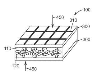
According to the present invention, the adhesive tape 100 may be produced in
the
form of a sheet. In the adhesive tape 100, the conductive fillers 120 are
aligned along the
transverse direction 130 as well as the longitudinal direction 140 of the
adhesive tape 100.
Such alignment of the conductive fillers 120 allows the conductive fillers 120
to be
connected electrically to each other from one surface of the adhesive tape 100
to the other
surface of the adhesive tape 100. That is, the conductive fillers 120 can form
a
conductive network over the whole area of the adhesive tape 100.
FIGs. 2a-2c show embodiments of the conductive fillers 120 aligned in the
adhesive tape 100 according to the present invention. The adhesive tape 100
allows
electric current to flow through the network formed by the conductive fillers
120 as shown
in FIGs. 2a-2c.
According to the present invention, in order to allow the conductive fillers
120 to
be aligned along the transverse direction 130 as well as the longitudinal
direction 140 of
the adhesive polymer resin, mobility of the fillers 120 can be utilized during
the
polymerization process. In detail, when performing the photopolymerization
process by
irradiating light 450 onto a syrup-state polymer composition 110 after adding
conductive
fillers 120 to the syrup-state polymer composition 110 (hereinafter, referred
to also as
"polymer syrup 110"), in which monomers have not yet been completely cured,
the light
450 is selectively irradiated to the surface of the polymer syrup 110 in such
a manner that
photopolymerization is selectively initiated on the surface of the polymer
syrup 110,
thereby aligning the conductive fillers 120 in a desired pattern. To
accomplish such
selective initiation of polymerization, a mask having a desired masking
pattern 310, for
example a release sheet 300 having a masking pattern 310, can be used (see
FIG. 3).
More particularly, when irradiation is performed through the mask having a
masking pattern 310, the light 450 cannot pass through the light-shielding
area formed by
the masking pattern 310 or the amount of light 450 passing through the mask
may be
significantly reduced, so that the photopolymerization is not initiated, or
the
photopolymerization speed is reduced or is very low even if the
photopolymerization may
be initiated (see FIG. 4b). However, photopolymerization may actively occur at
an area,
4
CA 02656509 2008-12-30
WO 2008/005782 PCT/US2007/072305
which is not affected by the masking pattern 310, thereby creating radicals.
As a result,
polymerization may proceed smoothly in the downward direction from the masking
pattern 310.
When polymer syrup 110 containing fillers 120 begins to be polymerized from
the surface by the light irradiation, the fillers 120 remaining in an area
where the
polymerization is initiated are shifted into an area where the polymerization
is not yet
initiated. That is, when photopolymerization proceeds from both surfaces of
the polymer
syrup 110, polymerization is initiated from the surface and the conductive
fillers 120
remaining in the surface are shifted into an internal intermediate layer where
polymerization is not yet initiated (see FIG. 4a). In contrast, since
polymerization is not
initiated in the area formed below the masking pattern 310, conductive fillers
120
remaining in the above area are not shifted downwardly (see FIG. 4b).
Accordingly, as shown in FIGs. 2a-2c, the conductive fillers 120 are
concentrated
in the central portion (when viewed from the longitudinal direction 140) of
the sheet at an
area where the masking pattern 310 is not formed, and are retained in the
longitudinal
direction 140 at an area where the masking pattern 310 is formed, thereby
forming the
conductive network over the whole area of the polymer resin sheet. That is,
the conductive
fillers 120 are aligned along the longitudinal direction 140 (z-axis
direction) of the
polymer resin sheet at the area where the masking pattern 310 is formed and
are aligned in
the intermediate layer of the polymer resin sheet along the transverse
direction 130 (x-y
plane) at the area where the masking pattern 310 is not formed, thereby
forming the
conductive network in the longitudinal and transverse directions 130 of the
adhesive
polymer sheet. Therefore, the conductive fillers 120 can be electrically
connected to each
other from one surface of the adhesive tape 100 to the other surface of the
adhesive tape
100. Thus, the adhesive tape 100 according to the present invention may have
superior
electroconductivity as compared to a conventional adhesive tape 100 in which
the
conductive fillers 120 are randomly distributed.
Additionally, when each surface of the polymer syrup 110 for forming the
adhesive tape 100 is irradiated with light 450 under different intensity, the
mobility of the
fillers 120 is changed, and thus the adhesive tape 100 has different adhesion
values on
both surfaces thereof. For example, on the surface irradiated with light 450
under higher
intensity, photopolymerization of the polymer syrup 110 proceeds more
promptly,
resulting in an increase in the mobility of the fillers 120. Thus, the fillers
120 to be aligned
in the transverse direction 130 tend to lean to the side irradiated with light
450 under lower
intensity. That is, the fillers 120 to be aligned on the x-y plane are
displaced more closely
to the surface irradiated with light 450 under lower intensity, as compared
with the surface
5
CA 02656509 2008-12-30
WO 2008/005782 PCT/US2007/072305
irradiated with light 450 under higher intensity (see FIG. 2a). In addition,
on the surface
irradiated with light 450 under higher intensity, rapid photopolymerization
occurs, and
thus the fillers 120 move rapidly, resulting in formation of surface
roughness.
Meanwhile, the adhesive polymer layer formed at the side irradiated with light
450 under higher intensity is thicker than the adhesive polymer layer formed
at the side
irradiated with light 450 under lower intensity, because the fillers 120
aligned on the x-y
plane lean to the latter side. However, the surface irradiated with light 450
under higher
intensity may have a lower adhesion value due to the aforementioned surface
roughness.
Therefore, it is possible to provide an adhesive tape 100, which has different
adhesion values on both surfaces thereof while showing electroconductivity, by
a single
manufacturing process according to the present invention.
The adhesion value on each surface of the adhesive tape 100 depends on the
particular use and target material of the adhesive tape 100. According to one
embodiment
of the present invention, one surface of the adhesive tape 100 may have an
initial adhesion
value of about 300-1000 gf/inch (116-386 centiNewtons/centimeter) and the
other surface
of the adhesive tape 100 may have an initial adhesion value of about 800-2500
gf/inch
(309-965 centiNewtons/centimeter).
Although there is no particular limitation in the thickness of the adhesive
tape
100, the adhesive tape 100 may have a thickness of about 0.2mm-3mm,
considering
photopolymerization characteristics, etc.
According to the present invention, the adhesive polymer resin may be used in
an
amount of about 10-95 wt% based on the total weight of the adhesive tape 100.
In the present invention, an acryl-based polymer resin may be used as the
adhesive polymer resin. According to a preferred embodiment of the present
invention, an
acryl-based polymer that can be obtained from the polymerization of
photopolymerizable
monomers may be used.
The photopolymerizable monomer includes alkyl acrylate monomer having a C l-
C14 alkyl group. Non-limiting examples of the alkyl acrylate monomer include
butyl
(meth)acrylate, hexyl (meth)acrylate, n-octyl (meth)acrylate, isooctyl
(meth)acrylate, 2-
3 0 ethyl-hexyl (meth)acrylate, and isononyl (meth)acrylate. In addition,
particular examples
of the alkyl acrylate monomer that may be used in the present invention also
include
isooctyl acrylate, isononyl acrylate, 2-ethyl-hexyl acrylate, decyl acrylate,
dodecyl
acrylate, n-butyl acrylate, and hexyl acrylate.
Although the alkyl acrylate monomer can form the acryl-based adhesive polymer
resin by homopolymerization, it may be copolymerized with a copolymerizable
monomer
having a polarity different from that of the alkyl acrylate monomer in order
to form the
6
CA 02656509 2008-12-30
WO 2008/005782 PCT/US2007/072305
adhesive polymer resin. That is, according to an embodiment of the present
invention, it is
also possible to use a copolymer of a C l-C l4 alkyl acrylate monomer with a
polar
copolymerizable monomer, as the acryl-based adhesive polymer resin.
Herein, there is no particular limitation in the ratio of the alkyl acrylate
monomer
to the polar copolymerizable monomer. However, a weight ratio of 99-50 : 1-50
can be
adopted, considering the physical properties of the resultant adhesive polymer
resin.
Non-limiting examples of the polar copolymerizable monomer include acrylic
acid, itaconic acid, hydroxyalkyl acrylate, cyanoalkyl acrylate, acrylamide,
substituted
acrylamide, N-vinyl pyrrolidone, N-vinyl caprolactam, acrylonitrile, vinyl
chloride, and
diallyl phthalate.
The polar copolymerizable monomer imparts adhesive and coherent properties to
the polymer resin while improving adhesion of the polymer resin.
The adhesive tape 100 according to the present invention comprises a
conductive
filler for imparting electroconductivity. Although there is no particular
limitation in kind
of the conductive filler, the conductive filler that may be used includes
noble metals; non-
noble metals; noble metal-plated noble or non-noble metals; non-noble metal-
plated noble
and non-noble metals; noble or non-noble metal plated non-metals; conductive
non-
metals; conductive polymers; and mixtures thereof. More particularly, the
conductive filler
that may include noble metals such as gold, silver, platinum; non-noble metals
such as
nickel, copper, tin, aluminum, and nickel; noble metal-plated noble or non-
noble metals
such as silver-plated copper, nickel, aluminum, tin, or gold; non-noble metal-
plated noble
and non-noble metals such as nickel-plated copper or silver; noble or non-
noble metal
plated non-metals such as silver or nickel-plated graphite, glass, ceramics,
plastics,
elastomers, or mica; conductive non-metals such as carbon black or carbon
fiber;
conductive polymers such as polyacetylene, polyaniline, polypyrrole,
polythiophene, poly
sulfumitride, poly(p-phenylene), poly(phenylene sulfide) or poly(p-
phenylenevinylene);
and mixtures thereof.
The filler is broadly classified as "particulate" in form, although the
particular
shape of such form is not considered critical to the present invention, and
may include any
shape that is conventionally involved in the manufacture or formulation of
conductive
materials of the type herein involved including hollow or solid microspheres,
elastomeric
balloons, flakes, platelets, fibers, rods, irregularly-shaped particles, or a
mixture thereof.
Similarly, the particle size of the filler is not considered critical, and may
be or a
narrow or broad distribution or range, but in one exemplary embodiment of the
present invention will be between about 0.250-250 gm, and in another exemplary
embodiment between about 1-100 fLm.
7
CA 02656509 2008-12-30
WO 2008/005782 PCT/US2007/072305
The conductive fillers 120 may be used in an amount of 5-90 wt% based on the
total weight of the adhesive tape 100 according to the present invention.
According to an
embodiment of the present invention, the adhesive tape 100 may comprise 40-80
wt% of
the adhesive polymer resin and 20-60 wt% of the conductive fillers 120.
According to
another embodiment of the present invention, the conductive fillers 120 may be
used in an
amount of 100 to 500 parts by weight based on 100 parts by weight of the
adhesive
polymer resin.
In order to obtain physical properties required for a product, to which the
adhesive tape 100 is applied, the adhesive tape 100 according to the present
invention may
further comprise at least one filler. There is no particular limitation in the
type of fillers
120, as long as the filler does not adversely affect the characteristics and
utility of the
adhesive tape 100. For instance, the fillers include, but are not limited to,
heat conductive
fillers, flame-resistant fillers, anti-static agents, foaming agents and
polymer hollow
microspheres.
According to the present invention, the fillers may be used in an amount of
less
than 100 parts by weight, for example 10-100 parts by weight, based on 100
parts by
weight of the adhesive tape 100.
In addition, the polymer resin may include other additives, such as
polymerization initiators, cross-linking agents, photo-initiators, pigments,
anti-oxidants,
UV-stabilizers, dispersants, defoaming agents, thickening agents,
plasticizers, tackifying
resins, or glazing agents.
Hereinafter, the method for producing the adhesive tape 100 according to the
present invention will be explained in more detail.
The adhesive tape 100 according to the present invention may be produced by
mixing the monomer for forming the adhesive polymer resin with conductive
fillers for
imparting conductivity, adding fillers or additives thereto if necessary, and
then carrying
out polymerization of the resultant mixture. At this time, photopolymerization
is carried
out by irradiating each surface of the adhesive polymer resin with light 450
under different
intensity, thereby providing the adhesive tape 100 having different adhesion
values on
both surfaces thereof.
In detail, the adhesive tape 100 according to the present invention, which
shows
conductivity along its longitudinal direction 140 as well as its transverse
direction 130 and
has different adhesion values on both surfaces thereof, can be produced by the
method
comprising the steps of:
3 5 mixing monomers for forming an adhesive polymer resin with conductive
fillers;
forming the mixture in the form of a sheet; and
8
CA 02656509 2008-12-30
WO 2008/005782 PCT/US2007/072305
irradiating both surfaces of the sheet with light 450 to carry out
photopolymerization of the adhesive polymer resin, wherein each surface of the
sheet is
irradiated with light 450 under different intensity and the light 450 is
irradiated selectively
to a part of the sheet surface. The method may further comprise a step of
adding
polymerization initiators or cross-linking agents.
According to one embodiment of the present invention, in order to allow the
conductive fillers 120 to be distributed uniformly and to facilitate
initiation of the
aforementioned selective photopolymerization, the monomers for forming the
adhesive
polymer resin is preliminarily polymerized to provide polymer syrup 110, and
then
conductive fillers 120 and other additives are added to the polymer syrup 110.
That is, the
step for mixing monomers for forming the adhesive polymer resin with
conductive fillers
120 may include the steps of: carrying out partial polymerization of the
monomers for
forming the adhesive polymer resin to form polymer syrup 110; and adding the
conductive
fillers 120 to the polymer syrup 110. According to an embodiment of the
present
invention, the polymer syrup 110 may have a viscosity of about 500-20,000 cps.
As mentioned above, an acryl-based polymer resin may be used as the adhesive
polymer resin.
Therefore, according to an embodiment of the present invention, the adhesive
tape 100 can be obtained by the method comprising the steps of:
2 0 carrying out partial polymerization of monomers for forming the adhesive
polymer resin to form polymer syrup 110;
adding conductive fillers 120 to the polymer syrup 110 and uniformly mixing
the
mixture;
forming the polymer syrup 110 including the conductive fillers 120 added
thereto
into a sheet and aligning a mask having a predetermined masking pattern 310 on
a surface
of the sheet; and
irradiating light 450 to the sheet through the mask to perform
photopolymerization, wherein each surface of the sheet is irradiated with
light 450 under
different intensity.
More particularly, the monomers for forming the adhesive polymer resin are
partially polymerized by using a polymerization initiator under an oxygen-free
condition
to obtain polymer syrup 110 having a viscosity of about 500 to 20,000 cps.
Then, the
conductive fillers 120, other additives, cross-linking agents and photo-
initiators are added
to the polymer syrup 110, and then the mixture is formed into a sheet, which
can be used
as a tape. At this time, the polymer syrup 110 sheet may be interposed between
release
sheets 300 by using light-transmittable release sheets 300. Such disposition
permits
9
CA 02656509 2008-12-30
WO 2008/005782 PCT/US2007/072305
formation of the condition substantially free from oxygen. Additionally, if a
masking
pattern 310 is formed on the release sheet 300, the release sheet 300 may
serve as a mask
having a masking pattern 310. Then, the sheet is irradiated with light 450
(preferably UV
rays) through the release sheet 300 or other mask having a masking pattern 310
so that the
polymer syrup 110 is polymerized and cross-linked under the condition
substantially free
from oxygen. At this time, each surface of the polymer syrup 110 is irradiated
with light
450 under different intensity in order to provide an adhesive tape 100 having
different
adhesion values on both surfaces thereof. By doing so, it is possible to
obtain an adhesive
tape 100 comprising a network formed by conductive fillers 120 and having
different
adhesion values on both surfaces thereof.
According to an embodiment of the present invention, a thixotropic material,
such as fumed silica, can be employed if necessary, in order to sufficiently
thicken the
monomers so that the monomer can form syrup.
For instance, when both surfaces of the sheet are irradiated with light 450,
oxygen content may be 1000ppm or less. As the oxygen content decreases,
undesired
oxidation of the adhesive polymer resin can be inhibited more effectively,
thereby
providing an excellent adhesion value. In other words, after the polymer syrup
110 is
interposed between release sheets 300 and the resultant mixture is formed into
a sheet, the
sheet may be irradiated with light 450 in a substantially oxygen-free chamber,
where
oxygen is present at a concentration of less than 1000ppm, through a mask
having a
masking pattern 310. If desired, it is possible to adjust the oxygen
concentration to
500ppm or less.
In the step of photopolymerization, in order to accomplish selective
irradiation on
the polymer sheet, a mask having masking pattern 310 can be used. The mask
having a
predetermined masking pattern 310 includes a light-passing area for allowing
the light 450
to pass therethrough and a light-shielding area for shielding or reducing the
light 450
passing therethrough. The mask may include, but is not limited to, a light-
transmittable
release sheet 300 having a predetermined masking pattern 310, a mesh net, a
mesh, or a
lattice. According to an embodiment of the present invention, the light-
transmittable
release sheet 300 having a predetermined masking pattern 310 may be used as
the mask
(see FIG. 3). Herein, the light-transmittable release sheet 300 that may be
used includes a
transparent plastic film treated with a release coating agent or having lower
surface
energy. For instance, the light-transmittable release sheet 300 can be
fabricated by using a
plastic film, such as a polyethylene film, a polypropylene film or a
polyethylene
terephthalate (PET) film.
Meanwhile, in order to form the masking pattern 310, a material capable of
CA 02656509 2008-12-30
WO 2008/005782 PCT/US2007/072305
masking the light 450 arriving at the masking part to a ratio of 10-100%,
preferably to a
ratio of 50% or more, may be used. According to an embodiment of the present
invention,
the masking pattern 310 may be designed in such a manner that it can shield
the light 450
arriving at the masking pattern 310 to a ratio of 70% or more. If necessary,
the masking
pattern 310 may be designed in such a manner that it can completely (100%)
shield the
light 450 arriving at the masking pattern 310.
There is no particular limitation in the method for forming the masking
pattern
310 on the surface of the light-transmittable release sheet 300. Any methods
that permit a
material for forming the masking pattern 310, which can reduce light
transmission or can
shield the light transmission, to be applied onto the light-transmittable
release sheet 300
can be used with no limitation. For example, a printing method may be used.
The printing
method includes a currently used printing method, such as a screen printing
method, a
printing method using a heat transfer sheet, or a gravure printing method. To
form the
masking pattern 310, it is also possible to use black ink having excellent
light absorptivity.
The figure of the masking pattern 310 is not limited, for example, the masking
pattern 310
shown in FIG. 3 may be adopted.
There is no particular limitation in the type of the masking pattern 310
formed in
the release sheet 300. According to an embodiment of the present invention, a
light
shielding section formed by the masking pattern 310 may occupy 1 to 70% of the
release
sheet 300. If the area of the light shielding section is less than 1% of the
release sheet 300,
the conductive fillers 120 cannot be efficiently aligned in the longitudinal
direction 140. In
contrast, if the area of the light shielding section exceeds 70% of the
release sheet 300, it
may interrupt photopolymerization.
Although there is no particular limitation in the thickness of the release
sheet 300,
a release sheet 300 having a thickness of about 5gm-2mm may be used according
to an
embodiment of the present invention. If the release sheet 300 has a thickness
of less than
5,um, the release sheet 300 is too thin to form a pattern and to apply polymer
syrup 110
thereon. It is not necessary to use a release sheet 300 having an excessively
large
thickness. This is because a release sheet 300 having a thickness of greater
than 2mm may
interrupt photopolymerization.
In one embodiment of the present invention, as a mask having masking pattern
310 for the selective irradiation, a conductive mesh film may be used. The
conductive
mesh film can be prepared by coating a conductive mesh with polymer resin. In
the
conductive mesh film, the conductive mesh does not pass light 450 therethrough
and thus
can function as a masking pattern 310; and the conductive mesh has
conductivity. The
conductive mesh film selectively shields light 450 passing through to make
selective
11
CA 02656509 2008-12-30
WO 2008/005782 PCT/US2007/072305
photopolymerization, however conductive mesh film is not removed after
photopolymerization, but is incorporated into the adhesive tape 100 to form
one side of the
adhesive tape 100. When the conductive mesh film is used, different adhesion
value can
be accomplished easily.
Thickness of the conductive mesh film is not limited, but a thickness may be
about 5X-2mm according to one embodiment of the present invention.
In addition, there is no particular limitation in the thickness of the
adhesive tape
100 according to the present invention. For instance, the adhesive tape 100
may have a
thickness of about 25,um to 3mm by taking photopolymerizability of the
monomers and
mobility of the conductive fillers 120 into consideration. If the thickness of
the adhesive
tape 100 is less than 25,um, workability may be degraded due to the thin
thickness of the
adhesive tape 100. In contrast, if the thickness of the adhesive tape 100
exceeds 3mm, it
may interrupt photopolymerization.
The light 450 has intensity adaptable for typical photopolymerization.
According
to an embodiment of the present invention, the light 450 has intensity
identical to that of
UV rays. In addition, irradiation time may be changed depending on the light
450 intensity
during the photopolymerization process. According to the present invention,
both surfaces
of the polymer syrup 110 sheet for forming the adhesive tape 100 are
irradiated with light
450 under different intensity. That is, one surface is irradiated with light
450 under
relatively high intensity, while the other surface is irradiated with light
450 under
relatively low intensity. The low intensity may be 10-90% of the high
intensity.
According to the present invention, a crosslinking agent may be used to
perform
crosslinking of the adhesive polymer resin. Properties of the adhesive polymer
resin, in
particular, adhesive property of the adhesive polymer resin can be adjusted
depending on
the amount of the cross-linking agent. For example, the cross-linking agent
may be used in
an amount of about 0.05 to 2 parts by weight based on 100 parts by weight of
the adhesive
polymer resin. Particular examples of the cross-linking agent that may be used
in the
present invention include multi-functional acrylate, such as 1,6-hexanediol
diacrylate,
trimethylopropane triacrylate, pentaerythritol triacrylate, 1,2-ethylene
glycol diacrylate, or
1,12-dodecanediol acrylate. However, the present invention is not limited
thereto.
In addition, a photo-initiator can be used during the production of the
adhesive
tape 100. The polymerization degree of the polymer resin can be adjusted
depending on
the amount of the photo-initiator. For example, the photo-initiator may be
used in an
amount of about 0.01 to 2 parts by weight based on 100 parts by weight of the
adhesive
polymer resin. Particular examples of the photo-initiator that may be used in
the present
invention include 2,4,6-trimethylbenzoyldiphenyl phosphineoxide, bis(2,4,6-
12
CA 02656509 2008-12-30
WO 2008/005782 PCT/US2007/072305
trimethylbenzoyl) phenylphosphineoxide, a,a-methoxy-a-hydroxyacetophenone, 2-
benzoyl-2(dimethyl amino)-1-[4-(4-morphonyl)phenyl]-1-butanone, or 2,2-
dimethoxy 2-
phenyl acetophenone. However, the present invention is not limited thereto.
According to an embodiment of the present invention, in order to improve
flexibility of the adhesive tape 100, the adhesive tape 100 can be subjected
to a foaming
process. The foaming process includes various foaming schemes, such as
mechanical
distribution of foam through the injection of a gaseous foaming agent,
dispersion of
hollow polymer microspheres, or use of a thermal foaming agent. Non-limiting
examples
of the foaming agent include, but are not limited to: water; volatile organic
compounds
(VOC) such as propane, n-butane, isobutane, butylene, isobutene, pentane,
neopentane or
hexane; and inert gases such as nitrogen, argon, xenon, krypton, helium, or
COz. The
foaming agent may be added to partially polymerized polymer syrup 110.
Hereinafter, the present invention will be described in detail with reference
to
examples, comparative examples and experimental examples, which are for
illustrative
purposes only and are not intended to limit the scope of the present
invention.
In the following description, the term "parts" refers to "parts by weight"
based on
100 parts by weight of the adhesive polymer resin obtained from the
polymerization of the
monomers.
<Examples 1-4 and Comparative Example 1>
First, 93 parts of 2-ethylhexyl acrylate as an acrylic monomer, 7 parts of
acrylic
acid as a polar monomer, and 0.04 parts of Irgacure-651 (a,a-methoxy-a-
hydroxyacetophenone) as a photoinitiator, were partially polymerized in a 1L
glass reactor
to obtain syrup with a viscosity of 3000 cps. Next, 100 parts of the syrup
were mixed with
0.1 part of Irgacure-819 [Bis (2,4,6-trimethylbenzoyl) phenyl-phosphineoxide]
as a
photoinitiator, 0.65 parts of 1,6-hexanediol diacrylate (HDDA) as a cross-
linking agent,
and 1.5 parts of fumed silica, and the mixture was sufficiently stirred. Then,
30 parts of
silver coated hollow glass spheres (SH230S33, Potters Industries Inc.) having
a particle
size of about 44,um were mixed with the above mixture as electroconductive
fillers, and
then the resultant mixture was stirred thoroughly to a uniform state, thereby
providing a
mixture in the form of polymer syrup.
Meanwhile, as shown in FIG. 3, the lattice having a width of 700,um and an
interval of 1.5mm was patterned on a transparent polypropylene film having a
thickness of
75,um by using black ink to provide a mask having a masking pattern in the
form of a
release sheet.
13
CA 02656509 2008-12-30
WO 2008/005782 PCT/US2007/072305
Then, the polymer syrup was extruded from the glass reactor and the patterned
release sheets were aligned on both surfaces of the polymer syrup by using a
roll coating
device in such a manner that the polymer syrup could be positioned between the
release
sheets with a thickness of about 0.5mm. Since the release sheets were aligned
on both
surfaces of the polymer syrup, the polymer syrup was prevented from contacting
with air,
especially, oxygen.
Then, UV rays were irradiated to the release sheet having the masking pattern
by
using a metal halide UV lamp under the intensity as shown in the following
Table 1 to
provide adhesive tapes, which were designated as Examples 1, 2 and 3 and
Comparative
Example 1. For convenience, UV rays with high intensity were irradiated to the
bottom
surface (B), while UV rays with low intensity were irradiated to the top
surface (T). In
Comparative Example 1, UV rays were irradiated to both of the bottom surface
and the top
surface under the same intensity.
Meanwhile, when irradiating the adhesive tapes with UV rays, each of the
adhesive tape samples according to Examples 1-3 and Comparative Example 1 was
divided into three zones (Zone 1, Zone 2 and Zone 3), and each zone was
irradiated with
UV rays under predetermined intensity.
[Table 1]
UV intensity mW/cm Line Speed Thickness
Sample Zone 1 Zone 2 Zone 3
T:B T:B T:B
Comp.Ex. 4.1 4.1 4.1 4.1 4.1 4.1 0.5 mpm (520 Sec.) 500 km
Ex. 1 2.8 4.1 2.8 4.1 2.8 4.1
Ex. 2 1.3 4.1 1.3 4.1 1.3 4.1
Ex. 3 0.2 4.1 2.8 4.1 4.1 4.1
The adhesive tapes were observed to determine the distribution of the fillers.
FIGs. 2a to 2c are photographic views taken by an SEM (scanning electron
microscope),
which show the section of the adhesive tape according to Example 1.
As shown in FIGs. 2a to 2c, the conductive fillers are aligned in the
longitudinal
direction (z-axis direction) of the adhesive polymer sheet in the area, where
the masking
pattern is formed, and are aligned in the transverse direction (x-y plane) of
the adhesive
polymer sheet at the middle portion of the adhesive polymer sheet in the area,
where the
masking pattern is not formed, thereby forming the conductive network over the
whole
area (along the x-y direction as well as the z-direction) of the adhesive
polymer sheet.
Additionally, it can be seen that the fillers aligned in the transverse
direction (x-y plane)
14
CA 02656509 2008-12-30
WO 2008/005782 PCT/US2007/072305
lean to the top surface irradiated with light under low intensity (see FIG.
2a). Herein, FIG.
1 a is a photographic view showing the top surface and the bottom surface of
the adhesive
tape obtained from Example 1 according to the present invention. FIG. lb is a
photographic view showing the top surface and the bottom surface of the
adhesive tape
obtained from Comparative Example 1.
<Experimental Example 1> Resistance Measurement
Surface resistance values were measured at the three zones of each of the
adhesive tape obtained from Examples 1-3 and Comparative Example 1, according
to the
surface probe method defined by ASTMD991, by using Kiethely 580 micro-
ohmmeter.
The average resistance of the measured values was determined as the surface
resistance of
each adhesive tape. The results are shown in the following Table 2.
[Table 2]
Sample Surface Resistance (T : B),
Ohms/sq
Comp. Ex. 1 0.44 0.48
Ex. 1 0.41 0.42
Ex. 2 0.44 0.43
Ex. 3 0.49 0.44
<Experimental Example 2> Adhesion Force Test
After laminating aluminum with each of the adhesive tape obtained from
Examples 1-3 and Comparative Example 1, adhesion force of each adhesive tape
to steel
was measured in the direction of 90 . For each adhesive tape, initial adhesion
and aged
adhesion were measured at 25 C.
Herein, the initial adhesion was defined as the adhesion value measured after
a
lapse of 20 minutes at 25 C, and the aged adhesion was defined as the adhesion
value
measured after a lapse of one week at 65 C. The results are shown in the
following Table
3. For the convenience of comparison, the same results are shown in FIGs. 5a
and 5b in a
graph form.
CA 02656509 2008-12-30
WO 2008/005782 PCT/US2007/072305
[Table 3]
Initial Adhesion Aged Adhesion
Sample (gf/inch) (gf/inch)
T:B T:B
Comp. Ex. 1 1065 1073 2457 2131
Ex.1 1051 796 2497 2310
Ex. 2 934 353 2774 88
Ex. 3 979 529 2063 506
As can be seen from the above experimental results, the adhesive tape
according
to the present invention not only shows excellent conductivity but also has
different
adhesion values on both surfaces thereof. It can be also seen that the
adhesion value at the
bottom surface decreases as the intensity of the light irradiated to the top
surface increases,
while not significantly affecting the adhesion value at the top surface.
As described above, the adhesive tape according to the present invention
includes
conductive fillers aligned in the longitudinal direction as well as the
transverse direction,
so that the adhesive tape has superior conductivity. Additionally, since the
adhesive tape
according to the present invention has different adhesion values on both
surfaces thereof,
it can be used for various applications, requiring a high adhesion value on
one side and a
low adhesion value on the other side. Thus, when the adhesive tape according
to the
present invention is used as a gasket for packing an electronic appliance, the
adhesive tape
can effectively protect the electronic components installed in the electronic
appliance, by
virtue of its impact and vibration-absorbing properties and excellent
electromagnetic
wave-shielding property.
16