Note: Descriptions are shown in the official language in which they were submitted.
CA 02656530 2008-12-29
WO 2008/005109 PCT/US2007/011812
QCO.069VPC / 051222 PATENT
METHOD OF MANUFACTURING MEMS DEVICES PROVIDING AIR GAP
CONTROL
BACKGROUND OF THE INVENTION
Field of the Invention
[0001] This invention relates to microelectromechanical systems for use as
interferometric modulators. More particularly, this invention relates to
improved methods
of manufacturing microelectromechanical system devices having different sized
cavities
between a movable element and a substrate.
Description of the Related Art
100021 Microelectromechanical systems (MEMS) include micro mechanical
elements, actuators, and electronics. Micromechanical elements may be created
using
deposition, etching, and or other micromachining processes that etch away
parts of
substrates and/or deposited material layers or that add layers to form
electrical and
electromechanical devices. One type of MEMS device is called an
interferometric
modulator. As used herein, the term interferometric modulator or
interferometric light
modulator refers to a device that selectively absorbs and/or reflects light
using the
principles of optical interference. In certain embodiments, an interferometric
modulator
may comprise a pair of conductive plates, one or both of which may be
transparent and/or
reflective in whole or part and capable of relative motion upon application of
an
appropriate electrical signal. In a particular embodiment, one plate may
comprise a
stationary layer deposited on a substrate and the other plate may comprise a
metallic
membrane separated from the stationary layer by an air gap. As described
herein in more
detail, the position of one plate in relation to another can change the
optical
interference of light incident on the interferometric modulator. Such devices
have a wide
range of applications, and it would be beneficial in the art to utilize and/or
modify the
characteristics of these types of devices so that their features can be
exploited in
improving existing products and creating new products that have not yet been
developed.
SUMMARY OF THE INVENTION
[0003) An embodiment provides for a method of making at least two types of
microelecromechanical systems (MEMS) devices, the at least two types of MEMS
CA 02656530 2008-12-29
WO 2008/005109 PCT/US2007/011812
devices having different release states after removal of sacrificial material,
the method
including providing a substrate, forming a first electrically conductive layer
over at least a
portion of the substrate, forming a first sacrificial layer over at least a
portion of the first
conductive layer, forming a plurality of electrically conductive moveable
elements over
the first sacrificial layer and forming a plurality of flexure controllers
over the substrate
configured so as to operably support the electrically conductive moveable
elements when
the sacrificial layer is removed, and where the first sacrificial layer is
removable to
thereby release the MEMS devices and form cavities having at least two gap
sizes
between the first electrically conductive layer and the movable elements.
[0004] Another embodiment provides a method of making at least two types
of interferometric modulators, the at least two types of interferometric
modulators having
different cavity depths after removal of a sacrificial material, the method
including
providing a substrate, forming an optical stack over at least a portion of the
substrate,
forming a first sacrificial material over at least a portion of the optical
stack, wherein the
sacrificial material is removable to thereby form cavities, forming a second
electrically
conductive layer over portions of the first sacrificial material, and forming
at least two
types of flexure controllers over the substrate, the flexure controllers
configured so as to
operably support the second electrically conductive layer, wherein the at
least two types of
flexure controllers comprise different sized components, the different sized
components
configured to form cavities of different depths under the portions of the
second
electrically conductive layer after removal of the first sacrificial layer.
(0005] Another embodiment provides a microelecromechanical system
(MEMS) device including a substrate, a plurality of moveable elements over the
substrate,
each moveable element separated from the substrate by a cavity, and a
plurality of flexure
controllers over the substrate configured so as to operably support the
moveable elements,
wherein the plurality of flexure controllers comprise portions of different
dimensions to
control selected flexures. The selected flexures serve to form the cavities
having at least
two gap sizes between the substrate and the plurality of movable elements.
(0006] Another embodiment provides a method of controlling a depth of a
cavity between two layers of a device that includes one or more thin film
layers, the
method including providing a substrate, forming a sacrificial layer over at
least a portion
of the substrate, forming a first layer over at least a portion of the
sacrificial layer, and
forming one or more flexure controllers over the substrate, the flexure
controllers
2
CA 02656530 2008-12-29
WO 2008/005109 PCT/US2007/011812
configured so as to operably support the first layer and to form cavities,
upon removal of
the sacrificial layer, of a depth about 30% greater or more than the depth of
the sacrificial
layer, wherein the depth is measured perpendicular to the substrate.
[0007] Another embodiment provides an unreleased microelecromechanical
system (MEMS) device that includes a substrate, a sacrificial layer over at
least a portion
of the substrate, a moveable element over the first sacrificial layer, and one
or more
flexure controllers over the substrate configured so as to operably support
the moveable
element and to form a cavity between the substrate and the movable element,
upon
removal of the sacrificial layer, of a depth about 30 percent greater or more
than the depth
of the sacrificial layer, wherein the depth is measured perpendicular to the
substrate, the
sacrificial layer being removable by etching.
[0008] Another embodiment provides a method of controlling a depth of a
cavity between two layers of a device comprising one or more thin film layers,
the method
including providing a substrate, forming a sacrificial layer over at least a
portion of the
substrate, the sacrificial layer being removable by etching, forming a first
thin film layer
over at least a portion of the sacrificial layer, and forming one or more
flexure controllers
over the substrate, the flexure controllers configured so as to operably
support the first
thin film layer and to displace the thin film layer towards the substrate,
upon removal of
the sacrificial layer.
[0009] Another embodiment provides an unreleased microelecromechanical
system (MEMS) device, that includes a substrate, a sacrificial layer over at
least a portion
of the substrate, a moveable element over the first sacrificial layer and one
or more
flexure controllers over the substrate configured so as to operably support
the moveable
element and to displace the movable element towards the substrate, upon
removal of the
sacrificial layer, the sacrificial layer being removable by etching.
BRIEF DESCRIPTION OF THE DRAWINGS
[0010] FIG. I is an isometric view depicting a portion of one embodiment of
an interferometric modulator display in which a movable reflective layer of a
first
interferometric modulator is in a relaxed position and a movable reflective
layer of a
second interferometric modulator is in an actuated position.
[0011] FIG. 2 is a system block diagram illustrating one embodiment of an
electronic device incorporating a 3x3 interferometric modulator display.
3
CA 02656530 2008-12-29
WO 2008/005109 PCT/US2007/011812
[0012] FIG. 3 is a diagram of movable mirror position versus applied voltage
for one exemplary embodiment of an interferometric modulator of FIG. 1.
[0013] FIG. 4 is an illustration of a set of row and column voltages that may
be used to drive an interferometric modulator display.
[0014] FIG. 5A illustrates one exemplary frame of display data in the 3x3
interferometric modulator display of FIG. 2.
[0015] FIG. 5B illustrates one exemplary timing diagram for row and column
signals that may be used to write the frame of FIG. 5A.
[0016] FIGS. 6A and 6B are system block diagrams illustrating an
embodiment of a visual display device comprising a plurality of
interferometric
modulators.
[0017] FIG. 7A is a cross section of the device of FIG. 1.
[0018] FIG. 7B is a cross section of an alternative embodiment of an
interferometric modulator.
[0019] FIG. 7C is a cross section of another alternative embodiment of an
interferometric modulator.
100201 FIG 7D is a cross section of yet another alternative embodiment of an
interferometric modulator.
[0021] FIG. 7E is a cross section of an additional alternative embodiment of
an interferometric modulator.
[0022] FIG. 8 is a flow diagram illustrating certain steps in an embodiment of
a method of making an interferometric modulator.
[0023] FIGS. 9A-9G are schematic cross sections illustrating certain steps in
a
process for fabricating an interferometric modulator having post support
structures.
[0024] FIGS. l0A-1OD are schematic cross sections illustrating certain-steps
in a process for fabricating an interferometric modulator having rivet support
structures.
[0025] FIG. 11 is a flow diagram illustrating certain steps in an embodiment
for fabricating an interferometric modulator having flexure controllers.
[0026] FIG. 12A-12K show cross sections of alternative embodiments of
interferometric modulators having different flexure controllers that can be
fabricated
using the method of Figure 1.1.
4
CA 02656530 2008-12-29
WO 2008/005109 PCT/US2007/011812
[0027] FIGS. 13A-13F show results of analytical studies designed to show the
effects that altering the characteristics of flexure controller structures can
have on a
deflection of a supported layer upon release of the device.
DETAILED DESCRIPTION OF THE PREFERRED EMBODIMENT
[0028] The following detailed description is directed to certain specific
embodiments of the invention. However, the invention can be embodied in a
multitude of
different ways. In this description, reference is made to the drawings wherein
like parts
are designated with like numerals throughout. As will be apparent from the
following
description, the embodiments may be implemented in any device that is
configured to
display an image, whether in motion (e.g., video) or stationary (e.g., still
image), and
whether textual or pictorial. More particularly, it is contemplated that the
embodiments
may be implemented in or associated with a variety of electronic devices such
as, but not
limited to, mobile telephones, wireless devices, personal data assistants
(PDAs), hand-
held or portable computers, GPS receivers/navigators, cameras, MP3 players,
cameorders,
game consoles, wrist watches, clocks, calculators, television monitors, flat
panel displays,
computer monitors, auto displays (e.g., odometer display, etc.), cockpit
controls and/or
displays, display of camera views (e.g., display of a rear view camera in a
vehicle),
electronic photographs, electronic billboards or signs, projectors,
architectural structures,
packaging, and aesthetic structures (e.g., display of images on a piece of
jewelry). MEMS
devices of similar structure to those described herein can also be used in non-
display
applications such as in electronic switching devices.
[0029] An embodiment provides methods of making MEMS devices with a
plurality of flexure controllers over a substrate. The flexure controllers are
configured so
as to operably support electrically conductive moveable elements and to
provide a
plurality of selected flexures when a sacrificial layer is removed. The
sacrificial layer is
removable to thereby release the MEMS devices and form cavities having at
least two gap
sizes. The flexure controllers can effectuate increases in gap size as well as
decreases in
gap sizes. As a result, multiple depositions, masking and etching steps may be
replaced
by fewer deposition, masking and etching steps, thus saving time and money in
the
manufacture of MEMS devices.
[0030] One interferometric modulator display embodiment comprising an
interferometric MEMS display element is illustrated in Figure 1. In these
devices, the
CA 02656530 2008-12-29
WO 2008/005109 PCT/US2007/011812
pixels are in either a bright or dark state. In the bright ("on" or "open")
state, the display
element reflects a large portion of incident visible light to a user. When in
the dark ("off'
or "closed") state, the display element reflects little incident visible light
to the user.
Depending on the embodiment, the light reflectance properties of the "on" and
"off' states
may be reversed. MEMS pixels can be configured to reflect predominantly at
selected
colors, allowing for a color display in addition to black and white.
[0031] Figure 1 is an isometric view depicting two adjacent pixels in a series
of pixels of a visual display, wherein each pixel comprises a MEMS
interferometric
modulator. In some embodiments, an interferometric modulator display comprises
a
rowJcolumn array of these interferometric modulators. Each interferometric
modulator
includes a pair of reflective layers positioned at a variable and controllable
distance from
each other to form a resonant optical cavity with at least one variable
dimension. In one
embodiment, one of the reflective layers may be moved between two positions.
In the
first position, referred to herein as the relaxed position, the movable
reflective layer is
positioned at a relatively large distance from a fixed partially reflective
layer. In the
second position, referred to herein as the actuated position, the movable
reflective layer is
positioned more closely adjacent to the partially reflective layer. Incident
light that
reflects from the two layers interferes constructively or destructively
depending on the
position of the movable reflective layer, producing either an overall
reflective or non-
reflective state for each pixel.
[0032] The depicted portion of the pixel array in Figure 1 includes two
adjacent interferometric modulators 12a and 12b. In the interferometric
modulator 12a on
the left, a movable reflective layer 14a is illustrated in a relaxed position
at a
predetermined distance from an optical stack 16a, which includes a partially
reflective
layer. In the interferometric modulator 12b on the right, the movable
reflective layer 14b
is illustrated in an actuated position adjacent to the optical stack 16b.
[0033] The optical stacks 16a and 16b (collectively referred to as optical
stack
16), as referenced herein, typically comprise of several fused layers, which
can include an
electrode layer, such as indium tin oxide (ITO), a partially reflective layer,
such as
chromium, and a transparent dielectric. The optical stack 16 is thus
electrically
conductive, partially transparent and partially reflective, and may be
fabricated, for
example, by depositing one or more of the above layers onto a transparent
substrate 20.
The partially reflective layer can be formed from a variety of materials that
are partially
6
CA 02656530 2008-12-29
WO 2008/005109 PCT/US2007/011812
reflective such as various metals, semiconductors, and dielectrics. The
partially reflective
layer can be formed of one or more layers of materials, and each of the layers
can be
formed of a single material or a combination of materials.
[0034] In some embodiments, the layers of the optical stack are patterned into
parallel strips, and may form row electrodes in a display device as described
further
below. The movable reflective layers 14a, 14b may be formed as a series of
parallel
strips of a deposited metal layer or layers (orthogonal to the row electrodes
of 16a, 16b)
deposited on top of posts 18 and an intervening sacrificial material deposited
between the
posts 18. When the sacrificial material is etched away, the movable reflective
layers 14a,
14b are separated from the optical stacks 16a, 16b by a defined gap 19. A
highly
conductive and reflective material such as aluminum may be used for the
reflective layers
14, and these strips may form column electrodes in a display device.
[0035] With no applied voltage, the cavity 19 remains between the movable
reflective layer l4a and optical stack 16a, with the movable reflective layer
14a in a
mechanically relaxed state, as illustrated by the pixel 12a in Figure 1.
However, when a
potential difference is applied to a selected row and column, the capacitor
formed at the
intersection of the row and column electrodes at the corresponding pixel
becomes
charged, and electrostatic forces pull the electrodes together. If the voltage
is high
enough, the movable reflective layer 14 is deformed and is forced against the
optical stack
16. A dielectric layer (not illustrated in this Figure) within the optical
stack 16 may
prevent shorting and control the separation distance between layers 14 and 16,
as
illustrated by pixel 12b on the right in Figure 1. The behavior is the same
regardless of
the polarity of the applied potential difference. In this way, row/column
actuation that can
control the reflective vs. non-reflective pixel states is analogous in many
ways to that used
in conventional LCD and other display technologies.
[0036] Figures 2 through 5B illustrate one exemplary process and system for
using an array of interferometric modulators in a display application.
[0037] Figure 2 is a system block diagram illustrating one embodiment of an
electronic device that may incorporate aspects of the invention. In the
exemplary
embodiment, the electronic device includes a processor 21 which may be any
general
purpose single- or multi-chip microprocessor such as an ARM, Pentium , Pentium
II ,
Pentium III , Pentium IV , Pentium Pro, an 8051, a MIPS , a Power PC , an
ALPHA ,
or any special purpose microprocessor such as a digital signal processor,
microcontroller,
7
CA 02656530 2008-12-29
WO 2008/005109 PCT/US2007/011812
or a programmable gate array. As is conventional in the art, the processor 21
may be
configured to execute one or more software modules. In addition to executing
an
operating system, the processor may be configured to execute one or more
software
applications, including a web browser, a telephone application, an email
program, or any
other software application.
[0038J In one embodiment, the processor 21 is also configured to
communicate with an array driver 22. In one embodiment, the array driver 22
includes a
row driver circuit 24 and a column driver circuit 26 that provide signals to a
display-array
or panel 30. The cross section of the array illustrated in Figure 1 is shown
by the lines 1-1
in Figure 2. For MEMS interferometric modulators, the row/column actuation
protocol
may take advantage of a hysteresis property of these devices illustrated in
Figure 3. It
may require, for example, a 10 volt potential difference to cause a movable
layer to
deform from the relaxed state to the actuated state. However, when the voltage
is reduced
from that value, the movable layer maintains its state as the voltage drops
back below 10
volts. In the exemplary embodiment of Figure 3, the movable layer does not
relax
completely until the voltage drops below 2 volts. There is thus a range of
voltage, about 3
to 7 V in.the example illustrated in Figure 3, where there exists a window of
applied
voltage within which the device is stable in either the relaxed or actuated
state. This is
referred to herein as the "hysteresis window" or "stability window." For a
display array
having the hysteresis characteristics of Figure 3, the row/column actuation
protocol can be
designed such that during row strobing, pixels in the strobed row that are to
be actuated
are exposed to a voltage difference of about 10 volts, and pixels that are to
be relaxed are
exposed to a voltage difference of close to zero volts. After the strobe, the
pixels are
exposed to a steady state voltage difference of about 5 volts such that they
remain in
whatever state the row strobe put them in. After being written, each pixel
sees a potential
difference within the "stability window" of 3-7 volts in this example. This
feature makes
the pixel design illustrated in Figure 1 stable under the same applied voltage
conditions in
either an actuated or relaxed pre-existing state. Since each pixel of the
interferometric
modulator, whether in the actuated or relaxed state, is essentially a
capacitor formed by
the fixed and moving reflective layers, this stable state can be held at a
voltage within the
hysteresis window with almost no power dissipation. Essentially no current
flows into the
pixel if the applied potential is fixed.
8
CA 02656530 2008-12-29
WO 2008/005109 PCT/US2007/011812
[0039) In typical applications, a display frame may be created by asserting
the
set of column electrodes in accordance with the desired set of actuated pixels
in the first
row. A row pulse is then applied to the row 1 electrode, actuating the pixels
corresponding to the asserted column lines. The asserted set of column
electrodes is then
changed to correspond to the desired set of actuated pixels in the second row.
A pulse is
then applied to the row 2 electrode, actuating the appropriate pixels in row 2
in
accordance with the asserted column electrodes. The row 1 pixels are
unaffected by the
row 2 pulse, and remain in the state they were set to during the row 1 pulse.
This may be
repeated for the entire series of rows in a sequential fashion to produce the
frame.
Generally, the frames are refreshed and/or updated with new display data by
continually
repeating this process at some desired number of frames per second. A wide
variety of
protocols for driving row and column electrodes of pixel arrays to produce
display frames
are also well known and may be used in conjunction with the present invention.
[00401 Figures 4, 5A, and 5B illustrate one possible actuation protocol for
creating a display frame on the 3x3 array of Figure 2. Figure 4 illustrates a
possible set of
column and row voltage levels that may be used for pixels exhibiting the
hysteresis curves
of Figure 3. In the Figure 4 embodiment, actuating a pixel involves setting
the
appropriate column to -Vbias, and the appropriate row to +OV, which may
correspond to -
volts and +5 volts respectively Relaxing the pixel is accomplished by setting
the
appropriate column to +Vbias, and the appropriate row to the same +OV,
producing a zero
volt potential difference across the pixel. In those rows where the row
voltage is held at
zero volts, the pixels are stable in whatever state they were originally in,
regardless of
whether the column is at +Vbias, or -Vbias= As is also illustrated in Figure
4, it will be
appreciated that voltages of opposite polarity than those described above can
be used, e.g.,
actuating a pixel can involve setting the appropriate column to +Vb;as, and
the appropriate
row to -AV. In this embodiment, releasing the pixel is accomplished by setting
the
appropriate column to -Vbias, and the appropriate row to the same -OV,
producing a zero
volt potential difference across the pixel.
[00411 Figure 5B is a timing diagram showing a series of row and column
signals applied to the 3x3 array of Figure 2 which will result in the display
arrangement
illustrated in Figure 5A, where actuated pixels are non-reflective. Prior to
writing the
frame illustrated in Figure 5A, the pixels can be in any state, and in this
example, all the
9
CA 02656530 2008-12-29
WO 2008/005109 PCT/US2007/011812
rows are at 0 volts, and all the columns are at +5 volts. With these applied
voltages, all
pixels are stable in their existing actuated or relaxed states.
[0042] In the Figure 5A frame, pixels (1,1), (1,2), (2,2), (3,2) and (3,3) are
actuated. To accomplish this, during a "line time" for row 1, columns 1 and 2
are set to -5
volts, and column 3 is set to +5 volts. This does not change the state of any
pixels,
because all the pixels remain in the 3-7 volt stability window. Row 1 is then
strobed with
a pulse that goes from 0, up to 5 volts, and back to zero. This actuates the
(1,1) and (1,2)
pixels and relaxes the (1,3) pixel. No other pixels in the array are affected.
To set row 2
as desired, column 2 is set to -5 volts, and columns 1 and 3 are set to +5
volts. The same
strobe applied to row 2 will then actuate pixel (2,2) and relax pixels (2,1)
and (2,3).
Again, no other pixels of the array are affected. Row 3 is similarly set by
setting columns
2 and 3 to -5 volts, and column 1 to +5 volts. The row 3 strobe sets the row 3
pixels as
shown in Figure 5A. After writing the frame, the row potentials are zero, and
the column
potentials can remain at either +5 or -5 volts, and the display is then stable
in the
arrangement of Figure 5A. It will be appreciated that the same procedure can
be
employed for arrays of dozens or hundreds of rows and columns. It will also be
appreciated that the timing, sequence, and levels of voltages used to perform
row and
column actuation can be varied widely within the general principles outlined
above, and
the above example is exemplary only, and any actuation voltage method can be
used with
the systems and methods described herein.
[0043) Figures 6A and 6B are system block diagrams illtistrating an
embodiment of a display device 40. The display device 40 can be, for example,
a cellular
or mobile telephone. However, the same components of display device 40 or
slight
variations thereof are also illustrative of various types of display devices
such as
televisions and portable media players.
[0044] The display device 40 includes a housing 41, a display 30, an antenna
43, a speaker 45, an input device 48, and a microphone 46. The housing 41 is
generally
formed from any of a variety of manufacturing processes as are well known to
those of
skill in the art, including injection molding, and vacuum forming. In
addition, the
housing 41 may be made from any of a variety of materials, including but not
limited to
plastic, metal, glass, rubber, and ceramic, or a combination thereof. In one
embodiment
the housing 41 includes removable portions (not shown) that may be
interchanged with
CA 02656530 2008-12-29
WO 2008/005109 PCT/US2007/011812
other removable portions of different color, or containing different logos,
pictures, or
symbols.
[0045] The display 30 of exemplary display device 40 may be any of a variety
of displays, including a bi-stable display, as described herein. In other
embodiments, the
display 30 includes a flat-panel display, such as plasma, EL, OLED, STN LCD,
or TFT
LCD as described above, or a non-flat-panel display, such as a CRT or other
tube device,
as is well known to those of skill in the art. However, for purposes of
describing the
present embodiment, the display 30 includes an interferometric modulator
display, as
described herein.
[0046] The components of one embodiment of exemplary display device 40
are schematically illustrated in Figure 6B. The illustrated exemplary display
device 40
includes a housing 41 and can include additional components at least partially
enclosed
therein. For example, in one embodiment, the exemplary display device 40
includes a
network interface 27 that includes an antenna 43 which is coupled to a
transceiver 47.
The transceiver 47 is connected to a processor 21, which is connected to
conditioning
hardware 52. The conditioning hardware 52 may be configured to condition a
signal (e.g.
filter a signal). The conditioning hardware 52 is connected to a speaker 45
and a
microphone 46. The processor 21 is also connected to an input device 48 and a
driver
controller 29. The driver controller 29 is coupled to a frame buffer 28, and
to an array
driver 22, which in turn is coupled to a display array 30. A power supply 50
provides
power to all components as required by the particular exemplary display device
40 design.
[0047] The network interface 27 includes the antenna 43 and the transceiver
47 so that the exemplary display device 40 can communicate with one ore more
devices
over a network. In one embodiment the network interface 27 may also have some
processing capabilities to relieve requirements of the processor 21. The
antenna 43 is any
antenna known to those of skill in the art for transmitting and receiving
signals. In one
embodiment, the antenna transmits and receives RF signals according to the
IEEE 802.11
standard, including IEEE 802.11(a), (b), or (g). In another embodiment, the
antenna
transmits and receives RF signals according to the BLUETOOTH standard. In the
case of
a cellular telephone, the antenna is designed to receive CDMA, GSM, AMPS or
other
known signals that are used to communicate within a wireless cell phone
network. The
transceiver 47 pre-processes the signals received from the antenna 43 so that
they may be
received by and further manipulated by the processor 21. The transceiver 47
also
11
CA 02656530 2008-12-29
WO 2008/005109 PCT/US2007/011812
processes signals received from the processor 21 so that they may be
transmitted from the
exemplary display device 40 via the antenna 43.
[0048] In an alternative embodiment, the transceiver 47 can be replaced by a
receiver. In yet another alternative embodiment, network interface 27 can be
replaced by
an image source, which can store or generate image data to be sent to the
processor 21.
For example, the image source can be a memory device such as a digital video
disc
(DVD) or a hard-disc drive that contains image data, or a software module that
generates
image data.
[0049] Processor 21 generally controls the overall operation of the exemplary
display device 40. The processor 21 receives data, such as compressed image
data from
the network interface 27 or an image source, and processes the data into raw
image data
or into a format that is readily processed into raw image data. The processor
21 then
sends the processed data to the driver controller 29 or to frame buffer 28 for
storage. Raw
data typically refers to the information that identifies the image
characteristics at each
location within an image. For example, such image characteristics can include
color,
saturation, and gray-scale level.
[0050] In one embodiment, the processor 21 includes a microcontroller, CPU,
or logic unit to control operation of the exemplary display device 40.
Conditioning
hardware 52 generally includes amplifiers and filters for transmitting signals
to the
speaker 45, and for receiving signals from the microphone 46. Conditioning
hardware 52
may be discrete components within the exemplary display device 40, or may be
incorporated within the processor 21 or other components.
[0051] The driver controller 29 takes the raw image data generated by the
processor 21 either directly from the processor 21 or from the frame buffer 28
and
reformats the raw image data appropriately for high speed transmission to the
array driver
22. Specifically, the driver controller 29 reformats the raw image data into a
data flow
having a raster-like fonnat, such that it has a time order suitable for
scanning across the
display array 30. Then the driver controller 29 sends the formatted
information to the
array driver 22. Although a driver controller 29, such as a LCD controller, is
often
associated with the system processor 21 as a stand-alone Integrated Circuit
(IC), such
controllers may be implemented in many ways. They may be embedded in the
processor
21 as hardware, embedded in the processor 21 as software, or fully integrated
in hardware
with the array driver 22.
12
CA 02656530 2008-12-29
WO 2008/005109 PCT/US2007/011812
[00521 Typically, the array driver 22 receives the formatted information from
the driver controller 29 and reformats the video data into a parallel set of
waveforms that
are applied many times per second to the 'hundreds and sometimes thousands of
leads
coming from the display's x-y matrix of pixels.
[0053] In one embodiment, the driver controller 29, array driver 22, and
display array 30 are appropriate for any of the types of displays described
herein. For
example, in one embodiment, driver controller 29 is a conventional display
controller or a
bi-stable display controller (e.g., an interferometric modulator controller).
In another
embodiment, array driver 22 is a conventional driver or a bi-stable display
driver (e.g., an
interferometric modulator display). In one embodiment, a driver controller 29
is
integrated with the array driver 22. Such an embodiment is common in highly
integrated
systems such as cellular phones, watches, and other small area displays. In
yet another
embodiment, display array 30 is a typical display array or a bi-stable display
array (e.g., a
display including an array of interferometric modulators).
[0054] The input device 48 allows a user to control the operation of the
exemplary display device 40. In one embodiment, input device 48 includes a
keypad,
such as a QWERTY keyboard or a telephone keypad, a button, a switch, a touch-
sensitive
screen, a pressure- or heat-sensitive membrane. In one embodiment, the
microphone 46 is
an input device for the exemplary display device 40. When the microphone 46 is
used to
input data to the device, voice commands may be provided by a user for
controlling
operations of the exemplary display device 40.
[0055] Power supply 50 can include a variety of energy storage devices as are
well known in the art. For example, in one embodiment, power supply 50 is a
rechargeable battery, such as a nickel-cadmium battery or a lithium ion
battery. In
another embodiment, power supply 50 is a renewable energy source, a capacitor,
or a
solar cell, including a plastic solar cell, and solar-cell paint. In another
embodiment,
power supply 50 is configured to receive power from a wall outlet.
(0056] In some implementations control programmability resides, as described
above, in a driver controller which can be located in several places in the
electronic
display system. In some cases control programmability resides in the array
driver 22.
Those of skill in the art will recognize that the above-described optimization
may be
implemented in any number of hardware and/or software components and in
various
configurations.
13
CA 02656530 2008-12-29
WO 2008/005109 PCT/US2007/011812
[0057] The details of the structure of interferometric modulators that operate
in accordance with the principles set forth above may vary widely. For
example, Figures
7A-7E illustrate five different embodiments of the movable reflective layer 14
and its
supporting structures. Figure 7A is a cross section of the embodiment of
Figure 1, where
a strip of metal material 14 is deposited on orthogonally extending supports
18. In Figure
7B, the moveable reflective layer 14 is attached to supports at the corners
only, on tethers
32. In Figure 7C, the moveable reflective layer 14 is suspended from a
deformable layer
34, which may comprise a flexible metal. The deformable layer 34 connects,
directly or
indirectly, to the substrate 20 around the perimeter of the deformable layer
34. These
connections are herein referred to as support posts. The embodiment
illustrated in Figure
7D has support post plugs 42 upon which the deformable layer 34 rests. The
movable
reflective layer 14 remains suspended over the cavity, as in Figures 7A-7C,
but the
deformable layer 34 does not form the support posts by filling holes between
the
deformable layer 34 and the optical stack 16. Rather, the support posts are
formed of a
planarization material, which is used to form support post plugs 42. The
embodiment
illustrated in Figure 7E is based on the embodiment shown in Figure 7D, but
may also be
adapted to work with any of the embodiments illustrated in Figures 7A-7C as
well as
additional embodiments not shown. In the embodiment shown in Figure 7E, an
extra
layer of metal or other conductive material has been used to form a bus
structure 44. This
allows signal routing along the back of the interferometric modulators,
eliminating a
number of electrodes that may otherwise have had to be formed on the substrate
20.
[0058] In embodiments such as those shown in Figure 7, the interferometric
modulators function as direct-view devices, in which images are viewed from
the front
side of the transparent substrate 20, the side opposite to that upon which the
modulator is
arranged. In these embodiments, the reflective layer 14 optically shields the
portions of
the interferometric modulator on the side of the reflective layer opposite the
substrate 20,
including the deformable layer 34. This allows the shielded areas to be
configured and
operated upon without negatively affecting the image quality. Such shielding
allows the
bus structure 44 in Figure 7E, which provides the ability to separate the
optical properties
of the modulator from the electromechanical properties of the modulator, such
as
addressing and the movements that result from that addressing. This separable
modulator
architecture allows the structural design and materials used for the
electromechanical
aspects and the optical aspects of the modulator to be selected and to
function
14
CA 02656530 2008-12-29
WO 2008/005109 PCT/US2007/011812
independently of each other. Moreover, the embodiments shown in Figures 7C-7E
have
additional benefits deriving from the decoupling of the optical properties of
the reflective
layer 14 from its mechanical properties, which are carried out by the
deformable layer 34.
This allows the structural design and materials used for the reflective layer
14 to be
optimized with respect to the optical properties, and the structural design
and materials
used for the deformable layer 34 to be optimized with respect to desired
mechanical
properties.
[0059] Figure 8 is a flow diagram illustrating certain steps in an embodiment
of a manufacturing process 800 for an interferometric modulator. Such steps
may be
present in a process for manufacturing, e.g., interferometric modulators of
the general
type illustrated in Figures 1 and 7, along with other steps not shown in
Figure 8. With
reference to Figures 1, 7 and 8, the process 800 begins at step 805 with the
formation of
the optical stack 16 over the substrate 20. The substrate 20 may be a
transparent substrate
such as glass or plastic and may have been subjected to prior preparation
step(s), e.g.,
cleaning, to facilitate efficient formation of the optical stack 16. As
discussed above, the
optical stack 16 is electrically conductive, partially transparent and
partially reflective,
and may be fabricated, for example, by depositing one or more of the layers
onto the
transparent substrate 20. In some embodiments, the layers are patterned into
parallel
strips, and may form row electrodes in a display device. In some embodiments,
the
optical stack 16 includes an insulating or dielectric layer that is deposited
over one or
more metal layers (e.g., reflective and/or conductive layers).
[0060] The process 800 illustrated in Figure 8 continues at step 810 with the
formation of a sacrificial layer over the optical stack 16. The sacrificial
layer is later
removed (e.g., at step 825) to form the cavity 19 as discussed below and thus
the
sacrificial layer is not shown in the resulting interferometric modulator 12
illustrated in
Figures 1 and 7. The formation of the sacrificial layer over the optical stack
16 may
include deposition of a XeF2-etchable material suah as molybdenum or amorphous
silicon, in a thickness selected to provide, after subsequent removal, a
cavity 19 having
the desired size. Deposition of the sacrificial material may be carried out
using deposition
techniques such as physical vapor deposition (PVD, e.g., sputtering), plasma-
enhanced
chemical vapor deposition (PECVD), thermal chemical vapor deposition (thermal
CVD),
or spin-coating.
CA 02656530 2008-12-29
WO 2008/005109 PCT/US2007/011812
100611 The process 800 illustrated in Figure 8 continues at step 815 with the
formation of a support structure e.g., a post 18 as illustrated in Figures 1
and 7 or a rivet
as discussed below. The formation of the post 18 may include the steps of
patterning the
sacrificial layer to form a support structure aperture, then depositing a
material (e.g., a
polymer or silicon dioxide) into the aperture to form the post 18, using a
deposition
method such as PECVD, thermal CVD, or spin-coating. In some embodiments, the
support structure aperture formed in the sacrificial layer extends through
both the
sacrificial layer and the optical stack 16 to the underlying substrate 20, so
that the lower
end of the post 18 contacts the substrate 20 as illustrated in Figure 7A. In
other
embodiments, the aperture formed in the sacrificial layer extends through the
sacrificial
layer, but not through the optical stack 16. For example, Figure 7C
illustrates the lower
end of the support post plugs 42 in contact with the optical stack 16. More
detailed
discussions of other embodiments providing for formation of posts and rivets
are
presented below.
[0062] The process 800 illustrated in Figure 8 continues at step 820 with the
formation of a movable reflective layer such as the movable reflective layer
14 illustrated
in Figures 1 and 7. The movable reflective layer 14 may be formed by employing
one or
more deposition steps, e.g., reflective layer (e.g., aluminum, aluminum alloy)
deposition,
along with one or more patterning, masking, and/or etching steps. As discussed
above,
the movable reflective layer 14 is typically electrically conductive, and may
be referred to
herein as an electrically conductive layer. Since the sacrificial layer is
still present in the
partially fabricated interferometric modulator formed at step 820 of the
process 800, the
movable reflective layer 14 is typically not movable at this stage. A
partially fabricated
interferometric modulator that contains a sacrificial layer may be referred to
herein as an
"unreleased" interferometric modulator.
[0063] The process 800 illustrated in Figure 8 continues at step 825 with the
formation of a cavity, e.g., a cavity 19 as illustrated in Figures 1 and 7.
The cavity 19 may
be formed by exposing the sacrificial material (deposited at step 810) to an
etchant. For
example, an etchable sacrificial material such as molybdenum or amorphous
silicon may
be removed by dry chemical etching, e.g., by exposing the sacrificial layer to
a gaseous or
vaporous etchant, such as vapors derived from solid xenon difluoride (XeF2)
for a period
r
of time that is effective to remove the desired amount of material, typically
selectively
relative to the structures surrounding the cavity 19. Other etching methods,
e.g. wet
16
CA 02656530 2008-12-29
WO 2008/005109 PCT/US2007/011812
etching and/or plasma etching, may also be used. Since the sacrificial layer
is removed
during step 825 of the process 800, the movable reflective layer 14 is
typically movable
after this stage. After removal of the sacrificial material, the resulting
fully or partially
fabricated interferometric modulator may be referred to herein as a "released"
interferometric modulator.
[0064] In one embodiment, support structures may take the form of post
structures (e.g., posts 18 shown in Figures 1 and 7) underlying the movable
layer. An
exemplary process for fabricating an interferometric modulator comprising
support posts
is discussed with respect to Figures 9A-9G. In various embodiments,
fabricating an
interferometric modulator comprises forming an optical stack on a substrate,
which may
be a light-transmissive substrate, and in further embodiments is a transparent
substrate.
The optical stack may comprise a conductive layer, which forms an electrode
layer on or
adjacent the substrate; a partially reflective layer, which reflects some
incident light while
permitting some light to reach the other components of the interferometric
modulator
element; and a dielectric layer, which insulates the underlying electrode
layer from the
other components of the interferometric modulator. In Figure 9A, it can be
seen that a
transparent substrate 100 is provided, and that a conductive layer 102 and a
partially
reflective layer 104 are deposited over the substrate 100. A dielectric layer
106 is then
deposited over the partially reflective layer 104. In some embodiments, the
conductive
layer 102 is transparent and comprises ITO, the partially reflective layer 104
comprises a
semireflective thickness of metal, such as chromium (Cr), and the dielectric
layer 106
comprises silicon oxide (Si02). The dielectric layer may also be a stack
comprising Si02
and A1203. At some point during this process, at least the conductive layer
102 is
patterned (not shown) to form row electrodes which will be used to address a
row of
interferometric modulators. In one embodiment, this patterning takes place
after the
deposition of the conductive and partially reflective layers 102 and 104, but
prior to the
deposition of the dielectric layer 106. The combination of the layers 102,
104, and 106 is
referred to as the optical stack 110, and may be indicated by a single layer
in later figures,
for convenience. It will be understood that the composition of the optical
stack 110 may
vary both in the number of layers and the components of those layers, and that
the layers
discussed above are merely exemplary.
[0065] A variety of methods can be used to perform the patterning and etching
processes discussed with respect to the various embodiments disclosed herein.
The etches
17
CA 02656530 2008-12-29
WO 2008/005109 PCT/US2007/011812
used may be either a dry etch or a wet etch, and may be isotropic or
anisotropic. Suitable
dry etches include, but are not limited to: SF6/02, CHF3/02, SF2/02, CF4/02,
and NF3/02.
Generally, these etches are suitable for etching one or more of SiO,', SiNX,
SiOxNy, spin-
on glass, Nissan Hard coat, and TaO, but other materials may also be etched by
this
process. Materials which are resistant to one or more of these etches, and may
thus be
used as etch barrier layers, include but are not limited to Al, Cr, Ni, and
A1203. In
addition, wet etches including but not limited to PAD etches, BHF, KOH, and
phosphoric
acid may be utilized in the processes described herein. Generally, these
etches may be
isotropic, but can be made anisotropic through the use of a reactive ion etch
(RIE), by
ionizing the etch chemicals and shooting the ions at the substrate. The
patterning may
comprise the deposition of a photoresist (PR) layer (either positive or
negative
photoresist), which is then used to fonm a mask. Alternately, a hard mask can
be utilized.
In some embodiments, the hard mask may comprise metal or SiNx, but it will be
understood that the composition of the hard mask may depend on the underlying
materials
to be etched and the selectivity of the etch to be used. In The hard mask is
typically
patterned using a PR layer, which is then removed, and the hard mask is used
as a mask to
etch an underlying layer. The use of a hard mask may be particularly
advantageous when
a wet etch is being used, or whenever processing through a mask under
conditions that a
PR mask cannot handle (such as at high temperatures, or when using an oxygen-
based
etch). Alternate methods of removing layers may also be utilized, such as an
ashing etch
or lift-off processes.
[0066] In Figure 9B, it can be seen that a layer 112 of sacrificial material
is
deposited over the optical stack 110. In one embodiment, this sacrificial
layer 112
comprises molybdenum (Mo), but in other embodiments, the sacrificial layer 112
may
comprise other materials, such as, for example, amorphous silicon (a-Si). In
Figure 9C,
the sacrificial layer 112 has been patterned and etched to form tapered
apertures 114,
which correspond to the locations of post or support regions. These apertures
114 are
advantageously tapered in order to facilitate continuous and conformal
deposition of
overlying layers.
[0067} In Figure 9D, a layer 118 of post material is deposited over the
patterned sacrificial layer 114, such that the post layer 118 also coats the
side walls and
the base of the tapered apertures 114. In certain embodiments, the post layer
118 may
comprise silicon nitride (SiNX) or Si02; although a wide variety of other
materials may be
18
CA 02656530 2008-12-29
WO 2008/005109 PCT/US2007/011812
used. In Figure 9E, the post layer 118 is patterned and etched to form posts
120. It can be
seen in Figure 9E that the edges of the posts 120 preferably taper which, like
the tapered
or sloped sidewalls of the apertures 114, facilitate continuous and conformal
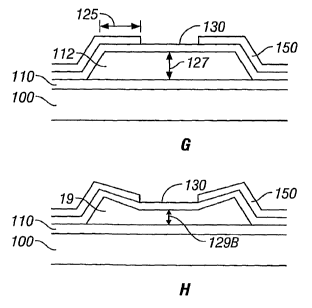
deposition of
overlying layers.
[0068] In Figure 9F, a highly reflective layer 122 is deposited over the posts
120 and the exposed portions of the sacrificial layer 112. A mechanical layer
124 is then
deposited over the highly reflective layer 122. For convenience, the highly
reflective
layer 122 and the mechanical layer 124 may be referred to and depicted in
subsequent
figures as a deformable reflective layer 130 (see Figs. 9G), whenever the
mechanical layer
124 is deposited directly over the highly reflective layer 122. In alternate
embodiments,
the deformable reflective layer 130 may comprise a single layer which has the
desired
optical and 'mechanical properties. For example, mechanical or moving layers
for
mechanical switches need not include reflective layers. Since the sacrificial
layer 112 is
still present at this stage of the process 200, the mechanical layer or
deformable reflective
layer 130 is typically not yet movable. A partially fabricated MEMS device
135, e.g. a
partially fabricated interferometric modulator, that contains a sacrificial
layer (the layer
112 in this embodiment) may be referred to herein as an "unreleased" MEMS
device.
[0069] In Figure 9G, a release etch is performed to remove the sacrificial
layer
112, forming an interferometric modulator element 140 having an
interferometric cavity
19 through which the deformable reflective layer 130 can be moved in order to
change the
color reflected by the released interferometric modulator element 140. Prior
to the release
etch, the deformable reflective layer 130 is preferably patterned to form
columns (not
shown), and may advantageously be further patterned to form etch holes (not
shown)
which facilitate access to the sacrificial layer by the release etch.
[0070] In another embodiment support structures may take the form of rivet
structures overlying the mechanical or deformable reflective layer 130. A
process for
forming overlying rivet structures is discussed and depicted with respect to
Figures l0A-
10D. In one embodiment, this process includes the steps of Figures 9A-9C. In
Figure
10A, it can be seen that a mechanical layer or deformable reflective layer 130
is deposited
over the pattemed sacrificial layer 112, such that the deformable reflective
layer 130 coats
the side walls and base of the tapered apertures 114.
[0071] In Figure IOB, a rivet layer 142 is deposited over the deformable
reflective layer 130. The rivet. layer 142 may comprise, for example, SiOz,
SiN,z, or Ni,
19
CA 02656530 2008-12-29
WO 2008/005109 PCT/US2007/011812
but a wide variety of alternate materials may be utilized for the rivet layer
142. Next, in
Figure IOC, the rivet layer is pattemed and etched to form rivet structures
150. Since the
sacrificial layer 112 is still present at this stage of the process 200, the
mechanical layer or
deformable reflective layer 130 is typically not yet movable. A partially
fabricated
MEMS device 135, e.g. a partially fabricated interferometric modulator, that
contains a
sacrificial layer (the layer 112 in this embodiment) may be referred to herein
as an
"unreleased" MEMS device. In Figure '10D, it can be seen that the sacrificial
layer 112
has been removed via a release etch, permitting the deformable reflective
layer 130 to be
able to move through the interferometric cavity 19 of the released
interferometric
modulator 140.
[0072] It will be understood that additional support may be provided through a
combination of posts 120 (Fig. 9G) and rivets 150 (Fig. lOD). For instance,
rivets 150
may be formed in some locations within an interferometric modulator, and posts
120 may
be formed at others, or rivets 150 may be formed overlying the posts 120.
[0073] = In the process described with respect to Figures 9A-9G, it can be
seen
that the sacrificial layer 112 is exposed to the etching process which
patterns the inorganic
post 120 (see Figure 9E) and the support post 120 is similarly exposed to the
release etch
which removes the sacrificial layer 112 (see Figure 9G). Unless modifications
are made
to the process flow, the support post material 118 should be selectively
etchable relative
to the sacrificial material, and vice versa. In addition even if an etch
exists which will
selectively etch one relative to another, alternate etches which are not
selective may be
preferable for other reasons.
[0074] Flexure of the support structures and the mechanical layer may occur as
a result of unbalanced stresses within the support structures and the
mechanical layer. In
some situations, these unbalanced stresses are the result of inherent stresses
within the
materials forming the support structures and the mechanical layer, which are a
function of
the materials comprising those layers. An additional source of unbalanced
stresses is the
thermal expansion of the layers, which is a function of the mismatch between
the
coefficients of thermal expansion of two different materials, the operating
temperature of
the MEMS device, the moduli of elasticity of the materials, and the material
deposition
conditions. When adjoining layers have different coefficients of thermal
expansion,
deflection may not only be caused by the relative change in size of adjoining
layers, but
the total deflection may vary as the result of the operating temperature.
Because such
CA 02656530 2008-12-29
WO 2008/005109 PCT/US2007/011812
deflection will alter the height of the interferometric cavity, and therefore
affect the color
reflected by the interferometric modulator element, it is desirable to take
this flexure into
account in manufacturing interferometric modulator elements with different
cavity
heights. In one embodiment, a single thickness sacrificial layer is applied,
rather than
multiple depositions of sacrificial material corresponding to the multiple
cavity heights,
and posts and/or rivets exhibiting differing flexures will produce multiple
cavity heights
upon release of the interferometric modulators.
[0075] Figure I 1 is a flow diagram illustrating certain steps in an
embodiment
of a method of making a device such as a MEMS device having a cavity. Such
steps may
be present in a process for manufacturing, e.g., interferometric modulators of
the general
type illustrated in Figures I and 7, along with other steps not shown in
Figure 11. Many
of the steps of the process in Figure 11 are similar to steps depicted
schematically in
Figures 9 and 10. The process of Figure 11 may be used to manufacture MEMS
devices
such as the various unreleased and released interferometric modulators
depicted in
Figures 12A through 12K. The devices shown in Figure 12 include flexure
controllers
that will produce multiple interferometric cavity heights while requiring
fewer deposition,
masking and etching steps. With reference to Figures 9, 10, 11 and 12, the
process 200
begins at step 205 where a substrate 100 is provided. In one embodiment, the
substrate
100 may comprise any transparent material such as glass or plastic.
[0076] The process 200 continues at step 210 with the formation of a first
electrically conductive layer 102 on the substrate 100 as shown in Figure 9A.
The first
electrically conductive layer 102 can be a single layer structure or multiple
sub-layer
structure as described above.
[0077] The process 200 continues at step 215 with the formation of one or
more other layers, e.g., a partially reflective layer 104, and a dielectric
layer 106 over at
least a portion of the electrically conductive layer 105 as shown in Figure
9A. The
combination of the layers 102, 104, and 106 is referred to as the optical
stack 110 as
shown in Figure 9B and Figure 12.
[0078] The process 200 continues at step 220 with the formation of a
sacrificial layer 112 as shown in Figure 9B. In Figures 9, 10 and 12A through
12H, a
single sacrificial layer is formed between the deformable reflective layer 130
(e.g.,
including both the highly reflective layer 122 and the mechanical layer 124)
and the
optical stack 110. In the interferometric modulators shown in Figure 121, 12J
and 12K, a
21
CA 02656530 2008-12-29
WO 2008/005109 PCT/US2007/011812
first sacrificial layer 1 12A is formed over the optical stack 110 prior to
the formation of a
movable reflective layer 14 (including the highly reflective layer 122) at
step 225. In the
embodiments shown in Figures 121, 12J and 12K, the movable reflective layer 14
may be
considered as a movable element that is suspended over the substrate by a
mechanical
layer 34. Without loss of generality, the term movable element will herein be
used to
describe any movable element in a MEMS device, e.g., a movable or deformable
reflective layer 130 as shown in Figures 9 and 10, any of the movable
reflective layers 14,
14a or 14b as shown in Figures 1 and 7, or the movable elements 14 as shown in
Figures
121, 12J and 12K. The movable element 14 may be formed by a deposition
followed by
patterning and etching. After forming the movable element 14, a second
sacrificial layer
112B is deposited over the movable element 14. Subsequent patternirig and
etching of the
second sacrificial layer 112B (or the single sacrificial layer 112) may
performed to form
support structure apertures 114 as shown in Figures 9C and 10A as well as
apertures for
attaching the mechanical layer 34 to the movable element 14 as shown in Figure
12. In a
preferred embodiment only one deposition is performed in forming the
sacrificial layer
112 (or 11 2A) between the movable reflective element 14 (as shown in Figure
12) or the
deformable reflective layer 130 (as shown in Figures 9 and 10) and the
substrate.
100791 In an embodiment of an interferometric modulator, the sacrificial layer
is deposited so as to form, upon subsequent removal, an interferometric cavity
with a
thickness in the range of about 1000 angstroms to about 5000 angstroms between
the
movable layer 14 or the deformable reflective layer 130 and the optical stack
16 of
Figures 1, 7 and 12.
[0080] In the dual sacrificial layer embodiments shown in Figure 121, 12J and
12K, the process 200 continues at step 230 with the formation of a mechanical
layer 34
over at least a portion of the sacrificial layer 112B and at least a portion
of the movable
element 14. In the single sacrificial layer embodiment of Figures 9 and 10,
the
mechanical layer 34"is replaced by the mechanical layer 124 that is formed
over the highly
reflective layer 122. The mechanical layers 34 and 124 may be comprised of the
same or
different materials.
[0081] The process continues at step 235 where flexure controllers are formed.
In the exemplary process 200 shown in Figure 11, a plurality of flexure
controllers having
different dimensions are formed in order to provide multiple cavity sizes
after removal of
the sacrificial layer. In another embodiment, a flexure controller is formed
to provide a
22
CA 02656530 2008-12-29
WO 2008/005109 PCT/US2007/011812
desired cavity size that is either smaller or larger than the cavity prior to
removal of the
sacrificial layer. The flexure controllers, e.g., post structures andlor rivet
structures,
induce displacement of a membrane to which the flexure controllers are
attached (e.g., the
deformable reflective layer 130), subsequent to removal of the sacrificial
layer(s) 112.
Details of some exemplary flexure controllers will be discussed below.
[0082) The process 200 continues at step 240 where the sacrificial layer 112
is
removed (e.g., by etching) to form a cavity 19 as shown in Figure lOG. The
removal of
the sacrificial layers can be accomplished, for example, by exposure to an
etchant such as
XeF2, F2 or HF alone or in combination. In a preferred embodiment,
substantially all of
the sacrificial layer 112 is removed in the etching process. In one
embodiment, the cavity
19 is an interferometric cavity between an optical stack 110 and the
deformable reflective
layer 130. After formation of the cavity 19, the resulting MEMS device, e.g.,
the
interferometric modulator, is in a `released" state.
[0083] Some examples of flexure controllers that may be formed at step 235
of the process 200 will now be discussed. For example, Figure 12A shows an
unreleased
device, e.g., an interferometric modulator, which includes posts 120 having a
wing
portion of dimension 122 substantially parallel to the substrate 100 and the
deformable
reflective layer 130. The sacrificial layer 112 has a thickness 126 as
measured
perpendicular to the substrate 100 and optical stack 110. Figure 12B shows the
device
after removal of the sacrificial layer 112 forming the cavity 19. The released
device of
Figure 12B has a cavity depth of 128A as measured perpendicular to the
substrate 100 and
optical stack 110. The depth of the cavity between the released deformable
layer 130 and
the optical stack 110 (shown as Ref. No. 128A) is measurably larger in this
example than
the unreleased cavity depth of 126 shown in Figure 12A. The difference in
cavity depth is
due to the flexure controlled by the combined stresses of the posts 120 and
the deformable
reflective layer 130.
[0084) Figure 12C shows a second example of an unreleased device, e.g., an
interferometric modulator, which includes posts 120 having a wing portion of
dimension
124 substantially parallel to the substrate 100 and the deformable reflective
layer 130. In
this example, the sacrificial layer 112 has approximately the same thickness
126 as
measured perpendicular to the substrate 100 and optical stack 110 as the
device shown in
Figure 12A. However, the overlap 124 of Figure 12C is larger than the overlap
122 of
Figure 12A. The overlaps 122 and 124 of the posts 120 are the result of
patterning and
23
CA 02656530 2008-12-29
WO 2008/005109 PCT/US2007/011812
etching steps as discussed above and shown in Figure 9E. Figure 12D shows the
device
of Figure 12C after removal of the sacrificial layer 112 forming the cavity
19. The
released device of Figure 12D has a cavity depth of 128B as measured
perpendicular to
the substrate 100 and optical stack 110. The depth of the cavity between the
released
deformable layer 130 and the optical stack 110 (shown as Ref. No. 128B) is
measurably
larger in this example than the unreleased cavity depth of 126 shown in Figure
12A and
12C and larger than the released cavity depth 128A shown in Figure 12B. The
difference
in cavity depth is due to the flexure controlled by the combined stresses of
the posts 120
(having the overlap 124 compared to the overlap 122 of Figure 12A) and the
deformable
reflective layer 130.
100851 Figures 12E and 12G show examples of a devices wherein the flexure
controllers comprise rivets 150 (as discussed above and shown in Figure 10)
overlying the
deformable reflective layer 130. The rivets 150 of Figure 12E have a smaller
overlapping
portion (or wing) than the rivets 150 of Figure 12G (see dimensions 123 and
125). In this
example, the depth 127 of the sacrificial layer 112 is approximately the same
for both
devices. However, after release of the devices, the corresponding cavity
depths may vary
significantly as depicted by the depth 129A of Figure 12F and the depth 129B
of Figure
12H.
[0086] Figures 121, 12J and 12K depict examples of unreleased
interferometric modulators with various flexure controlling post structures
120 and rivet
structures 150. Figure 121 has rivet structures 150 overlying the mechanical
layer 34 and
post structures underlying the mechanical layer 34 where the rivets 150 and
posts 120
have similar overlap. The rivet structures 150 of Figure 12J, exhibit much
less overlap
while the post structures 120 exhibit more overlap. Figure 12K depicts a
device where
the rivet structures have significantly more overlap that the post structures
120.
[0087] During fabrication of interferometric modulators, upward flexures of
movable reflective layers, upon releasing of the device (as depicted in
Figures 12B and
12D), of about 500 angstroms or less have been observed. However, downward
flexures
of movable reflective layers, upon releasing of the device (as depicted in
Figures 12F and
121), typically never occur. By varying the size and/or material of which the
flexure
controllers, e.g., posts and/or rivets, are comprised, increased upward
flexure and/or
downward flexure of inembranes may be achieved. For example, depositing
thinner post
and/or rivet layers may result in less upward flexure or increased downward
flexure.
24
CA 02656530 2008-12-29
WO 2008/005109 PCT/US2007/011812
Forming flexure controllers of more rigid materials may result in less
flexure. Decreasing
tensile stress in an overlying flexure controller, e.g., a rivet, may reduce
upward flexure.
Decreasing tensile stress in an underlying flexure controller, e.g., a post,
may increase
upward flexure. Tensile stresses tend to shrink the portion of the device in
which they are
contained. In contrast, compressive stresses tend to expand the portion of the
device in
which they are contained. One of skill in the art will recognize that by
varying the relative
sizes of posts 120 and/or rivets 150 as well as varying materials of which the
posts 120
and/or rivets 150 are comprised, significantly different released cavity
depths may be
achieved. Ranges of flexure, upward or downward, including about 50 to 100,
about 100
to 150, about 150 to 200, about 200 to 250, about 250 to 300, about 300 to
350, about 350
to 400, about 400 to 450, about 450 to 500, about 500 to 550, about 550 to
600, about 600
to 650, about 650 to 700, about 700 to 750, about 750 to 800, about 800 to
850, about 850
to 900, about 900 to 950, about 950 to 1000, about 1000 to 1050, about 1050 to
1100,
about 1100 to 1150, about 1150 to 1200 angstroms or more may be achieved by
varying
sizes and/or material properties of flexure controllers as discussed above. In
addition,
increments or decrements to these ranges of about 5, 10, 15, 20, and 25
angstroms may be
possible.
(0088] The methods described herein for controlling cavity depth of MEMS
devices may have a positive effect on the manufacture of various devices
including
MEMS devices that comprise cavities, e.g., interferometric modulators. For
example,
Table 1 summarizes the results of a set of experiments in which various post
structure
overlaps were fabricated in interferometric modulators having similar
unreleased
sacrificial layer depths. Post structure overlaps, similar to the overlaps 122
and 124
depicted in Figures 12A and 12C respectively, were varied from 1 micron to 3
microns for
interferometric modulator pixels measuring 222 microns by 222 microns. The
thickness
of the sacrificial layer in these experiments was about 1150 angstroms. After
releasing
the interferometric modulators, the undriven cavity depth (as measured
perpendicular to
the substrate) between the movable element and the optical stack varied
significantly.
CA 02656530 2008-12-29
WO 2008/005109 PCT/US2007/011812
Table I
Post Overlap ( m) Undriven Cavity Depth
(Angstroms)
1.0 1400
2.0 1775
2.5 2000
3.0 2200
[0089] Relatively small changes in post overlap resulted in more than 50%
variation in undriven cavity depth from the shallowest to the deepest cases
shown in
Table 1. By varying dimensions and or materials of posts and/or rivets as
discussed
above, even larger variations may be demonstrated. The post structures used in
the test
resulted in increases in gap size due to the tensile stress in the post
structures (See Figure
12B and 12D). However, by utilizing rivet structures and/or combinations of
post and
rivet structures, decreases or sagging of the deformable reflective layer (as
depicted in
Figures 12F and 12H) may also be realized. As discussed above, cavity depths
of about
1000 angstroms to about 5000 angstroms are desirable for interferometric
modulators. A
range of cavity sizes from about 2000 angstroms to about 4000 angstroms is
preferred for
modulating visible light while smaller and/or larger cavity sizes may be used
for
modulating hyperspectral light, ultraviolet light and/or infrared light.
Increases in cavity
depth of about 30% to 40%, about 40% to 50%, about 50% to 60%, about 60% to
70%,
about 70% to 80%, about 80% to 90%, about 90% to 100% or more may be achieved.
In
addition, increments or decrements to these ranges of about 1%, 2%, 3%, 4% and
5% may
be obtained.
[0090] In addition to the experiments discussed above that have shown the
effect that various structures of flexure controllers have on cavity depth,
analytical studies
have also been made that simulate the experiments and indicate that additional
capability
of controlling the cavity depth may also be afforded. Figures 13A-13F show
results of
analytical studies designed to show the effects that altering the
characteristics of flexure
controller structures can have on a deflection of a supported layer upon
release of the
device. The analytical equations used in the studies model the effects of
stresses, both
26
CA 02656530 2008-12-29
WO 2008/005109 PCT/US2007/011812
tensile and compressive, contained in the various rivets and/or post
structures when
combined with the stresses contained in a layer that they are supporting. The
modeled
stresses contained in the support structures and in the supported layer
represent stresses
that may result depending on the conditions under which the different layers
are formed.
Compressive stresses, designated by negative stress levels in the studies,
tend to expand
the portion of the device in which they are contained. Tensile stresses,
designated by
positive stress levels in the studies, tend to shrink the portion of the
device in which they
are contained. The studies looked at various combinations of posts and/or
rivet structures.
The studies also modeled the effect that ranges of certain dimensions and/or
characteristics of different portions of the flexure controller structures
have on the
resulting deflection. The dimensions and characteristics of the flexure
controller
structures that were analyzed include layer thickness, overlap length, and
stress level of
the various portions of the device. The analysis modeled the flexure
controller posts
and/or rivets and the supported layer as cantilevered beams. The structures
used in the
analysis are representative of any of several types of devices including, but
not limited to,
MEMS devices, light modulating devices, and any device comprising one or more
thin
film layers having a cavity between one of the thin film layers and the
substrate and/or
between two of the thin film layers.
[0091] The results shown in Figures 13A-13F will be discussed in relation to
the interferometric modulator embodiments shown in Figure 12. It should be
noted that
the interferometric modulator is an example of a device that may be modeled
using the
analytical methods presented here, and other devices may also be analyzed and
manufactured using the various methods described above.
[0092] The configuration of the device analyzed in the first example includes
a
1000 angstrom thick (as measured perpendicular to the substrate 100)
deformable
reflective layer 130 comprised of Ni. The Ni layer is modeled with a 400 MPa
tensile
stress that is representative of the type of stress levels seen under typical
deposition
conditions. The device also includes a 2000 angstrom thick (as measured
perpendicular to
the substrate) oxide post structure 120. The oxide post structures modeled in
the analysis
comprised Si02. The post structure overlaps the deformable reflective layer
130 by 3 m,
where the overlap is measured as depicted by the dimensions 122 and 124 shown
in
Figures 12A and 12C. The post structure is modeled with a-400 -MPa compressive
stress.
The device also includes an oxide rivet structure 150, where the thickness of
the rivet
27
CA 02656530 2008-12-29
WO 2008/005109 PCT/US2007/011812
structure (as measured perpendicular to the substrate) is 1000 angstroms for
Figure 13A
and is variable on the horizontal axis for Figure 13B. The rivet structure
overlaps the
deformable reflective layer 130 by 3 m, where the overlap is measured as
depicted by the
dimensions 123 and 125 shown in Figures 12E and 12G. The stress of the rivet
structure
is variable on the horizontal axis for the analysis results shown in Figure
13B and is -400
MPa for the analysis results shown in Figure 13B. Figures 13A and 13B show the
resulting deflections, upon release of the sacrificial layer 112 resulting in
the cavity 19, of
the deformable reflective layer 130. Positive deflection values represent
deflections away
from the substrate 100 as depicted in Figures 12B and 12D. Negative deflection
values
represent deflection towards the substrate 100 as depicted in Figures 12F and
12H.
100931 The results of Figure 13A show that for increased compressive stress
(more negative values), the deflection is lower, showing an estimated
deflection of just
over 300 angstroms for a -500 MPa oxide rivet stress. As the compressive
stress is
reduced to zero, the deflections become larger, showing an estimated
deflection greater
than 800 angstroms for a zero MPa stress level. Deflections of even greater
values can be
obtained by forming rivet structures with tensile stress levels (positive
stress). The reason
that all the deflections are positive (away from the substrate) in the example
of Figure
13A is that the combined oxide post stress of -400 MPa and the deformable
reflective
layer stress of 400 MPa both contribute to a positive deflection that the
oxide rivet stress
levels analyzed do not overcome. Smaller values of deflection, including
negative
deflection values, could be obtained by several methods, including applying
more
negative compressive rivet stress levels, reducing the thickness of the
compressed oxide
post, reducing the compressive stress of the oxide post, reducing the
thickness of the
compressed oxide post, increasing the thickness of the compressed oxide rivet,
reducing
the overlap length of the compressed oxide post, increasing the overlap length
of the
compressed rivet and other methods known to those of skill in the art. These
methods all
serve to reduce the energy levels of portions of the device contributing to
upward
deflections (e.g., the compressed post 120 and the stretched deformable
reflective layer
130) and/or increase the energy levels of portions of the device contributing
to downward
deflections (e.g., the compressed rivet 150).
[0094) The results of Figure 13B show that as the thickness of the compressed
oxide rivet 150 is increased (increasing the energy contributing to a downward
28
CA 02656530 2008-12-29
WO 2008/005109 PCT/US2007/011812
deflection), the deflection, upon release of the sacrificial layer 112, is
reduce, even
becoming a negative value for rivet thicknesses greater than about 2000
angstroms.
[0095] The next example includes a 2000 angstrom thick oxide post 120 with
a compressive stress of -400 MPa, a 1000 angstrom thick oxide rivet 150 with a
compressive stress of -400 MPa, and a 1000 angstrom thick deformable
reflective Ni layer
130 with a tensile stress of 400 MPa. The overlap lengths of the post 120 (see
the
dimensions 122 and 124 in Figures 12A and 12C) and the rivet 150 (see the
dimensions
123 and 125 in Figures 12E and 12G) are equal and are varied from about 2 m
to about
6 m. Figure 13C shows the estimated deflections of the deformable reflective
layer 130
upon release of the sacrificial layer 112: Increasing the overlap lengths of
both the post
120 and the rivet 150 increases deflections away from the substrate 100. As in
the cases
above, the compressed post 120 and the stretched deformable reflective layer
130 both
contribute to the upward deflections and the compressed rivet 150 contributes
to a
downward deflection. In this case, the combined energies of the layer 130 and
the post
120 outweigh the energy of the rivet 150 and the deflections are all positive.
By varying
the overlap lengths of the oxide post 120 and the oxide rivet 150 from about 2
m to
about 6 m, the deflection of the layer 130 can be varied from about 200
angstroms to
abut 1700 angstroms.
[00961 Figure 13D shows deflections of the deformable reflective layer 130,
upon release of the sacrificial layer 112, for a case similar to that of
Figure 13C except
that there is no oxide rivet. In this example, the positive deflections of the
deformable
reflective layer 130 are even greater than without the rivet because the
compressed rivet is
not working against the upward deflections caused by the post 120 and the
deformable
reflective layer 130. By varying the overlap length of the oxide post 120 from
about 2 m
to about 6 m, the deflection of the layer 130 can be varied from about 500
angstroms to
abut 5500 angstroms.
[00971 Figure 13E shows deflections of the deformable reflective layer 130,
upon release of the sacrificial layer 112, for a case similar to that of
Figure 13D (including
no oxide rivet) but with a fixed oxide post 120 overlap of 3 m (see
dimensions 122 and
124 in Figures 12A and 12C) and varied oxide post stress levels. In this
example, the
positive deflections of the deformable reflective layer 130 decrease for less
negative
values (lower compressive stress levels) of oxide post stress. For a
compressive oxide
post stress level of 500 MPa, the upward deflection of the deformable
reflective layer 130,
29
CA 02656530 2008-12-29
WO 2008/005109 PCT/US2007/011812
upon release of the sacrificial layer 112, is about 1600 angstroms, and is
about 350
angstroms for a zero stress level.
[00981 The final example includes a 2000 angstrom thick oxide post 120 with
a compressive stress of -400 MPa, a 1000 angstrom thick oxide rivet 150 with a
compressive stress of -200 MPa, and a 1000 angstrom thick deformable
reflective Ni layer
130 with a tensile stress of 400 MPa. The overlap lengths of the post 120 (see
the
dimensions 122 and 124 in Figures 12A and 12C) and the rivet 150 (see the
dimensions
123 and 125 in Figures 12E and 12G) are equal and are varied from about 2 m
to about
6 m. Figure 13F shows the estimated deflections of the deformable reflective
layer 130
upon release of the sacrificial layer 112. Increasing the overlap lengths of
both the post
120 and the rivet 150 increases deflections away from the substrate 100. As in
the cases
above, the compressed post 120 and the stretched deformable reflective layer
130 both
contribute to the upward deflections and the compressed rivet 150 contributes
to a
downward deflection. In this case, the combined stress levels of the layer 130
and the
post 120 outweigh the stress level of the rivet 150 and the deflections are
all positive. By
varying the overlap lengths of the oxide post 120 and the oxide rivet 150 from
about 2 m
to about 6 m, the estimated deflection of the layer 130 varies from about 250
angstroms
to abut 2500 angstroms.
[00991 The analytical studies of the examples discussed above show that
variation in dimensions and/or characteristics of the various portions making
up the
flexure controller structures and/or other layers can affect the deflection of
a supported
layer upon release of the device. Those of skill in the art will be able to
recognize other
ways of modifying portions of similar types of devices in order to alter the
cavity depth of
the released device.
[0100] An embodiment of an unreleased interferometric modulator includes
first means for reflecting light, second means for rzflecting light, first
means for
supporting the second reflecting means, wherein the first supporting means is
removable
by etching, and second means for supporting the second reflecting means and
for forming
a cavity between the first reflecting means and the second rellecting means,
upon removal
of the first supporting means, of a depth about 30 percent greater or more
than the depth
of the first supporting means, wherein depth is measured perpendicular to the
first
reflecting means. With reference to Figures 9 and 12, aspects of this
embodiment include
where the first reflecting means is a partially reflective layer 104, where
the second
CA 02656530 2008-12-29
WO 2008/005109 PCT/US2007/011812
reflecting means is a movable reflective layer 14, where the first supporting
means is a
sacrificial layer 112, and where the second supporting means is at least one
of a post
structure 120 and a rivet structure 150.
101011 Another embodiment of an unreleased interferometric modulator
includes first means for reflecting light, second means for reflecting light,
first means for
supporting the second reflecting means, and second means for supporting the
second
reflecting means and for effecting a displacement of the second reflecting
means towards
the first reflecting means upon removal of the first supporting means, wherein
the first
supporting means is removable by etching. With reference to Figures 9 and 12,
aspects of
this embodiment include where the first reflecting means is a partially
reflective layer
104, where the second reflecting means is a movable reflective layer 14, where
the first
supporting means is a sacrificial layer 112, and where the second supporting
means is at
least one of a post structure 120 and a rivet structure 150.
[0102] While the above detailed description has shown, described, and pointed
out novel features of the invention as applied to various embodiments, it will
be
understood that various omissions, substitutions, and changes in the form and
details of
the device or process illustrated may be made by those skilled in the art
without departing
from the spirit of the invention. As will be recognized, the present invention
may be
embodied within a form that does not provide all of the features and benefits
set forth
herein, as some features may be used or practiced separately from others.
31