Note: Descriptions are shown in the official language in which they were submitted.
CA 02656686 2008-12-30
SPECIFICATION
MICRO PASSAGE CHIP AND FLUID TRANSFERRING METHOD
TECHNICAL FIELD
[0001] The present invention relates to a micro passage chip that is
extensively
used in chemical/biochemical analyses such as gene analysis. More
particularly,
the present invention relates to a micro passage chip having a simple fluid
transfer mechanism for transferring samples of fluids such as liquids or
gases.
BACKGROUND ART
[0002] Devices commonly known as "micro-total analysis systems ( TAS)" or
"lab-on-chip" comprise a substrate and microstructures such as micro-channels
and ports that are provided in the substrate to form channels of specified
shapes.
It has recently been proposed that a variety of operations such as chemical
reaction, synthesis, purification, extraction, generation and/or analysis be
performed on substances in the microstructures, and some of the proposals have
been commercialized. Structures that are fabricated for this purpose and which
have microstructures such as micro-channels and ports provided in the
substrate
are collectively referred to as "micro-fluid devices" or "micro-channel
chips".
[0003] Micro-channel chips find use not only in chemical, biochemical,
pharmaceutical, medical and veterinary fields for gene analysis, clinical
diagnosis, drug screening and the like but also in a wide range of
applications
including chemical engineering and environmental monitoring. Compared to
devices of the same type in usual size, micro-channel chips have various
advantages including (1) extremely smaller amounts of samples and reagents
that need to be used, (2) shorter analysis time, (3) higher sensitivity, (4)
portability to the site for on-site analysis, and (5) one-way use.
- 1 -
CA 02656686 2008-12-30
[0004] A conventional micro-channel chip is shown in FIGS. 10A and lOB, where
it is indicated by numeral 100. As shown, the micro-channel chip 100 comprises
an upper substrate 102 that is formed of a material such as a synthetic resin,
at
least one micro-channel 104 formed in the upper substrate 102, ports 105 and
106 formed in at least one end of the micro-channel 104 to serve as an input
port
and an output port, and a lower substrate 108 that is adhered to the lower
side of
the substrate 102 and which is formed of a transparent or opaque material (for
example, glass or a synthetic resin film). The lower substrate 108 helps seal
the
bottoms of the ports 105 and 106, as well as the micro-channel 104. The
materials and structures of micro-channel chips of the type shown in FIGS. 10A
and lOB, as well as processes for producing them may be found in Patent
Documents 1 and 2.
[0005] The micro-channels in the micro-channel chip, in order to transfer a
fluid
(mainly a liquid or gas such as a liquid chemical or sample) from one area to
another, occasionally employs a physical or mechanical squeezing means that is
applied from the outer surface of the substrate. For example, Patent Document
3 describes a fluid processing device comprising (a) a substrate fixing
platform
for fixing a substrate formed of an elastic polymeric material having a micro-
channel formed in the interior, (b) a solid structure as a pressurizing means
that
applies pressure from the outside to a surface of the substrate, (c) a linear
moving unit as a moving means that is linked to the solid structure or the
substrate fixing platform and which moves such solid structure or substrate
fixing platform in the longitudinal direction of the micro-channel, and (d) a
section that descends the solid structure vertical to the substrate in order
to
apply pressure to the substrate.
[0006] In addition, Patent Document 4 describes a cartridge for biochips that
comprises (a) a flat plate of substrate member that is formed of an elastic
material and (b) a flexible cover of harder material than the substrate member
that is mounted in contact with both the upper and lower surfaces of the
- 2 -
CA 02656686 2008-12-30
substrate member, the substrate member having a sampling section for
collecting a biopolymer and a pretreatment section that performs a
pretreatment
on the biopolymer; according to Patent Document 4, the cover is pressed down
by
a roll of rigid body for progressively moving the biopolymer from the sampling
section toward the pretreatment section.
[0007] Furthermore, Patent Document 5 describes a micro-reactor of sheet type
in the form of an assembly of flexible sheets that are superposed in intimate
contact, which has in its interior (a) a first void section for holding an
analyte, (b)
a plurality of second void sections communicating with the first void section,
and
(c) a third void section that communicates with the second void sections and
which holds a reagent to perform a chemical reaction with the analyte, further
characterized in that a fixed member that serves as a shaft for causing
rotation
along the surface of the sheet assembly is provided on that surface of the
side
where the third void section is provided.
[0008] Further in addition, Patent Document 6 describes a cartridge for
chemical
reactions that comprises a vessel at least part of which is formed of an
elastic
material, the vessel having formed in it a plurality of compartments that are
connected or arranged connectable by channels, further characterized in that
by
applying an external force to the elastic material from the outside of the
vessel, a
material either in the channel(s) or the compartment(s) or in both is moved to
perform a chemical reaction, wherein either the channel(s) or the
compartment(s) or both have a capacity of zero before the fluid material is
flowed
in. In the case of this cartridge, if the fluid material is flowed into the
channel(s)
and compartment(s), a roller is rolled over the cartridge so as to depress its
outer
surface, whereby the fluid material is moved in a specified direction.
[0009] The problem with the device of Patent Document 3 is that it is
extremely
difficult to maintain the positional precision while applying a mechanical
pressure to the concave channel and no fluid transfer is possible if a
positional
mismatch occurs. The devices of Patent Documents 4 to 6 are effective for
large
- 3 -
CA 02656686 2008-12-30
spaces or channel structures of a simple orientation but they are incapable of
complicated squeezing actions such as introducing a liquid chemical through
four
adjacent ports into the same reaction vessel at different times, or agitating
the
liquid chemical by reciprocating it at millisecond intervals, or transferring
the
liquid chemical from one channel to an adjacent channel that is apart by only
a
few millimeters. In addition, being a mechanical pressurizing means or a
transfer means involving centrifugal force, those devices require a moving
part,
which makes it difficult to sufficiently reduce their size (that they become
portable). As a further problem, the physical or mechanical squeezing means is
slid over the substrate as it is depressed against the substrate's outer
surface, so
the substrate is often damaged making it necessary to perform another
analysis.
Patent Document 1: Official gazette of JP 2000-27813 A
Patent Document 2: Official gazette of JP 2001-157855 A
Patent Document 3: Specification of Japanese Patent No. 3732159
Patent Document 4: Specification of Japanese Patent No. 3865134
Patent Document 5: Specification of Japanese Patent No. 3746207
Patent Document 6: Official gazette of JP 2005-313065 A
DISCLOSURE OF THE INVENTION
PROBLEMS TO BE SOLVED BY THE INVENTION
[0010] Therefore, an object of the present invention is to provide a novel
micro
passage chip having such a structure that a fluid can be transferred without
using a physical or mechanical squeezing means that is applied from above the
substrate of the micro passage chip.
[0011] Another object of the present invention is to provide a novel fluid
transferring method using this micro passage chip.
- 4 -
CA 02656686 2008-12-30
MEANS FOR SOLVING THE PROBLEMS
[0012] As one means for attaining the first-stated object, the invention
according
to claim 1 provides a micro passage chip comprising at least a first
substrate, a
second substrate, and an intermediate substrate interposed between the first
substrate and the second substrate, wherein
a first non-adhesive thin-film layer is formed on at least one of the mating
sides of the first substrate and the intermediate substrate and at least one
port
for fluids that is in contact with the first non-adhesive thin-film layer and
which
is open to the outer surface of the first substrate is provided in any
position on
the first non-adhesive thin-film layer, and
at least a portion of a second non-adhesive thin-film layer whose length is
either the same as or different from that of the first non-adhesive thin-film
layer
is formed on at least one of the mating sides of the second substrate and the
intermediate substrate such that it lies either above or under the first non-
adhesive thin-film layer, with the intermediate substrate lying in between,
and a
pressurizing port that is in contact with the second non-adhesive thin-film
layer
and which is open to the outer surface of the first or the second substrate is
provided in at least one area on the second non-adhesive thin-film layer.
[0013] According to this invention, the first substrate in the non-adhesive
part
corresponding to the first non-adhesive thin-film layer is first pressurized
so that
it inflates to create a gap into which a fluid is introduced and,
subsequently, the
intermediate substrate in the non-adhesive part corresponding to the second
non-adhesive thin-film layer is caused to inflate, whereupon the fluid within
the
gap in the first substrate is squeezed by the inflating portion of the
intermediate
substrate to enable its transfer. Thus, by forming a simple three-layered
structure, a squeezing action can be effected from within the chip. Since this
eliminates the need to bring a physical or mechanical squeezing means into
contact with the outer surface of the first substrate and to move it as it is
pressed
- 5 -
CA 02656686 2008-12-30
down, the fluid can be transferred without damaging the first substrate.
Furthermore, with no physical or mechanical squeezing means being used, the
whole size of the micro-channel chip device can be sufficiently reduced to
make it
portable.
[0014] As another means for attaining the first-stated object, the invention
according to claim 2 provides a micro passage chip which is the same as
recited
in claim 1, provided that:
a first non-adhesive part is present in the area of the interface between
the first substrate and the intermediate substrate where the first non-
adhesive
thin-film layer is formed;
a second non-adhesive part is present in the area of the interface between
the second substrate and the intermediate substrate where the second non-
adhesive thin-film layer is formed;
the first non-adhesive part serves as a channel for the fluid; and
the second non-adhesive part serves as a squeezing means for transferring
the fluid.
[0015] According to this invention, the presence of the non-adhesive part in
the
area where each of the non-adhesive thin-film layers is formed enables
inflation
by pressurization, allowing the fluid to be injected and transferred by
squeezing.
[0016] As yet another means for attaining the first-stated object, the
invention
according to claim 3 provides a micro-channel chip which is the same as
recited
in claim 1, provided that the first non-adhesive thin-film layer includes,
halfway
down it, at least one enlarged region layer having at least one planar shape
selected from the group consisting of a circular, an elliptical, a
rectangular, and a
polygonal shape.
[0017] According to this invention, the enlarged region layer in the first non-
adhesive thin-film layer can function as a liquid reservoir or a reaction
chamber,
which can be utilized to perform PCR amplification and various other chemical,
biochemical or physiological reactions. Therefore, by providing the first non-
- 6 -
CA 02656686 2008-12-30
adhesive thin-film layer with at least one enlarged region layer, the scope of
utilization of the micro-channel chip can be expanded.
[0018] As still another means for attaining the first-stated object, the
invention
according to claim 4 provides a micro passage chip which is the same as
recited
in any one of claims 1 to 3, provided that the first non-adhesive thin-film
layer
and the second non-adhesive thin-film layer each have a film thickness in the
range of 10 nm to 300 m and a width in the range of 10 m to 3000 m.
[0019] According to this invention, each of the non-adhesive thin-film layers
is
specified to have film thicknesses and widths that are suitable for transfer
by
squeezing in the micro-channel chip of the present invention.
[0020] As a further means for attaining the first-stated object, the invention
according to claim 5 provides a micro passage chip comprising at least a first
substrate, a second substrate, and an intermediate substrate interposed
between
the first substrate and the second substrate, wherein
a hollow, concave channel through which to pass a fluid is formed on the
side of the first substrate that is adhered to the intermediate substrate and
at
least one port for fluids that communicates with the concave channel and which
is open to the outer surface of the first substrate is provided at any
position in
the concave channel, and
at least a portion of a second non-adhesive thin-film layer whose length is
either the same as or different from that of the concave channel is formed on
at
least one of the mating sides of the second substrate and the intermediate
substrate such that it lies either above or under the concave channel, with
the
intermediate substrate lying in between, and a pressurizing port that is in
contact with the second non-adhesive thin-film layer and which is open to the
outer surface of the first or second substrate is provided in at least one
area on
the second non-adhesive thin-film layer.
[0021] According to this invention, there is provided a micro-channel chip in
which a substrate having a concave channel that is formed by the prior art and
- 7 -
CA 02656686 2008-12-30
which should serve as a fluid channel is combined with the transfer-by-squeeze
means of the present invention. In addition, the fluid within the concave
channel can be transferred positively without applying a physical or
mechanical
squeezing means from the outer surface of the first substrate and, what is
more,
the risk of damaging the first substrate can be eliminated.
[0022] As another means for attaining the first-stated object, the invention
according to claim 6 provides a micro passage chip which is the same as
recited
in claim 5, provided that:
a second non-adhesive part is present in the area of the interface between
the second substrate and the intermediate substrate where the second non-
adhesive thin-film layer is formed; and
the second non-adhesive part serves as a squeezing means for transferring
the fluid.
[0023] According to this invention, the second non-adhesive part is present in
the
area where the second non-adhesive thin-film layer is formed, so by inflating
the
intermediate substrate in this second non-adhesive part, the fluid within the
overlying concave channel can be transferred by squeezing.
[0024] As still another means for attaining the first-stated object, the
invention
according to claim 7 provides a micro passage chip which is the same as
recited
in claim 5 or 6, provided that the second non-adhesive thin-film layer has a
film
thickness in the range of 10 nm to 300 m and a width in the range of 10 m to
3000 m.
[0025] According to this invention, the second non-adhesive thin-film layer is
specified to have film thicknesses and widths that are suitable for transfer
by
squeezing in the micro-channel chip having the concave channel.
[0026] As yet another means for attaining the first-stated object, the
invention
according to claim 8 provides a micro passage chip comprising at least a first
substrate, a second substrate, and a first and a second intermediate substrate
- 8 -
CA 02656686 2008-12-30
that are interposed between the first substrate and the second substrate,
wherein
a first non-adhesive thin-film layer is formed on at least one of the mating
sides of the first and the second intermediate substrate and at least one port
for
fluids that is in contact with the first non-adhesive thin-film layer and
which is
open to the outer surface of the first substrate is provided in any position
on the
first non-adhesive thin-film layer,
at least a portion of a second non-adhesive thin-film layer whose length is
either the same as or different from that of the first non-adhesive thin-film
layer
is formed on at least one of the mating sides of the second substrate and the
second intermediate substrate such that it lies either above or under the
first
non-adhesive thin-film layer, with the second intermediate substrate lying in
between, and a first pressurizing port that is in contact with the second non-
adhesive thin-film layer and which is open to the outer surface of the first
or the
second substrate is provided in at least one area on the second non-adhesive
thin-film layer, and
at least a portion of a third non-adhesive thin-film layer whose length is
either the same as or different from that of the first non-adhesive thin-film
layer
is formed on at least one of the mating sides of the first substrate and the
first
intermediate substrate such that it lies either above or under the first non-
adhesive thin-film layer, with the first intermediate substrate lying in
between,
and a second pressurizing port that is in contact with the third non-adhesive
thin-film layer and which is open to the outer surface of the first or the
second
substrate is provided in at least one area on the third non-adhesive thin-film
layer.
[0027] According to this invention, a plurality of intermediate substrates are
interposed and this enables the fluid to be transferred by squeezing in
complicated ways, such as advancing, retracting, or stopping it.
- 9 -
CA 02656686 2008-12-30
[0028] As another means for attaining the first-stated object, the invention
according to claim 9 provides a micro passage chip which is the same as
recited
in claim 8, provided that:
a first non-adhesive part is present in the area of the interface between
the first and the second intermediate substrate where the first non-adhesive
thin-film layer is formed;
a second non-adhesive part is present in the area of the interface between
the second substrate and the second intermediate substrate where the second
non-adhesive thin-film layer is formed;
a third non-adhesive part is present in the area of the interface between
the first substrate and the first intermediate substrate where the third non-
adhesive thin-film layer is formed;
the first non-adhesive part serves as a channel for the fluid; and
the second and third non-adhesive parts serve as squeezing means for
transferring the fluid.
[0029] According to this invention, the presence of the non-adhesive part in
each
of the areas where the respective non-adhesive thin-film layers are formed
enables inflation by pressurization in complicated repertoire, allowing
transfer
by squeezing in various patterns.
[0030] As yet another means for attaining the first-stated object, the
invention
according to claim 10 provides a micro passage chip which is the same as
recited
in claim 8, provided that the first non-adhesive thin-film layer includes,
halfway
down it, at least one enlarged region layer having at least one planar shape
selected from the group consisting of a circular, an elliptical, a
rectangular, and a
polygonal shape.
[0031] According to this invention, the enlarged region layer can function as
a
liquid reservoir or a reaction chamber, which can be utilized to perform PCR
amplification and various other chemical, biochemical or physiological
reactions.
Therefore, by providing the first non-adhesive thin-film layer with at least
one
- 10 -
CA 02656686 2008-12-30
enlarged region layer, the scope of utilization of the micro-channel chip can
be
expanded.
[0032] As still another means for attaining the first-stated object, the
invention
according to claim 11 provides a micro passage chip which is the same as
recited
in any one of claims 8 to 10, provided that the first non-adhesive thin-film
layer,
the second non-adhesive thin-film layer, and the third non-adhesive thin-film
layer each have a film thickness in the range of 10 nm to 300 m and a width
in
the range of 10 m to 3000 m.
[0033] According to this invention, each of the three non-adhesive thin-film
layers is specified to have film thicknesses and widths that are suitable for
transfer by squeezing in the micro-channel chip of the present invention.
[0034] As yet another means for attaining the first-stated object, the
invention
according to claim 12 provides a micro passage chip which is the same as
recited
in any one of claims 1 to 11, provided that the first substrate is made of
polydimethylsiloxane (PDMS), the second substrate is made of
polydimethylsiloxane (PDMS) or glass, and the intermediate substrate(s)
is(are)
made of polydimethylsiloxane (PDMS).
[0035] According to this invention, PDMS bonds permanently to itself or to
glass,
so only those areas that correspond to the parts where the non-adhesive thin-
film layers are formed can be left as non-adhesive parts while the other parts
are
permanently bonded.
[0036] As one means for attaining the second-stated object, the invention
according to claim 13 provides a method of fluid transfer in a micro passage
chip
comprising at least a first substrate, a second substrate, and an intermediate
substrate interposed between the first substrate and the second substrate,
wherein
a first non-adhesive thin-film layer is formed on at least one of the mating
sides of the first substrate and the intermediate substrate and at least one
port
for fluids that is in contact with the first non-adhesive thin-film layer and
which
- 11 -
CA 02656686 2008-12-30
is open to the outer surface of the first substrate is provided in any
position on
the first non-adhesive thin-film layer,
at least a portion of a second non-adhesive thin-film layer whose length is
either the same as or different from that of the first non-adhesive thin-film
layer
is formed on at least one of the mating sides of the second substrate and the
intermediate substrate such that it lies either above or under the first non-
adhesive thin-film layer, with the intermediate substrate lying in between,
and a
pressurizing port that is in contact with the second non-adhesive thin-film
layer
and which is open to the outer surface of the first or the second substrate is
provided in at least one area on the second non-adhesive thin-film layer,
a first non-adhesive part is present in the area of the interface between
the first substrate and the intermediate substrate where the first non-
adhesive
thin-film layer is formed, and
a second non-adhesive part is present in the area of the interface between
the second substrate and the intermediate substrate where the second non-
adhesive thin-film layer is formed, further characterized by comprising:
(a) the step of injecting a fluid of interest under pressure through the port
so
that the first substrate in the first non-adhesive part that corresponds to
the first non-adhesive thin-film layer is inflated to create a gap and
introducing the fluid into that gap;
(b) the step of inflating, with pressure being applied through the
pressurizing
port, the intermediate substrate in the second non-adhesive part that
corresponds to the second non-adhesive thin-film layer; and
(c) the step of applying further pressure so that the gap created in the
second
non-adhesive part grows further, whereby the fluid within the gap created
in the first non-adhesive part is squeezed by the gap created in the second
non-adhesive part so that it is transferred to a desired area.
[0037] According to this invention, a squeezing action can be effected within
the
chip. Since this eliminates the need to bring a physical or mechanical
squeezing
- 12 -
CA 02656686 2008-12-30
means into contact with the outer surface of the first substrate and to move
it as
it is pressed down, the fluid can be transferred without damaging the first
substrate.
[0038] As a further means for attaining the second-stated object, the
invention
according to claim 14 provides a method of fluid transfer in a micro passage
chip
comprising at least a first substrate, a second substrate, and an intermediate
substrate interposed between the first substrate and the second substrate,
wherein
a hollow, concave channel through which to pass a fluid is formed on the
side of the first substrate that is adhered to the intermediate substrate and
at
least one port for fluids that communicates with the concave channel and which
is open to the outer surface of the first substrate is provided at any
position in
the concave channel,
at least a portion of a second non-adhesive thin-film layer whose length is
either the same as or different from that of the concave channel is formed on
at
least one of the mating sides of the second substrate and the intermediate
substrate such that it lies either above or under the concave channel, with
the
intermediate substrate lying in between, and a pressurizing port that is in
contact with the second non-adhesive thin-film layer and which is open to the
outer surface of the first or second substrate is provided in at least one
area on
the second non-adhesive thin-film layer, and
a second non-adhesive part is present in the area of the interface between
the second substrate and the intermediate substrate where the second non-
adhesive thin-film layer is formed, further characterized by comprising*
(a) the step of injecting a fluid of interest through the port that
communicates
with the concave channel so that it is introduced into the concave channel;
(b) the step of inflating, with pressure being applied through the
pressurizing
port in contact with the second non-adhesive thin-film layer, the
- 13 -
CA 02656686 2008-12-30
intermediate substrate in the second non-adhesive part that corresponds
to the second non-adhesive thin-film layer; and
(c) further inflating the intermediate substrate in the second non-adhesive
part that corresponds to the second non-adhesive thin-film layer so that it
gets into the groove of the concave channel, whereby the fluid within the
concave channel is transferred in a specified direction.
[0039] According to this invention, even a substrate having a concave channel
that is formed by the prior art and which should serve as a fluid channel
enables
fluid transfer if it is combined with the transfer-by-squeeze means of the
present
invention.
[0040] As yet another means for attaining the second-stated object, the
invention
according to claim 15 provides a method of fluid transfer in a micro passage
chip
comprising at least a first substrate, a second substrate, and a first and a
second
intermediate substrate that are interposed between the first substrate and the
second substrate, wherein
a first non-adhesive thin-film layer is formed on at least one of the mating
sides of the first and the second intermediate substrate and at least one port
for
fluids that is in contact with the first non-adhesive thin-film layer and
which is
open to the outer surface of the first substrate is provided in any position
on the
first non-adhesive thin-film layer,
at least a portion of a second non-adhesive thin-film layer whose length is
either the same as or different from that of the first non-adhesive thin-film
layer
is formed on at least one of the mating sides of the second substrate and the
second intermediate substrate such that it lies either above or under the
first
non-adhesive thin-film layer, with the second intermediate substrate lying in
between, and a first pressurizing port that is in contact with the second non-
adhesive thin-film layer and which is open to the outer surface of the first
or the
second substrate is provided in at least one area on the second non-adhesive
thin-film layer,
- 14 -
CA 02656686 2008-12-30
at least a portion of a third non-adhesive thin-film layer whose length is
either the same as or different from that of the first non-adhesive thin-film
layer
is formed on at least one of the mating sides of the first substrate and the
first
intermediate substrate such that it lies either above or under the first non-
adhesive thin-film layer, with the first intermediate substrate lying in
between,
and a second pressurizing port that is in contact with the third non-adhesive
thin-film layer and which is open to the outer surface of the first or the
second
substrate is provided in at least one area on the third non-adhesive thin-film
layer,
a first non-adhesive part is present in the area of the interface between
the first and the second intermediate substrate where the first non-adhesive
thin-film layer is formed,
a second non-adhesive part is present in the area of the interface between
the second substrate and the second intermediate substrate where the second
non-adhesive thin-film layer is formed, and
a third non-adhesive part is present in the area of the interface between
the first substrate and the first intermediate substrate where the third non-
adhesive thin-film layer is formed, further characterized by comprising*
(a) the step of injecting a fluid of interest under pressure through the port
so
that the first substrate in the first non-adhesive part that corresponds to
the first non-adhesive thin-film layer is inflated to create a gap and
introducing the fluid into that gap;
(b) the step of inflating, with pressure being applied through the first
pressurizing port, the second intermediate substrate in the second non-
adhesive part that corresponds to the second non-adhesive thin-film layer
and/or inflating, with pressure being applied through the second
pressurizing port, the first intermediate substrate in the third non-
adhesive part that corresponds to the third non-adhesive thin-film layer;
and
- 15 -
CA 02656686 2008-12-30
(c) the step of further growing the gap created in the second non-adhesive
part
and/or further growing the gap created in the third non-adhesive part, whereby
the fluid within the gap created in the first non-adhesive part is squeezed by
the
gap created in the second non-adhesive part and/or by the gap created in the
third non-adhesive part so that it is transferred to a desired area.
[0041] According to this invention, a plurality of intermediate substrates are
interposed and this enables the fluid to be transferred by squeezing in
complicated ways, such as advancing, retracting, or stopping it.
EFFECTS OF THE INVENTION
[0042] According to the micro passage chip and fluid transferring method of
the
present invention, the conventional physical or mechanical squeezing means is
not used on the outer surface of the substrate but the intermediate
substrate(s)
are simply inflated to enable a fluid to be transferred to an intended area.
As a
result, not only is the structure of the micro passage chip simplified but
also the
manufacturing cost is considerably reduced to realize great economy.
Furthermore, according to the micro passage chip and fluid transferring method
of the present invention, there occur no problems such as the entrance of air
into
the fluid being transferred or the generation of pulsating flows.
BRIEF DESCRIPTION OF THE DRAWINGS
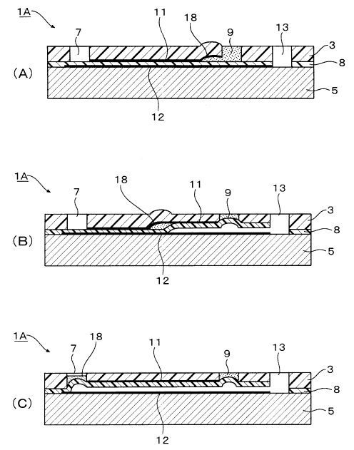
[0043] [FIG. lA] FIG. lA is an outline transparent plan view showing an
example of the micro passage chip used to implement the fluid transferring
method of the present invention.
[FIG. 1B] FIG. 1B is a sectional view taken through FIG. lA along line 1B-
1B.
[FIG. 2] FIG. 2 is a set of schematic sectional views showing the principle
of the fluid transferring method of the present invention using the micro
passage
chip 1A shown in FIGS. lA and 1B.
- 16 -
CA 02656686 2008-12-30
[FIG. 3] FIG. 3 is a flowchart illustrating an exemplary method of forming
a non-adhesive thin-film layer that is used in the micro passage chip of the
present invention.
[FIG. 4] FIG. 4 is a set of exploded perspective views showing the micro
passage chip lA shown in FIGS. 1A and 1B.
[FIG. 5] FIG. 5 is an outline sectional view showing another embodiment
of the micro passage chip used to implement the fluid transferring method of
the
present invention.
[FIG. 6] FIG. 6 is a set of outline sectional views showing the principle of
transferring a fluid using the micro passage chip 1B shown in FIG. 5.
[FIG. 7] FIG. 7 is an outline sectional view showing yet another
embodiment of the micro passage chip used to implement the fluid transferring
method of the present invention.
[FIG. 8] FIG. 8 is an outline sectional view showing the principle of
transferring a fluid using the micro passage chip 1C shown in FIG. 7.
[FIG. 9] FIG. 9 is a set of plan views showing exemplary layouts of a first
non-adhesive thin-film layer 11, a second non-adhesive thin-film layer 12, and
a
third non-adhesive thin-film layer 17 in the micro passage chip 1C shown in
FIG.
7.
[FIG. l0A] FIG. 10A is an outline plan view showing an example of the
conventional micro-channel chip.
[FIG. lOB] FIG. 10B is a sectional view taken through FIG. 10A along line
lOB-10B.
LEGEND
[0044] lA, 1B, 1C micro passage chip according to the present invention
3 upper substrate
lower substrate
6 enlarged region
- 17 -
CA 02656686 2008-12-30
7, 9 port
8 intermediate substrate
11 first non-adhesive thin-film layer (non-adhesive thin-film
layer for a channel)
12 second non-adhesive thin-film layer (non-adhesive thin-film
layer for squeezing)
13 pressurizing port
15 hollow, concave channel
17 third non-adhesive thin-film layer (non-adhesive thin-film
layer for squeezing)
18 fluid (liquid)
19 pressurizing port
20 mask
100 conventional micro-channel chip
102 upper substrate
104 micro-channel
105, 106 port
108 lower substrate
BEST MODES FOR CARRYING OUT THE INVENTION
[0045] FIG. 1A is an outline transparent plan view showing an example of the
micro passage chip used to implement the fluid transferring method of the
present invention and FIG. lB is a sectional view taken through FIG. lA along
line 1B-lB. The micro passage chip 1A according to this embodiment comprises
basically a first substrate 3, a second substrate 5, and an intermediate
substrate
8 interposed between the first substrate 3 and the second substrate 5. In the
illustrated micro passage chip lA, the first substrate 3 is on the upper side
and
hence called "the upper substrate" whereas the second substrate 5 is on the
lower side and hence called "the lower substrate" for the sake of convenience.
- 18 -
CA 02656686 2008-12-30
Therefore, the relationship between the first (or second) substrate and the
upper
(or lower) substrate is arbitrary and by no means fixed.
[0046] The lower side of the upper substrate 3 is provided with a non-adhesive
thin-film layer for a channel (a first non-adhesive thin-film layer) 11 in a
specified area to cover a specified width and length. While the non-adhesive
thin-film layer for a channel 11 is fastened to the lower side of the upper
substrate 3, the interface between the non-adhesive thin-film layer for a
channel
11 and the intermediate substrate 8 is maintained in a non-adhesive state.
This
non-adhesive part is called the first non-adhesive part. As will be described
later
in detail, the first non-adhesive part should serve as a channel for a fluid.
One
end of the non-adhesive thin-film layer for a channel 11 is connected to a
port 7
and the other end to a port 9, both ports being open to the outer surface of
the
upper substrate 3. The ports are not limited to the illustrated mode where
they
are provided at opposite ends. Other possible modes are such that only one
port
is provided in an end portion of the non-adhesive thin-film layer for a
channel 11
or that a plurality of ports are provided not only at opposite ends but also
halfway of the non-adhesive thin-film layer for a channel 11. The port(s) are
used as an inlet and an outlet of fluids such as a liquid or gas. In the
present
invention, the term "liquid" is used to have such a meaning that it covers all
liquid phases including pure liquids as well as solutions, gels, sols, and
semi-
fluid phases. As will be described later in detail, when pressure is exerted
through the port 7 or 9, that part of the upper substrate which corresponds to
the
first non-adhesive part at the interface between the non-adhesive thin-film
layer
for a channel 11 and the intermediate substrate 8 inflates to form a channel
having a certain capacity. Thus, before the pressurization, the first non-
adhesive
part at the interface between the non-adhesive thin-film layer for a channel
11
and the intermediate substrate 8 has no capacity.
[0047] The upper side of the lower substrate 5 has a non-adhesive thin-film
layer
for squeezing 12 (a second non-adhesive thin-film layer) provided in a
specified
- 19 -
CA 02656686 2008-12-30
area to cover a specified width and length. While the non-adhesive thin-film
layer for squeezing 12 is fastened to the upper side of the lower substrate 5,
the
interface between the non-adhesive thin-film layer for squeezing 12 and the
intermediate substrate 8 is maintained in a non-adhesive state. This non-
adhesive part is called the second non-adhesive part. As will be described
later
in detail, the second non-adhesive part should serve as a squeezing means for
transferring a fluid. One end of the non-adhesive thin-film layer for
squeezing
12 is connected to a pressurizing port 13 that is open to the outer surface of
the
upper substrate 3. The pressurizing port 13 may be provided in such a way that
it is open to the outer surface of the lower substrate 5. If desired, the
pressurizing port 13 may be provided halfway, rather than in an end portion,
of
the non-adhesive thin-film layer for squeezing 12. The non-adhesive thin-film
layer for squeezing 12 may be as long as the non-adhesive thin-film layer for
a
channel 11 or it may be shorter or longer than the latter. Thus, the length of
the
non-adhesive thin-film layer for squeezing 12 may be selected as appropriate
for
its use. What is important in the present invention is that the non-adhesive
thin-film layer for squeezing 12 should be provided in such a way that it lies
either above or under the non-adhesive thin-film layer for a channel 11, with
the
intermediate substrate 8 lying in between. Unless the non-adhesive thin-film
layer for squeezing 12 is provided in such a way that it lies either above or
under
the non-adhesive thin-film layer for a channel 11, with the intermediate
substrate 8 lying in between, the intermediate substrate 8 in the area that
corresponds to the second non-adhesive part in the area where the non-adhesive
thin-film layer for squeezing 12 is present will not be able to inflate to
perform
the transfer-by-squeeze function; for details, see below. Other possible modes
are
such that the entire portion of the non-adhesive thin-film layer for squeezing
12
lies either above or under the non-adhesive thin-film layer for a channel 11
or
that only a portion of the non-adhesive thin-film layer for squeezing 12 lies
either above or under the non-adhesive thin-film layer for a channel 11. When
- 20 -
CA 02656686 2008-12-30
pressure is exerted through the pressurizing port 13, that part of the
intermediate substrate 8 which corresponds to the second non-adhesive part at
the interface between the non-adhesive thin-film layer for squeezing 12 and
the
intermediate substrate inflates to form a space having a certain capacity, but
before the pressurization, the second non-adhesive part at the interface
between
the non-adhesive thin-film layer for squeezing 12 and the intermediate
substrate
8 has no capacity.
[0048] FIG. 2 is a set of schematic sectional views showing the principle of
the
fluid transferring method of the present invention using the micro passage
chip
1A shown in FIGS. 1A and 1B. Reference is first made to FIG. 2A. Suppose a
fluid of interest (say, a liquid 18) is injected through the port 9. The
method and
means of injection are not limited in any particular way. Methods and means of
injection under pressure that are known to and conventionally used by skilled
artisans can be appropriately chosen for use. By injecting the liquid 18, that
part of the upper substrate which corresponds to the first non-adhesive part
at
the interface between the non-adhesive thin-film layer for a channel 11 and
the
intermediate substrate 8 inflates to form a gap having a certain capacity and,
as
a result, an appropriate amount of the liquid 18 is accommodated in the gap.
Reference is next made to FIG. 2B. Using a tool such as a syringe (not shown),
a
pressurizing fluid is forced in through the pressurizing port 13. What can be
utilized as the pressurizing fluid is selected from among a variety of gases
such
as air, a variety of liquids such as water, and a variety of oils such as
mineral
oils. The pressurizing fluid gets into the second non-adhesive part between
the
lower side of the intermediate substrate 8 and the non-adhesive thin-film
layer
for squeezing 12 on the upper side of the lower substrate 5, whereby the
intermediate substrate 8 inflates. As the inflating nose of the intermediate
substrate 8 advances, the liquid 18 that is closer to the port 9 is squeezed
and
transferred toward the port 7. Finally, reference is made to FIG. 2C. As the
pressurizing fluid is kept forced in, the inflating nose of the intermediate
- 21 -
CA 02656686 2008-12-30
substrate 8 eventually reaches the port 7, whereupon the liquid 18 is
completely
squeezed so that it can be transferred to the port 7 which is the intended
area.
This procedure may be utilized, for example, in the case where the product of
PCR amplification of a DNA sample is transferred to a different step of
analysis.
In addition, by repeating the steps shown in FIGS. 2A to 2C, a specified
amount
of the liquid 18 can be transferred to the port 7. Except in the area where
the
non-adhesive thin-film layer for a channel 11 is present, the upper substrate
3 is
adhered to the intermediate substrate 8, so the liquid 18 will not diffuse to
the
interface between the upper substrate 3 and the intermediate substrate 8 in
any
areas other than where the non-adhesive thin-film layer for a channel 11 is
present.
[0049] The non-adhesive thin-film layer 11 and/or the non-adhesive thin-film
layer 12 in the micro passage chip to be used in the present invention may be
exemplified by the following that can be formed by known conventional
techniques of chemical thin film formation: electrode film, dielectric
protective
film, semiconductor film, transparent conductive film, fluorescent film,
superconductive film, dielectric film, solar cell film, anti-reflective film,
wear-
resistant film, optical interfering film, reflective film, antistatic film,
conductive
film, anti-fouling film, hard coating film, barrier film, electromagnetic wave
shielding film, IR shield film, UV absorption film, lubricating film, shape-
memory film, magnetic recording film, light-emitting device film,
biocompatible
film, corrosion-resistant film, catalytic film, gas sensor film, etc.
[0050] The chemical thin-film forming means for forming the non-adhesive thin-
film layer 11 and/or the non-adhesive thin-film layer 12 may be exemplified by
the method of forming a thin film with an apparatus for plasma discharge
treatment, preferably using a organofluorine compound or a metal compound as
the reactive gas.
[0051] Exemplary organofluorine compounds that can be used in this thin-film
forming method include: fluorocarbon compounds such as methane fluorides
- 22 -
CA 02656686 2008-12-30
(e.g., fluoromethane, difluoromethane, trifluoromethane, and
tetrafluoromethane), ethane fluorides (e.g., hexafluoroethane), 1,1,2,2-
tetrafluoroethylene, 1,1,1,2,3,3,-hexafluoropropane, hexafluoropropane, and 6-
fluoropropylene; fluorohydrocarbon compounds such as 1,1-difluoroethylene,
1, 1, 1, 2 -tetrafluoroethane, and 1,1,2,2,3-pentafluoropropane;
chlorofluorohydrocarbon compounds such as difluorodichloromethane and
triflurochloromethane; fluoroalcohols such as 1,1,1,3,3,3-hexafluoro-2-
propanol,
1,3-difluoro-2-propanol, and perfluorobutanol; fluorocarboxylate esters such
as
vinyl trifluoroacetate and 1,1,1-trifluoroacetate; and ketone fluorides such
as
acetyl fluoride, hexafluoroacetone, and 1,1,1-trifluoroacetone.
Trifluoromethane
is preferred.
[0052] Exemplary metal compounds that can be used in this thin-film forming
method include elementary or alloyed metal compounds or organometallic
compounds of Al, As, Au, B, Bi, Ca, Cd, Cr, Co, Cu, Fe, Ga, Ge, Hg, In, Li,
Mg,
Mn, Mo, Na, Ni, Pb, Pt, Rh, Sb, Se, Si, Sn, Ti, V, W, Y, Zn, Zr, etc.
[0053] Another chemical film forming technique that may be employed is the
formation of a dense film by the sol-gel method and examples of the metal
compounds that are preferred for use in this method include elementary or
alloyed metal compounds or organometallic compounds of Al, As, Au, B, Bi, Ca,
Cd, Cr, Co, Cu, Fe, Ga, Ge, Hg, In, Li, Mg, Mn, Mo, Na, Ni, Pb, Pt, Rh, Sb,
Se, Si,
Sn, Ti, V, W, Y, Zn, Zr, etc.
[0054] The non-adhesive thin-film layer 11 and/or the non-adhesive thin-film
layer 12 can also be formed by methods other than those mentioned above. For
instance, the non-adhesive thin-film layer 11 can be formed on the lower side
of
the upper substrate 3 and the non-adhesive thin-film layer 12 on the upper
side
of the lower substrate 5 by printing. Printing can be done by adopting a
variety
of known and conventional printing methods, including roll printing, silk
printing, pattern printing, decalcomania, electrostatic duplication, and the
like.
If the non-adhesive thin-film layer 11 and/or the non-adhesive thin-film layer
12
- 23 -
CA 02656686 2008-12-30
is to be formed by printing techniques, various materials can advantageously
be
used to form the non-adhesive thin-film layer 11 and/or the non-adhesive thin-
film layer 12 and they include: fine metal particles (for example, the fine
particles of elementary metals or alloys thereof as selected from among Al,
As,
Au, B, Bi, Ca, Cd, Cr, Co, Cu, Fe, Ga, Ge, Hg, In, Li, Mg, Mn, Mo, Na, Ni, Pb,
Pt,
Rh, Sb, Se, Si, Sn, Ti, V, W, Y, Zn, Zr, etc. or the fine particles of oxides
of these
elementarv metals or alloys thereof (e.g. fine ITO particles), and the fine
particles of organometallic compounds of these metals), conductive ink,
insulated
ink, fine carbon particles, silanizing agent, parylene, coatings, pigments,
dyes,
water-based dye ink, water-based pigment ink, oil-based dye ink, oil-based
pigment ink, solvent-based ink, solid ink, gel ink, polymer ink, and the like.
[0055] Alternatively, the non-adhesive thin-film layer 11 and/or the non-
adhesive
thin-film layer 12 can be formed by a spray coating technique. For example, a
coating agent may be sprayed from above a mask having a specified channel
pattern and then dried to form the non-adhesive thin-film layer 11 on the
lower
side of the upper substrate 3 and the non-adhesive thin-film layer 12 on the
upper side of the lower substrate 5. For example, materials capable of forming
coats such as an electrode coat, a dielectric protective coat, a semiconductor
coat,
a conductive coat, a fluorescent coat, a superconductive coat, a dielectric
coat, an
anti-reflective coat, a wear-resistant coat, an optical interfering coat, a
reflective
coat, an antistatic coat, an anti-fouling coat, a hard coat, a barrier coat,
an
electromagnetic wave shielding coat, an IR shield coat, an UV absorption coat,
a
lubricating coat, a light-emitting device coat, a biocompatible coat, a
corrosion-
resistant coat, a catalytic coat, a metal coat, a glass coat, a paint coat, a
water-
repellant coat, a hydrophilic coat, a resin coat, a rubber coat, a synthetic
fiber
coat, a synthetic resin coat, a phospholipid coat, a coat formed by organism-
derived materials, a biomaterial adhesion preventing coat, a lipid coat, an
oil
coat, a silane compound coat, a silazane compound coat, and an adhesive coat,
may be dissolved or suspended in suitable solvents, with the resulting
solution or
- 24 -
CA 02656686 2008-12-30
suspension being sprayed as a coating agent. The water-repellant coat using a
silicone acrylic resin based water repellant is preferred.
[0056] The film thickness of the non-adhesive thin-film layer 11 and/or the
non-
adhesive thin-film layer 12 varies with the thin-film forming method employed
and it is generally preferred to lie within the range from 10 nm to 300 gm. If
the
film thickness of the non-adhesive thin-film layer 11 and/or the non-adhesive
thin-film layer 12 is less than 10 nm, these thin-film layers will not be
formed
uniformly but both adhesive and non-adhesive sites will be scattered about as
islands, making it difficult to attain the intended objects of the present
invention. If, on the other hand, the film thickness of the non-adhesive thin-
film
layer 11 and/or the non-adhesive thin-film layer 12 is greater than 300 m,
not
only is the non-adhering effect saturated but due to the excessive thickness
of
these layers, two adjacent substrates also come apart at the border to the non-
adhesive thin-film layer 11 or 12 and fail to be bonded effectively. This
causes
undesirable inconveniences such as the failure to maintain the exact width of
the
non-adhesive thin-film layer 11 and/or the non-adhesive thin-film layer 12. If
the chemical thin-film forming method is used, the film thickness of the non-
adhesive thin-film layer 11 is generally within the range from 10 nm to 10 m,
preferably within the range from 30 nm to 5 m, more preferably within the
range froni 50 nm to 3 gm. If the spray coating method is used, the film
thickness of the non-adhesive thin-film layer 11 is generally within the range
from 50 nm to 300 m, preferably within the range from 80 m to 200 m, more
preferably within the range from 100 nm to 100 m. If the printing method is
used, the film thickness of the non-adhesive thin-film layer 11 is generally
within
the range from 500 nm to 100 m, preferably within the range from 800 nm to 80
m, more preferably within the range from 1 m to 50 m.
[0057] The width of the non-adhesive thin-film layer 11 and/or the non-
adhesive
thin-film layer 12 may generally be the same as or greater or even smaller
than
the width of the micro-channel in the conventional micro-channel chip.
- 25 -
CA 02656686 2008-12-30
Generally, the non-adhesive thin-film layer 11 and/or the non-adhesive thin-
film
layer 12 has a width ranging from about 10 m to about 3000 m. If the width
of
the non-adhesive thin-film layer 11 and/or the non-adhesive thin-film layer 12
is
less than 10 m, such a high pressure must be exerted to inflate the non-
adhesive part that the micro-channel chip 1 itself might be destroyed. If, on
the
other hand, the width of the non-adhesive thin-film layer 11 and/or the non-
adhesive thin-film layer 12 exceeds 3000 m, undesirable excessive saturation
will occur although the micro-channel chip is inherently intended to transport
and control very small amounts of liquid or gas and perform chemical reaction,
synthesis, purification, extraction, generation and/or analysis on substances.
It
is generally preferred that the non-adhesive thin-film layer 12 is wider than
the
non-adhesive thin-film layer 11. The greater the width, the higher the
pressure
that can be applied and this allows for positive transfer by squeezing.
[0058] The pattern itself of the non-adhesive thin-film layer for a channel 11
is
by no means limited to the illustrated linear form. In consideration of the
object
and/or use, the non-adhesive thin-film layer 11 in Y-shaped, L-shaped, S-
shaped,
X-shaped or various other patterns may be adopted. In addition to the linear
portion, the non-adhesive thin-film layer 11 may also have an enlarged region
in
any planar shape, such as a circular, an elliptical, a rectangular, or a
polygonal
shape. The enlarged region can function as a liquid reservoir upon inflating;
this
liquid reservoir portion may be utilized to ensure efficient performance of
PCR
amplification and other operations.
[0059] The pattern itself of the non-adhesive thin-film layer for squeezing 12
is
by no means limited to the illustrated rectangular linear form. Depending on
the
shape of the non-adhesive thin-film layer for a channel 11 that is superposed
on
it, with the intermediate substrate 8 lying in between, any other pattern such
as
a streamlined, a diamond-like or a polygonal shape may be adopted. In
addition,
the pattern of the non-adhesive thin-film layer for squeezing 12 suffices to
overlap with at least a portion of the pattern of the overlying non-adhesive
thin-
- 26 -
CA 02656686 2008-12-30
film layer for a channel 11 and the two patterns do not necessarily overlap in
all
parts. In short, the overlap may be in the necessary and sufficient amount
that
can attain the intended transfer by squeezing.
[0060] The upper substrate 3 of the micro passage chip 1 that is used in the
present invention is preferably made of an elastic and/or flexible polymer or
elastomer. If the upper substrate 3 is not formed of an elastic and/or
flexible
material, it becomes either impossible or difficult to ensure that the part of
the
upper substrate 3 which corresponds to the non-adhesive thin-film layer for a
micro-channel 11 is sufficiently deformed to create a micro-channel of the
type
found in the conventional micro-channel chip. Hence, preferred materials of
which the upper substrate 3 can be formed include not only silicone rubbers
such
as polydimethylsiloxane (PDMS) but also the following: nitrile rubber,
hydrogenated nitrile rubber, fluorinated rubber, ethylene-propylene rubber,
chloroprene rubber, acrylic rubber, butyl rubber, urethane rubber,
chlorosulfonated polyethylene rubber, epichlorohydrin rubber, natural rubber,
isoprene rubber, styrene-butadiene rubber, butadiene rubber, polysulfide
rubber,
norbornene rubber, and thermoplastic elastomers. Silicone rubbers such as
polydimethylsiloxane (PDMS) are particularly preferred.
[0061] It is generally preferred that the thickness of the upper substrate 3
is
within the range from 10 gm to 5 mm. If the thickness of the upper substrate 3
is less than 10 m, even a low pressure is sufficient for creating a micro
passage
by inflating that part of the upper substrate 3 which corresponds to the non-
adhesive thin-film layer 11 but, on the other hand, there is a high likelihood
for
the upper substrate 3 to rupture. If the thickness of the upper substrate 3
exceeds 5 mm, an undesirably high pressure must be exerted to create a micro-
channel by inflating that part of the upper substrate 3 which corresponds to
the
non-adhesive thin-film layer 11.
[0062] The intermediate substrate 8 of the micro-channel chip 1A that is used
in
the present invention is preferably made of an elastic and/or flexible polymer
or
- 27 -
CA 02656686 2008-12-30
elastomer. If the intermediate substrate 8 is not formed of an elastic and/or
flexible material, it becomes either impossible or difficult to ensure that
the part
of the intermediate substrate 8 which corresponds to the non-adhesive thin-
film
layer for squeezing 12 is sufficiently deformed to inflate and realize
transfer by
squeezing. Hence, preferred materials of which the intermediate substrate 8
can
be formed. include not only silicone rubbers such as polydimethylsiloxane
(PDMS) but also the following: nitrile rubber, hydrogenated nitrile rubber,
fluorinatecl rubber, ethylene-propylene rubber, chloroprene rubber, acrylic
rubber, butyl rubber, urethane rubber, chlorosulfonated polyethylene rubber,
epichlorohydrin rubber, natural rubber, isoprene rubber, styrene-butadiene
rubber, butadiene rubber, polysulfide rubber, norbornene rubber, and
thermoplastic elastomers. Silicone rubbers such as polydimethylsiloxane
(PDMS) are particularly preferred. If the upper substrate 3 is formed of PDMS,
it is preferred that the intermediate substrate 8 is also formed of PDMS. Two
members of PDMS can be adhered strongly to each other without using any
adhesive. This phenomenon is generally called "permanent bonding." The term
permanent bonding as used herein refers to such a property that two substrates
containing Si as a component that constitute them can be adhered to each other
without using an adhesive but by just performing a certain kind of surface
modification; this property contributes to exhibiting an effective seal on
micro-
structures in micro-channel chips. In the permanent bonding of PDMS
substrates, their mating surfaces are subjected to an appropriate treatment
for
surface modification and then the two substrates are superposed, with the
mating surfaces of the two substrates placed in intimate contact with each
other,
and the assembly is left to stand for a certain period of time, whereupon the
two
substrates can be easily adhered together. In other words, those parts of the
substrates where the non-adhesive thin-film layer 11 is present are not
permanently bonded but are maintained in a non-adhesive state, so upon
application of pressure or the like, they can be inflated to deform into a
balloon-
- 28 -
CA 02656686 2008-12-30
like shape, thereby creating a gap for a channel. Since the parts of the
substrates other than where the non-adhesive thin-film layer 11 is present are
permanently bonded, the liquid or gas that is passed through the inflated
portion
will not leak to any other sites.
[0063] It is generally preferred that the thickness of the intermediate
substrate 8
is within the range from 10 m to 500 m. If the thickness of the intermediate
substrate 8 is less than 10 gm, even a low pressure is sufficient to provide
ease in
inflating the second non-adhesive part which corresponds to the non-adhesive
thin-film layer 12 but, on the other hand, there is a high likelihood for the
intermediate substrate 8 to rupture. If the thickness of the intermediate
substrate 8 exceeds 500 m, an undesirably high pressure must be exerted to
inflate the second non-adhesive part which corresponds to the non-adhesive
thin-
film layer 12.
[0064] The lower substrate 5 of the micro passage chip according to the
present
invention has no particular need to be elastic and/or flexible but it is
preferred to
be capable of strong adhesion to the intermediate substrate 8. Suppose the
intermediate substrate 8 is made of polydimethylsiloxane (PDMS); if the lower
substrate 5 is made of PDMS or glass, the intermediate substrate 8 and the
lower substrate 5 can be permanently bonded to each other without using an
adhesive. Thus, those parts of the substrates where the non-adhesive thin-film
layer 12 is present are not permanently bonded but are maintained in a non-
adhesive state, so upon application of pressure or the like, they can be
inflated to
deform into a balloon-like shape, thereby creating a gap for squeezing. Since
the
parts of the substrates other than those where the non-adhesive thin-film
layer
12 is present are permanently bonded, the liquid or gas that is passed through
the inflated portions will not leak to any other sites. As long as it can be
adhered
to the intermediate substrate 8 to provide a bond that withstands the
inflating
pressure, the lower substrate 5 that is made of materials other than PDMS and
glass can of course be used. Examples of such lower substrate include
cellulose
- 29 -
CA 02656686 2008-12-30
ester substrates, polyester substrates, polycarbonate substrates, polystyrene
substrates, polyolefin substrates, etc.; specific examples of suitable
materials
include poly(ethylene terephthalate), poly(ethylene naphthalate),
polyethylene,
polypropylene, cellophane, cellulose diacetate, cellulose acetate butyrate,
cellulose acetate propionate, cellulose acetate phthalate, cellulose
triacetate,
cellulose nitrate, poly(vinylidene chloride), poly(vinyl alcohol), ethylene-
vinyl
alcohol, polycarbonate, norbornene resin, poly(methylpentene),
polyetherketone,
polyimide, polyethersulfone, poly(etherketone imide), polyamide,
fluoropolymer,
nylon, poly(methyl methacrylate), acrylics, polyarylate, etc. Other materials
that
can be used to form the lower substrate 5 include poly(lactic acid) resins,
poly(butylene succinate), nitrile rubber, hydrogenated nitrile rubber,
fluorinated
rubber, ethylene-propylene rubber, chloroprene rubber, acrylic rubber, butyl
rubber, urethane rubber, chlorosulfonated polyethylene rubber, epichlorohydrin
rubber, natural rubber, isoprene rubber, styrene-butadiene rubber, butadiene
rubber, polysulfide rubber, norbornene rubber, and thermoplastic elastomers.
These materials can be used either alone or in suitable admixture.
[0065] If these materials are not capable of permanent bonding by themselves,
their surfaces to be adhered to the intermediate substrate 8 are subjected to
such
a surface treatment that they can be permanently bonded. Preferred agents that
can be used in this surface treatment are silicon compounds and titanium
compounds and specific examples include: alkyl silanes such as dimethylsilane,
tetramethylsilane, and tetraethylsilane; organosilicon compounds such as
tetramethoxysilane, tetraethoxysilane, tetrapropoxysilane,
dimethyldiethoxysilane, methyltrimethoxysilane, and ethyltriethoxysilane;
silicon hydride compounds such as monosilane and disilane; silicon halide
compounds such as dichlorosilane, trichlorosilane, and tetrachlorosilane;
silazanes such as hexamethyldisilazane; and silicon compounds having
functional groups introduced therein, as exemplified by vinyl, epoxy, styryl,
- 30 -
CA 02656686 2008-12-30
methacryloxy, acryloxy, amino, ureido, chloropropyl, mercapto, sulfide, and
isocyanate.
[0066] It is generally preferred that the thickness of the lower substrate 5
is
within the range from 300 gm to 10 mm. If the thickness of the lower substrate
is less than 300 m, it becomes difficult to maintain the overall mechanical
strength of the micro passage chip. If, on the other hand, the thickness of
the
lower substrate 5 exceeds 10 mm, the mechanical strength required of the micro-
channel chip is saturated and only diseconomy results.
[0067] FIG. 3 is a flowchart illustrating an exemplary method of forming a non-
adhesive thin-film layer that is used in the micro passage chip of the present
invention. First, in step (a), a mask 20 is provided; it has a pattern formed
on it
that corresponds to the planar shape of the non-adhesive thin-film layer to be
formed. The mask may be formed of a synthetic resin film (e.g., PET film or
vinyl chloride film) or metal foil with a thickness of about 0.01 mm to 1 mm.
Therefore, by punching the film or metal foil through a mold die, or cutting
them
with a cutting tool, or performing electrical discharge machining with a
laser, or
machining by milling, a mask having a desired through-pattern can be
manufactured. In step (b), the mask 20 is attached to the upper side of a base
material (such as PDMS) that should serve as the upper substrate 3 or the
lower
substrate 5, either by utilizing a phenomenon such as adsorption or by
adhesion.
In step (c), the assembly is treated by an apparatus for plasma discharge
treatment in the presence of a reactive organofluorinated compound (e.g.,
trifluoromethane (CHF3)) to thereby coat the upper substrate 3 or the lower
substrate 5 with a thin fluorocarbon film in a pattern that corresponds to the
desired planar shape of the non-adhesive thin-film layer. In step (d), the
mask
20 is stripped, whereupon a fluorocarbon-made, non-adhesive thin-film layer is
left behind in a desired shape of pattern as it is fastened to the surface of
the
upper substrate 3 or the lower substrate 5. Alternatively, a common
commercially available waterproof spray made of a silicone acrylic resin based
- 31 -
CA 02656686 2008-12-30
water repellant is dusted or otherwise applied from above the mask 20 so that
the upper substrate 3 or the lower substrate 5 is coated with the silicone
acrylic
resin based water repellant in a pattern that corresponds to the planar shape
of
the non-adhesive thin-film layer to be formed, whereby the non-adhesive thin-
film layer 11 or 12 made of the silicone acrylic resin based water repellant
can be
formed.
[0068] If desired, the non-adhesive thin-film layer for a channel 11 and the
non-
adhesive thin-film layer for squeezing 12 may be provided on the intermediate
substrate 8. For instance, the non-adhesive thin-film layer for a channel 11
may
be provided on the upper side of the intermediate substrate 8 and the non-
adhesive thin-film layer for squeezing 12 on the lower side of the
intermediate
substrate 8, and yet the same advantage as described above is exhibited. By
thusly providing the non-adhesive thin-film layer for a channel 11 and the non-
adhesive thin-film layer for squeezing 12 on the opposite sides of the
intermediate substrate 8, the trouble of assuring registry that is required
when
positioning the non-adhesive thin-film layer for a channel 11 on the upper
substrate 3 and the non-adhesive thin-film layer for squeezing 12 on the lower
substrate 5 can be eliminated.
[0069] If desired, it is also possible to provide each of the non-adhesive
thin-film
layer for a channel 11 and the non-adhesive thin-film layer for squeezing 12
in
specified areas of the upper substrate 3, the lower substrate 5 and the
intermediate substrate 8. In this case, the non-adhesiveness of the upper
substrate to the intermediate substrate can be rendered more positive and so
can
be the non-adhesiveness of the lower substrate to the intermediate substrate,
with the resulting advantage that the parts that correspond to the non-
adhesive
thin-film layer for a channel 11 and the non-adhesive thin-film layer for
squeezing 12 will inflate even more easily upon application of a positive
pressure.
- 32 -
CA 02656686 2008-12-30
[0070] FIG. 4 is a set of exploded perspective views showing the micro passage
chip lA shown in FIGS. 1A and 1B. First, in step (1), the upper substrate 3,
the
lower substrate 5 and the intermediate substrate 8 are provided in preparation
for constructing the micro passage chip 1A. The upper substrate 3 and the
lower
substrate 5 are preliminarily treated by the method depicted in FIG. 3 to form
respective non-adhesive thin-film layers. The upper side of the lower
substrate 5
has the non-adhesive thin-film layer for squeezing 12 provided in a specified
area
to cover a specified width and length. The intermediate substrate 8 has a
through-hole 13a provided in a specified area. In addition, the lower side of
the
upper substrate 3 has the non-adhesive thin-film layer for a channel 11
provided
in a specified area to cover a specified width and length; it also has ports 7
and 9
provided as through-holes in such a way that they communicate with the
opposite ends of the non-adhesive thin-film layer for a channel 11; there is
also a
through-hole 13 that is provided in the position that corresponds to the
through-
hole 13a in the intermediate substrate 7 to serve as a pressurizing port. If
necessary, the upper side of the lower substrate 5, both sides of the
intermediate
substrate 8, and the lower side of the upper substrate 3 may be treated for
surface modification. By treatment for surface modification, the respective
substrates can be adhered to each other with greater strength. As a treatment
for surface modification, the oxygen plasma treatment, excimer UV light
irradiation or the like can be employed. The oxygen plasma treatment can be
performed in the presence of oxygen by means of an apparatus for plasma
discharge treatment. Excimer UV light irradiation can be performed in the air
at one atmosphere using a dielectric barrier discharge lamp, so it has the
advantage of low treatment cost. Next, in step (2), the lower side of the
intermediate substrate 8 is attached to the upper side of the lower substrate
5.
Finally, in step (3), the lower side of the upper substrate 3 is attached to
the
upper side of the intermediate substrate 8, whereupon the micro-channel chip
1A
is completed.
- 33 -
CA 02656686 2008-12-30
[0071] FIG. 5 is an outline sectional view showing another embodiment of the
micro passage chip used to implement the fluid transferring method of the
present invention. This micro passage chip 1B differs from the micro passage
chip 1A of FIG. 1 in that the first non-adhesive thin-film layer (non-adhesive
thin-film layer for a channel) 11 is replaced by a hollow, concave channel 15
that
is formed on that side of the upper substrate 3B which is the interface with
the
intermediate substrate 8, typically by the conventional photolithographic
technique. This concave channel 15 is used as a channel through which a liquid
is transferred. Provided in one end portion of the concave channel 15 to
communicate with it is a port 7 that is open to the outer surface of the upper
substrate 3B, and in addition, a port 9 that is open to the outer surface of
the
upper substrate 3B is provided halfway of the concave channel 15 to
communicate with it. As with the micro passage chip 1A, the upper side of the
lower substrate 5 has a non-adhesive thin-film layer for squeezing 12 (a
second
non-adhesive thin-film layer) provided in a specified area to cover a
specified
width and length. While the non-adhesive thin-film layer for squeezing 12 is
fastened to the upper side of the lower substrate 5, the interface between the
non-adhesive thin-film layer for squeezing 12 and the intermediate substrate 8
is
maintained in a non-adhesive state. This non-adhesive part is called the
second
non-adhesive part. As will be described later in detail, the second non-
adhesive
part should serve as a squeezing means for transferring a fluid. One end of
the
non-adhesive thin-film layer for squeezing 12 is connected to a pressurizing
port.
13 that is open to the outer surface of the upper substrate 3. The
pressurizing
port 13 may also be provided in such a way that it is open to the outer
surface of
the lower substrate 5. If desired, the pressurizing port 13 may be provided
halfway, rather than in an end portion, of the non-adhesive thin-film layer
for
squeezing 12. The non-adhesive thin-film layer for squeezing 12 may be as long
as the concave channel 15 or it may be shorter or longer than the latter.
Thus,
the length of the non-adhesive thin-film layer for squeezing 12 may be
selected
- 34 -
CA 02656686 2008-12-30
as appropriate for its use. What is important in the present invention is that
the
non-adhesive thin-film layer for squeezing 12 should be provided in such a way
that it lies either above or under the concave channel 15, with the
intermediate
substrate 8 lying in between. Unless the non-adhesive thin-film layer for
squeezing 12 is provided in such a way that it lies either above or under the
concave channel 15, with the intermediate substrate 8 lying in between, the
intermediate substrate 8 in the area that corresponds to the second non-
adhesive
part in the area where the non-adhesive thin-film layer for squeezing 12 is
present will not be able to inflate to perform the transfer-by-squeeze
function; for
details, see below. Other possible modes are such that the entire portion of
the
non-adhesive thin-film layer for squeezing 12 lies either above or under the
concave channel 15 or that only a portion of the non-adhesive thin-film layer
for
squeezing 12 lies either above or under the concave channel 15. When pressure
is exerted through the pressurizing port 13, that part of the intermediate
substrate 8 which corresponds to the second non-adhesive part at the interface
between the non-adhesive thin-film layer for squeezing 12 and the intermediate
substrate inflates to form a space having a certain capacity, but before the
pressurization, the second non-adhesive part at the interface between the non-
adhesive thin-film layer for squeezing 12 and the intermediate substrate 8 has
no capacity.
[0072] FIG. 6 is a set of outline sectional views showing the principle of
transferring a fluid using the micro passage chip 1B shown in FIG. 5. First,
as
shown in FIG. 6A, a fluid, say, a liquid 18 is injected through the port 9.
The
interior of the concave channel 15 is progressively filled with the liquid 18.
Then, as shown in FIG. 6B, pressure is applied through the pressurizing port
13
by means of a gas or liquid, whereupon the intermediate substrate 8 at the non-
adhesive interface (the second non-adhesive part) between the non-adhesive
thin-film layer for squeezing 12 and the intermediate substrate 8 begins to
inflate like a balloon along the sidewall surface of the concave channel 15.
By
- 35 -
CA 02656686 2008-12-30
controlling the pressure being applied through the pressurizing port 13, the
degree of inflation of the intermediate substrate 8 can be controlled and so
can be
the amount in which the liquid 18 overflows the port 7. Therefore, the micro
passage chip 1B can be used not only for the purpose of fluid transfer but
also for
weighing purposes. Finally, as shown in FIG. 6C, pressurization is continued
through the pressurizing port 13, whereupon the intermediate substrate 13
continues to inflate along the sidewall and ceiling surfaces of the concave
channel 15 until all of the liquid 18 within the concave channel 15 is pushed
through the port 7, whereupon its transfer is complete. Thus, with the micro
passage chip 1B, controlled fluid transfer can be implemented.
[0073] FIG. 7 is an outline sectional view showing yet another embodiment of
the
micro passage chip used to implement the fluid transferring method of the
present invention. The micro passage chip 1C differs from the micro
passage chip 1A of FIG. 1 in that two intermediate substrates, the first
and second ones, are interposed between the upper substrate 3 and the
lower substrate 5. The micro passage chip 1C is characterized in that
the non-adhesive thin-film layer for a channel is sandwiched between
two non-adhesive thin-film layers for squeezing, one above and the other
beneath. For the sake of convenience in explanation, the first
intermediate substrate shall be called an upper intermediate substrate
8U and the second intermediate substrate, a lower intermediate
substrate 8L. The first non-adhesive thin-film layer 11 which serves as
the non-adhesive thin-film layer for a channel is formed on either the
lower side of the upper intermediate substrate 8U or the upper side of
the lower intermediate substrate 8L or both. The opposite ends of the
non-adhesive thin-film layer for a channel 11 are connected to ports 7
and 9 that penetrate the upper substrate 3 and the upper intermediate
substrate 8U. The second non-adhesive thin-film layer 12 which serves
as the first non-adhesive thin-film layer for squeezing is formed on either
- 36 -
CA 02656686 2008-12-30
the upper side of the lower substrate 5 or the lower side of the lower
intermediate substrate 8L or both. A first pressurizing port 13 that is
open to the upper surface of the upper substrate 3 is connected to at
least one site on the second non-adhesive thin-film layer 12 which serves
as the first non-adhesive thin-film layer for squeezing. The third non-
adhesive thin-film layer 17 which serves as the second non-adhesive
thin-film layer for squeezing is formed on either the lower side of the
upper substrate 3 or the upper side of the upper intermediate substrate
8U or both. A second pressurizing port 19 that is open to the upper
surface of the upper substrate 3 is connected to at least one site on the
third non-adhesive thin-film layer 17 which serves as the second non-
adhesive thin-film layer for squeezing. The position where the second
pressurizing port 19 is provided shall be such that it does not overlap the
first pressurizing port 13. The first pressurizing port 13 and the second
pressurizing port 19 may also be provided in such a way that they are
open to the outer surface of the lower substrate 5.
[0074] FIG. 8 is an outline sectional view showing the principle of
transferring a
fluid using the micro passage chip 1C shown in FIG. 7. The liquid 18 injected
into the gap formed in the first non-adhesive part which corresponds to the
first
non-adhesive thin-film layer 11 at the interface between the upper
intermediate
substrate 8U and the lower intermediate substrate 8L advances in a specified
direction as it is squeezed by the inflating nose that has occurred in the
second
non-adhesive part which corresponds to the second non-adhesive thin-film layer
12 at the interface between the lower substrate 5 and the lower intermediate
substrate 8L. On this occasion, the third non-adhesive part which corresponds
to
the third non-adhesive thin-film layer 17 at the interface between the upper
substrate 3 and the upper intermediate substrate 8U may also be inflated so
that
the liquid 18 is transferred by the squeezing action of the two inflating
noses. In
an alternative mode of transfer by squeezing, only the second non-adhesive
part
- 37 -
CA 02656686 2008-12-30
which corresponds to the second non-adhesive thin-film layer 12 at the
interface
between the lower substrate 5 and the lower intermediate substrate 8L is
inflated but the third non-adhesive part which corresponds to the third non-
adhesive thin-film layer 17 at the interface between the upper substrate 3 and
the upper intermediate substrate 8U is not inflated, or vice versa, and
various
other modes of transfer by squeezing may be implemented. If desired, either
the
second non-adhesive part which corresponds to the second non-adhesive thin-
film layer 12 at the interface between the lower substrate 5 and the lower
intermediate substrate 8L is inflated or the third non-adhesive part which
corresponds to the third non-adhesive thin-film layer 17 at the interface
between
the upper substrate 3 and the upper intermediate substrate 8U may be inflated
so that it functions as a valve for opening or closing the gap formed in the
non-
adhesive part that corresponds to the first non-adhesive thin-film layer 11 at
the
interface between the upper intermediate substrate 8U and the lower
intermediate substrate 8L. Thus, with the micro passage chip 1C shown in FIG.
7, fluid transfer can be performed in extremely complicated ways including its
advancing, retracting and stopping.
[0075] FIG. 9 is a set of plan views showing exemplary layouts of the first
non-
adhesive thin-film layer 11, the second non-adhesive thin-film layer 12, and
the
third non-adhesive thin-film layer 17 in the micro passage chip 1C shown in
FIG.
7. FIG. 9A shows the layout of the third non-adhesive thin-film layer 17 at
the
interface between the upper substrate 3 and the upper intermediate substrate
8U, FIG. 9B shows the layout of the first non-adhesive thin-film layer 171 at
the
interface between the upper intermediate substrate 8U and the lower
intermediate substrate 8L, FIG. 9C shows the layout of the second non-adhesive
thin-film layer 12 at the interface between the lower substrate 5 and the
lower
intermediate substrate 8L, and FIG. 9D shows these three non-adhesive thin-
film layers combined together. As shown, the second non-adhesive thin-film
layer 12 and the third non-adhesive thin-film layer 17 independently overlap
in
- 38 -
CA 02656686 2008-12-30
some areas with the first non-adhesive thin-film layer 11 but in other areas
the
first non-adhesive thin-film layer 11 is sandwiched between the second non-
adhesive thin-film layer 12 and the third non-adhesive thin-film layer 17, one
above and the other beneath. This difference is based on the aforementioned
differences in object, such as whether the non-adhesive thin-film layers are
used
for squeezing or as a valve. In the embodiment under consideration, the first
non-adhesive thin-film layer 11 has five ports 9-1 to 9-5 through which the
fluid
is injected, as well as two ports 7-1 and 7-2 through which the fluid is
withdrawn. Numeral 6 indicates an enlarged region in the first non-adhesive
thin-film layer 11. This enlarged region 6 is utilized as a vessel in which
fluids
transferred by squeezing through the respective inlet ports are mixed under
agitation. The layout is such that when the fluids injected through the ports
9-1
to 9-5 are sequentially transferred by squeezing into the mixing/agitating
vessel
6, either one overlying or underlying squeezing gap is responsible for fluid
transfer to the site at which the channel formed by the first non-adhesive
thin-
film layer 11 divides into branches. Because of this layout, the fluid within
in
the channel formed by the first non-adhesive thin-film layer 11 can be
transferred in a desired direction. In addition, by providing squeezing gaps,
one
overlying and the other underlying, so that they hold the first non-adhesive
thin-
film layer 11 between themselves, the fluid within the channel formed by the
first non-adhesive thin-film layer 11 can be transferred without interruption
even if the squeezing gaps overlap each other when they are provided at the
site
where the channel formed by the first non-adhesive thin-film layer 11 divides
into branches or when they are provided in the middle of a long channel.
EXAMPLE 1
[0076] (1) Fabrication of a micro passage chip
According to the flowchart shown in FIG. 4, a micro passage chip 1A was
fabricated. First, two masks were prepared by cutting straight scores (feature
- 39 -
CA 02656686 2008-12-30
size, 400 gm) through PET films 0.025 mm thick. One of the masks was
intended for the first non-adhesive thin-film layer (the non-adhesive thin-
film
layer for a channel) 11 and the other mask was intended for the second non-
adhesive thin-film layer (the non-adhesive thin-film layer for squeezing) 12;
the
scores in the mask for the second non-adhesive thin-film layer 12 were longer
than those in the mask for the first non-adhesive thin-film layer 11. One of
the
masks was placed on the lower side of an upper substrate 3 with a thickness of
3
mm that was made of silicone rubber (PDMS) and it was then attached to this
silicone-rubber made upper substrate 3 by means of self-adsorption. The other
mask was placed on the upper side of a lower substrate 5 with a thickness of 3
mm that was made of silicone rubber (PDMS) and it was then attached to this
silicone-rubber made lower substrate 5 by means of self-adsorption.
Subsequently, the two assemblies were housed within an apparatus for plasma
discharge treatment in a reactive trifluoromethane (CHF3) gas atmosphere and a
thin fluorocarbon film was coated from above the masks. After the end of the
coating process, the assemblies were taken out of the apparatus for plasma
discharge treatment and stripped of the masks. As a result, a thin
fluorocarbon
film with a thickness not greater than 1 gm that corresponded to the first non-
adhesive thin-film layer 11 had been formed on the lower side of the silicone-
rubber made upper substrate 3 in a pattern that followed the mask pattern;
similarly, a thin fluorocarbon film with a thickness not greater than 1 gm
that
corresponded to the non-adhesive thin-film layer 12 had been formed on the
upper side of the silicone-rubber made lower substrate 5 in a pattern that
followed the mask pattern. Holes that should serve as ports 7 and 9 were bored
through the upper substrate 3 in the terminal end portions of the first non-
adhesive thin-film layer 11; further, a pressurizing port 13 was bored through
the upper substrate 3 in a specified area.
[0077] Further, the lower side of the silicone-rubber made upper substrate 3
and
the upper side of the silicone-rubber made lower substrate 5, as well as the
upper
- 40 -
CA 02656686 2008-12-30
and lower sides of a 100 m thick silicone-rubber made intermediate substrate
8
were subjected to a treatment for surface modification by an oxygen plasma in
the apparatus for plasma discharge treatment. Following the treatment for
surface modification, the upper side of the silicone-rubber made lower
substrate
on which the thin patterned fluorocarbon film 12 had been formed was
attached to the lower side of the silicone-rubber made intermediate substrate
8
with the through-hole in such a way that the through-hole would connect to an
end portion of the thin patterned film 12; further, the lower side of the
silicone-
rubber made upper substrate 3 was attached to the upper side of the silicone-
rubber made intermediate substrate 8 in the assembly in such a way that the
thin patterned film 11 would overlap the thin patterned film 12, whereby the
silicone-rubber made upper substrate 3, the silicone-rubber made intermediate
substrate 8 and the silicone-rubber made lower substrate 5 were permanently
bonded to each other. When the lower side of the silicone-rubber made upper
substrate 3 was attached to the upper side of the silicone-rubber made
intermediate substrate 8, care was taken to ensure that the through-hole in
the
silicone-rubber made intermediate substrate 8 would be in registry with the
pressurizing port 13 in the silicone-rubber made upper substrate 3.
[0078] (2) Liquid transfer test
In the micro passage chip lA fabricated in (1) above, the port 7 was
charged with 1 L of the DNA staining solution Cyber Green I and examined for
any fluorescence under a microscope. Since there was no DNA available at that
time, no fluorescence was observed. The port 9 was charged with 10 L of a
solution of human genome (DNA) in TE and air pressure (positive pressure) was
applied to the solution in the port 9 by means of a syringe connected to the
through-hole in an adapter. The pressure in the port 9 was gradually increased
and at the point in time when it exceeded 50 kPa, the end portion that was
closer
to the port 9 of the non-adhesive part of the interface between the upper
substrate 3 on which the thin patterned fluorocarbon film 11 had been formed
- 41 -
CA 02656686 2008-12-30
and the intermediate substrate 8 started to inflate to generate a gap. The
entrance of a small amount of the human genome (DNA) solution into the gap
was verified by the inflation of the outer surface of the upper substrate.
Thereafter, air pressure (positive pressure) was applied through the
pressurizing
port 13 by means of a syringe connected to the through-hole in an adapter. The
pressure in the pressurizing port 13 was gradually increased and at the point
in
time when it exceeded 60 kPa, the end portion that was closer to the
pressurizing
port 13 of the non-adhesive part of the interface between the lower substrate
5
on which the thin patterned fluorocarbon film 12 had been formed and the
intermediate substrate 8 started to inflate and it was visually confirmed that
the
inflating nose advanced toward the port 7. At the point in time when the
inflating nose reached the port 7, the liquid in the port 7 was inspected
again.
Examination under a fluorescence microscope showed the emission of
fluorescence from the fluorescent reagent that had intercalated into the DNA.
This demonstrated that the liquid in the port 9 could be transferred to the
port 7
by the squeezing action that resulted from an inflation of the non-adhesive
part
of the interface between the lower substrate 5 and the intermediate substrate
8.
EXA.MPLE 2
[0079] (1) Fabrication of a micro passage chip
According to the flowchart shown in FIG. 4, a micro passage chip 1A was
fabricated using the spray coating method. First, two masks were prepared by
cutting straight scores (feature size, 400 m) through PET films 0.025 mm
thick.
One of the masks was intended for the first non-adhesive thin-film layer (the
non-adhesive thin-film layer for a channel) 11 and the other mask was intended
for the second non-adhesive thin-film layer (the non-adhesive thin-film layer
for
squeezing) 12; the scores in the mask for the second non-adhesive thin-film
layer
12 were longer than those in the mask for the first non-adhesive thin-film
layer
11. One of the masks was placed on the lower side of an upper substrate 3 with
a
- 42 -
CA 02656686 2008-12-30
thickness of 3 mm that was made of silicone rubber (PDMS) and it was then
attached to this silicone-rubber made upper substrate 3 by means of self-
adsorption. The other mask was placed on the upper side of a lower substrate 5
with a thickness of 3 mm that was made of silicone rubber (PDMS) and it was
then attached to this silicone-rubber made lower substrate 5 by means of self-
adsorption. A common commercially available waterproof spray made of a
silicone acrylic resin based water repellant was applied from above the masks.
After the end of the spraying, the masks were removed. As a result, a silicone
acrylic resin based water repellant coat with a thickness of 1 m to 5 m was
formed on both the lower side of the silicone-rubber made lower substrate 3
and
the upper side of the silicone-rubber made lower substrate 5 in a pattern that
followed the mask pattern. This patterned, silicone acrylic resin based water
repellant coat is a part that should serve as a non-adhesive thin-film layer.
The
upper side of the PDMS lower substrate where the patterned, silicone acrylic
resin based water repellant coat had formed, the lower side of the PDMS upper
substrate where the patterned, silicone acrylic resin based water repellant
coat
had formed, and both sides of an intermediate substrate were treated for
surface
modification by an oxygen plasma in an apparatus for plasma discharge
treatment. After the treatment, the intermediate substrate was attached to the
upper side of the PDMS lower substrate where the patterned, silicone acrylic
resin based water repellant coat had formed, and further, the lower side of
the
silicone-rubber made upper substrate 3 was attached to the upper side of the
silicone-rubber made intermediate substrate 8 in the assembly such that the
patterned, silicone acrylic resin based water repellant coat 11 would lie over
the
patterned, silicone acrylic resin based water repellant coat 12, whereby the
silicone-rubber made upper substrate 3, the silicone-rubber made intermediate
substrate 8 and the silicone-rubber made lower substrate 5 were permanently
bonded to each other. When the lower side of the silicone-rubber made upper
substrate 3 was attached to the upper side of the silicone-rubber made
- 43 -
CA 02656686 2008-12-30
intermediate substrate 8, care was taken to ensure that the through-hole in
the
silicone-rubber made intermediate substrate 8 would be in registry with the
pressurizing port 13 in the silicone-rubber made upper substrate 3.
(2) Liquid transfer test
With the micro passage chip fabricated in (1) above, a test was conducted
to see whether a liquid could be transferred from one port to the other. The
port
9 was charged with 1 L of the DNA staining solution Cyber Green I and
examined for any fluorescence under a microscope. Since there was no DNA
available at that time, no fluorescence was observed. The port 7 was charged
with 10 L of a solution of human genome (DNA) in TE and air pressure
(positive pressure) was applied to the solution in the port 7 by means of a
syringe
connected to the through-hole in an adapter. The applied pressure was
gradually
increased and at the point in time when it exceeded 50 kPa, the end portion
that
was closer to the port 9 of the non-adhesive part of the interface between the
upper substrate 3 on which the non-adhesive part consisting of the patterned,
silicone acrylic resin based water repellant coat 11 had been formed and the
intermediate substrate 8 started to inflate to generate a gap. The entrance of
a
small amount of the human genome (DNA) solution into the gap was verified by
the inflation of the outer surface of the upper substrate. Thereafter, air
pressure
(positive pressure) was applied through the pressurizing port 13 by means of a
syringe connected to the through-hole in an adapter. The pressure in the
pressurizing port 13 was gradually increased and at the point in time when it
exceeded 60 kPa, the end portion that was closer to the pressurizing port 13
of
- 44 -
CA 02656686 2008-12-30
the non-adhesive part of the interface between the lower substrate 5 on which
the non-adhesive part consisting of the patterned, silicone acrylic resin
based
water repellant coat 12 had been formed and the intermediate substrate 8
started to inflate and it was visually confirmed that the inflating nose
advanced
toward the port 7. At the point in time when the inflating nose reached the
port
7, the liquid in the port 7 was inspected again. Examination under a
fluorescence microscope showed the emission of fluorescence from the
fluorescent
reagent that had intercalated into the DNA. This demonstrated that the liquid
in the port 9 could be transferred to the port 7 by the squeezing action that
resulted from an inflation of the non-adhesive part of the interface between
the
lower substrate 5 and the intermediate substrate 8.
EXAMPLE 3
[0080] (1) Fabrication of a micro passage chip
A micro passage chip of the structure shown in FIG. 1 was fabricated by
the printing process. The print side of a known conventional printing OHP
(overhead projector) polyester sheet (100 m thick) was surface modified by
the
oxygen plasma treatment method; thereafter, the surface-modified side was
coated with an aminosilanizing agent so that the print side of the OHP sheet
would be amenable to permanent bonding. Subsequently, a desired pattern
drawn on a personal computer was printed on the print side of the OHP sheet
with a laser printer. The OHP sheet had carbon black and pigments (principal
ingredients) printed in thicknesses of 1 m to 6 m with a feature size of 800
m.
- 45 -
CA 02656686 2008-12-30
This OHP sheet was used as the lower substrate 5. The upper substrate 3 and
the intermediate substrate 8 were the same as the upper substrate and the
intermediate substrate that were used in Example 1. The upper side of the
lower substrate (OHP sheet) having the pattern printed as a thin film, the
lower
side of the upper substrate 3 prepared in Example 1, and both sides of the
intermediate substrate were surface modified by the oxygen plasma treatment
method. Subsequently, the surface-modified sides were attached together to
fabricate the micro passage chip of the present invention.
(2) Fluid transfer test
With the micro passage chip fabricated in (1) above, a test was conducted
to see whether a liquid could be transferred from one port to the other, using
the
same method as described in Example 1. As a result, it was verified that the
test
solution could be transferred from the port 9 to the port 7. This demonstrated
that the liquid in the port 9 could be transferred to the port 7 by the
squeezing
action that resulted from an inflation of the non-adhesive part of the
interface
between the lower substrate 5 and the intermediate substrate 8 that consisted
of
the second non-adhesive thin-film pattern formed by the printing process.
EXAMPLE 4
[0081] (1) Fabrication of a micro passage chip
Micro passage chip 1B of the structure illustrated in FIG. 5 was
fabricated. First, the lower side of an upper substrate 3 with a thickness of
3
mm that was made of silicone rubber (PDMS) was processed by a conventional
- 46 -
CA 02656686 2008-12-30
photolithographic technique to form a concave channel 15 that was 400 m wide
and 100 m deep. A port 7 communicating with one end portion of this concave
channel was bored through the substrate from its outer side, and a port 9 also
communicating with the concave channel was pored through the substrate from
its outer side in a position that was slightly away from the other end portion
of
the concave channel toward the port 7. In accordance with the method described
in Example 1 above, the second non-adhesive thin-film layer with a feature
size
of 400 m was formed of a thin fluorocarbon film on the upper side of the
lower
substrate 5. Both sides of a silicone-rubber made intermediate substrate 8
with
a thickens of 50 m, the lower side of the upper substrate 3 and the upper
side of
the lower substrate 5 were treated for surface modification by an oxygen
plasma
in an apparatus for plasma discharge treatment. After the surface modification
treatment, the lower substrate 5, the intermediate substrate 8 and the upper
substrate 3 were assembled together to fabricate the micro passage chip 1B
shown in FIG. 5
(2) Fluid transfer test
With the micro passage chip IB fabricated in (1) above, a test was
conducted to see whether a liquid could be transferred from one port to the
other.
Red-colored water in a volume equivalent to a third of the total capacity of
the
concave channel 15 was injected through the port 9. At that point in time, no
part of the red water was found to have reached the port 7. Subsequently, a
positive pressure was gradually applied through the pressurizing port 13 and
at
the point in time when it exceeded 60 kPa, the non-adhesive part of the
- 47 -
CA 02656686 2008-12-30
intermediate substrate 8 that corresponded to the position of the second non-
adhesive thin-film layer 12 on the lower substrate 5 began to inflate into a
balloon shape. At that point in time, the pressure being applied was
controlled
and the behavior of the red water in the concave channel 15 was observed. At
the point in time when the applied pressure was about 70 kPa, the red water
began to overflow the port 7. The applied pressure was further increased and
at
the point in time when it was about 90 kPa, almost all of the red water
injected
into the concave channel 15 through the port 9 was recovered through the port
7.
This result verified that even in a micro passage chip having the conventional
concave channel, the transfer-by-squeeze mechanism that depends on inflating
the non-adhesive part of the intermediate substrate that consists of a non-
adhesive thin-film layer is useful.
EXAMPLE 5
[0082] (1) Fabrication of a micro passage chip
A micro passage chip 1B of the structure illustrated in FIG. 7 was
fabricated. First, three masks were prepared by cutting straight scores
(feature
size, 400 m) through PET films 0.025 mm thick. The first mask was intended
for the first non-adhesive thin-film layer (the non-adhesive thin-film layer
for a
channel) 11, the second mask was intended for the second non-adhesive thin-
film
layer (the first non-adhesive thin-film layer for squeezing) 12, and the third
mask was intended for the third non-adhesive thin-film layer (the second non-
adhesive thin-film layer for squeezing) 17; the scores in the mask for the
second
- 48 -
CA 02656686 2008-12-30
non-adhesive thin-film layer 12 and the mask for the third non-adhesive thin-
film layer 17 were longer than those in the mask for the first non-adhesive
thin-
film layer 11. The first mask was placed on the lower side of an upper
intermediate substrate 8U with a thickness of 100 m that was made of PDMS
and it was then attached to this upper intermediate substrate 8U by means of
self-adsorption. The second mask was placed on the lower side of an upper
substrate 3 with a thickness of 3 mm that was made of PDMS and it was then
attached to this upper substrate 3 by means of self-adsorption. The third mask
was placed on the upper side of a lower substrate 5 with a thickness of 3 mm
that was made of PDMS and it was then attached to this lower substrate 5 by
means of self-adsorption. Subsequently, the three assemblies were housed
within an apparatus for plasma discharge treatment in a reactive
trifluoromethane (CHF;;) gas atmosphere and a thin fluorocarbon film was
coated
from above the masks. After the end of the coating process, the assemblies
were
taken out of the apparatus for plasma discharge treatment and stripped of the
masks. As a result, a thin (1 m) fluorocarbon film had been formed on the
surface of each substrate in a pattern that followed the mask pattern.
[0083] Further, a PDMS-made lower intermediate substrate 8L with a thickness
of 100 m was provided and three substrates consisting of this lower
intermediate substrate as well as the upper substrate 3 and the lower
intermediate substrate 8U were subjected to a treatment for opening through-
holes in specified areas. Thereafter, the surface of each substrate was
treated for
modification by the same method as described in Example 1. After the surface
- 49 -
CA 02656686 2008-12-30
modification treatment, the upper side of the lower substrate 5 on which the
thin
patterned fluorocarbon film 12 had been formed was attached to the lower side
of
the lower intermediate substrate 8L with the through-hole in such a way that
the through-hole would connect to an end portion of the thin patterned film
12;
further, the lower side of the upper intermediate substrate 8U on which the
thin
patterned film 11 had been formed was attached to the upper side of the lower
intermediate substrate 8L in the assembly in such a way that the thin
patterned
film 11 would overlap the thin-patterned film 12; furthermore, the lower side
of
the upper substrate 3 on which the thin patterned film 17 had been formed was
attached to the upper side of the upper intermediate substrate 8U in such a
way
that the thin patterned film 11 would overlap the thin-patterned film 17,
whereby the respective substrates were permanently bonded to each other.
[0084] (2) Fluid transfer test
In the micro passage chip 1C fabricated in (1) above, the port 7 was
charged with 1 L of the DNA staining solution Cyber Green I and examined for
any fluorescence under a microscope. Since there was no DNA available at that
time, no fluorescence was observed. The port 9 was charged with 10 L of a
solution of human genome (DNA) in TE and air pressure (positive pressure) was
applied to the solution in the port 9 by means of a syringe connected to the
through-hole in an adapter. The pressure in the port 9 was gradually increased
and at the point in time when it exceeded 60 kPa, the non-adhesive part of the
interface between the upper intermediate substrate 8U on which the thin
patterned fluorocarbon film 11 had been formed and the lower intermediate
- 50 -
CA 02656686 2008-12-30
substrate 8L began to inflate, creating a gap. The entrance of a small amount
of
the human genome (DNA) solution into the gap was verified by the inflation of
the outer surface of the upper substrate. Thereafter, air pressure (positive
pressure) was applied through the pressurizing port 13 by means of a syringe
connected to the through-hole in an adapter. The pressure in the pressurizing
port 13 was gradually increased and at the point in time when it exceeded 65
kPa, the end portion that was closer to the pressurizing port 13 of the non-
adhesive part of the interface between the lower substrate 5 on which the thin
patterned fluorocarbon film 12 had been formed and the lower intermediate
substrate 8L started to inflate and it was visually confirmed that the
inflating
nose advanced toward the port 7. When the pressurization through the
pressurizing port 13 was suspended, the transfer of the DNA solution was
interrupted. Air pressure (positive pressure) was then applied through the
pressurizing port 19. The pressure in the pressurizing port 19 was gradually
increased and at the point in time when it exceeded 55 kPa, the end portion
that
was closer to the pressurizing port 19 of the non-adhesive part of the
interface
between the upper substrate 3 on which the thin patterned film 17 had been
formed and the upper intermediate substrate 8U started to inflate and the
inflating nose advanced toward the port 7, whereupon the DNA solution that had
stayed between the upper intermediate substrate 8U and the lower intermediate
substrate 8L began to move again for transfer toward the port 7. When
pressurization through the pressurizing port 13 was resumed, both the
inflating
nose between the lower substrate 5 and the lower intermediate substrate 8L and
- 51 -
CA 02656686 2008-12-30
the inflating nose between the upper substrate 3 and the upper intermediate
substrate 8U eventually reached the port 7 and at that point in time, the
liquid
in the port 7 was inspected again. Examination under a fluorescence microscope
showed the emission of fluorescence from the fluorescent reagent that had
intercalated into the DNA. This demonstrated that even with a micro passage
chip of a four-layer structure, the fluid in the port 9 could be transferred
to an
intended area.
INDUSTRIAL APPLICABILITY
[0085] While the method of the present invention for transferring fluids by
squeezing under pressure has been described above specifically with reference
to
its preferred embodiments, the present invention is by no means limited to
those
disclosed embodiments but various improvements and modifications are possible.
For instance, three or more intermediate substrates may be interposed or if
desired, the upper substrate may be provided with both a zero-capacity channel
for fluids as a non-adhesive part that consists of a non-adhesive thin-film
layer
and a hollow concave channel for fluids.
It should also be noted that the method of the present invention for
transferring fluids by squeezing is by no means limited to fluid transfer from
one
port to another. It can also be used in fluid transfer from one port to any
micro-
structural elements on another microchip (as exemplified by a micro passage, a
reaction vessel, a piezoelectric device, a fluid control device, a
metallization
pattern, and electrodes). Therefore, non-adhesive thin-film layers can be so
- 52 -
CA 02656686 2008-12-30
provided as to establish communication between the port at the start point and
any of such micro-structural elements.
According to the method of the present invention for transferring fluids by
squeezing, fluids can be positively transferred by merely adopting a simple
pressure applying operation and this contributes to a marked improvement in
the practical utility and economy of the inethod. As a result, the method of
the
present invention for transferring fluids by squeezing finds effective and
advantageous use in various fields including medicine, veterinary medicine,
dentistry, pharmacy, life science, foods, agriculture, fishery, and police
forensics.
In particular, the method of the present invention for transferring fluids by
squeezing is optimum for use as a micro passage chip in the fluorescent
antibody
technique, in-situ hybridization and the like, and it can be used
inexpensively in
a broad range of areas including testing for immunological diseases, cell
culture,
virus fixation, pathological test, cytological diagnosis, biopsy tissue
diagnosis,
blood test, bacteriologic examination, protein analysis, DNA analysis, and RNA
analysis.
- 53 -