Note: Descriptions are shown in the official language in which they were submitted.
CA 02657504 2009-01-13
WO 2008/017143 PCT/CA2007/001278
METHOD OF FABRICATING SEMICONDUCTOR DEVICES ON A GROUP IV
SUBSTR TE WITH CONTROLLED INTERFACE PROPERTIES
AND DIFFUSION TAILS
This application claims the benefit of priority of U.S. Provisional Patent
Application
No. 60/822,138 filed August 11, 2006, which is incorporated herein by
reference.
FIELD OF THE INVENTION
The present invention relates generally to the epitaxial deposition of
electronic and
opto-electronic devices. More particularly, the present invention relates to
the deposition of
III/V electronic and opto-electronic device structures on group IV substrates.
BACKGROUND OF THE INVENTION
The deposition of layer sequences for IIUV opto/electronic devices, such as
multi-
junction solar cells and light-emitting diodes (LEDs), on group IV substrates
is known. The
electronic and optical properties of such devices are being studied
extensively and the
correlation between these properties and the characteristics of the substrate-
epilayer interface
is receiving great attention. The reason for the attention given to the
substrate-epilayer
interface is that, for the most part, the performance of these devices is
determined by the
quality of this interface.
When depositing a IIUV material, for example GaAs, epitaxially on a group IV
substrate, for example Ge, the formation of the appropriate atomic layer
sequence of the
group III and group V layers is not readily established. The group IV sites
(Ge atoms) can
bond either group III or group V atoms. In practice, some areas of the group
IV substrate will
bond group III atoms and some other areas will bond group V atoms. The
boundary regions
between these different growth areas give rise to considerable structural
defects, such as anti-
phase domains, which adversely affect the performance of the device.
To curtail some of these undesired events, the group IV substrates are usually
vicinal
substrates with an off-cut angle ranging from 0-15 . These vicinal substrates
offer terraces and
CA 02657504 2009-01-13
WO 2008/017143 PCT/CA2007/001278
step edges where the atoms can attach with different bond configurations, thus
providing
greater order in the growth process.
In devices such as, for example, solar cells having III/V compounds
epitaxially
deposited on a group IV substrate, it is often desirable to create part of the
device itself in the
group IV substrate by diffusing, for example, a group V species in the group
IV substrate. As
an example, for solar cells, if a group V element is diffused in a p-type Ge
substrate, an n-type
region is formed, giving rise to a p-n junction. This p-n junction becomes
photo-active and
can be part of a single or multijunction solar cell. However, when depositing
the III/V
compound at typical process temperatures (500-750 C) on the Ge substrate, the
group V
element of the compound tends to diffuse, with little control, in the
substrate thereby making
the formation of a predictable p-n junction difficult. In cases involving Ge
substrates with a
pre-existing p-n junction, as could be the case in the hetero-integration of
Ill-V
opto/electronics on Ge, SiGe and SiC electronic circuits, the deposition of an
overlaying IIUV
compound can modify the doping profile of the pre-existing p-n junction
resulting in subpar
performance of the p-n junction and device. Consequently, the electrical
characteristics are
not easily controllable. In such situations, it can become quite difficult, if
not impossible, to
attain and maintain the desired doping profile and the electrical
characteristics of the
substrate's p-n junction, such electrical characteristics including, in the
case of solar cells, the
open circuit voltage (Voc). Furthermore, group IV atoms will diffuse from the
substrate into
the epitaxially deposited III/V layers. Hence, layers within the initial 0.5 -
l m of the III/V
layer sequence can be highly doped with the group IV element when the
excessive diffusion
of group IV atoms is not curtailed through the use of suitable nucleation
conditions and
materials. Group IV atoms like Si and Ge are, at moderate concentrations,
typically n-type
dopants in III/V semiconductor material. However, due to their amphoteric
nature these atoms
can cause a large degree of compensation (combined incorporation of n- and p-
type
impurities) when incorporated at concentrations much larger than 2x10¹⁸crri 3,
often leading to
a strong deterioration of electrical and optical properties of the host
semiconductor layer.
U.S. Patent No. 6,380,601 B 1 to Ermer et al., hereinafter referred to as
Ermer, teaches
deposition of GaInP on an n-doped interface layer on a p-type Ge substrate and
subsequent
deposition of a GaAs binary compound on the GaInP layer. The phosphorous of
the GaInP
-2-
CA 02657504 2009-01-13
WO 2008/017143 PCT/CA2007/001278
layer tends to not diffuse in the Ge substrate as deeply as the arsenic of a
GaAs layer would.
Thus, the phosphorous doping and subsequent deposition of the GaInP layer
allows better
control of the doping profile of the n-type layer of the Ge substrate and
consequently, leads to
a better control of the electrical characteristics of the p-n junction formed
in the Ge substrate.
However, the problem with having a GaInP interfacial layer at the Ge substrate
interface is
that the morphology of devices prepared under typical epitaxial process
conditions for these
materials is not ideal: defects often abound. It would appear that extreme
nucleation
conditions (temperature, deposition rate, group V overpressure) of the GaInP
interfacial layer
are required in order to obtain devices with suitable morphology.
It is, therefore, desirable to provide a method for fabricating semiconductor
devices
having a III/V compound epitaxially deposited on a group IV substrate under
typical epitaxial
process conditions, the devices having a suitable morphology and the method
allowing better
control over the optical and electrical interface properties as well as the
diffusion layer in the
group IV substrate.
SUMMARY OF THE INVENTION
It is an object of the present invention to obviate or mitigate at least one
disadvantage
of previous devices having epitaxial III/V layers on a group IV substrate.
In a first aspect, the present invention provides a semiconductor device
comprising a
group IV layer; and a nucleating layer formed on the group IV layer. The
nucleating layer
includes a Ill-V compound having at least aluminum (Al) as a group III element
and at least
one of arsenic (As), nitrogen (N) and antimony (Sb) as a group V element.
In a second aspect, the present invention provides a method of fabricating a
semiconductor structure on a group IV layer. The method comprises a step of
forming a
nucleating layer on the group IV layer, the nucleating layer including a Ill-V
compound
having at least aluminum (Al) as a group III element and at least one of
arsenic (As), nitrogen
(N) and antimony (Sb) as a group V element. The method further comprises a
step of forming
a first Ill-V compound layer on the nucleating layer.
-3-
CA 02657504 2009-01-13
WO 2008/017143 PCT/CA2007/001278
In a third aspect, the present invention provides a method of controlling the
doping
profile of a p-n junction formed in a group IV substrate. The method comprises
a step of
forming a nucleating layer on the group IV substrate, the nucleating layer
including a Ill-V
compound having at least aluminum (Al) as a group III element and at least one
of arsenic
(As), nitrogen (N) and antimony (Sb) as a group V element. The method further
comprises a
step of forming a Ill-V compound layer on the nucleating layer, the nucleating
layer for
controlling the diffusion of group V elements into the group IV substrate and
for controlling
the diffusion of group IV elements out of the group IV substrate.
Other aspects and features of the present invention will become apparent to
those
ordinarily skilled in the art upon review of the following description of
specific embodiments
of the invention in conjunction with the accompanying figures.
BRIEF DESCRIPTION OF THE DRAWINGS
Embodiments of the present invention will now be described, by way of example
only,
with reference to the attached Figures, wherein:
Fig. 1 is a side view of an embodiment of the present invention;
Figs. 2A and 2B are photographs of embodiments of the present invention with
different thickness of an AlAs nucleating layer;
Fig. 3 is a haze measurement of the embodiment of Fig. I as a function of
thickness of the AlAs nucleating layer;
Fig. 4 is a depiction of the deposition process of AlAs on a vicinal Ge
substrate;
Fig. 5 is a graph of SIMS data for different atomic species of the structure
of
the embodiment of Fig. 1 when the thickness of the AlAs layer is nil;
Fig. 6 is a graph of SIMS data for different atomic species of the structure
of
the embodiment of Fig. 1 when the thickness of the AlAs layer is 11.6 A;
-4-
CA 02657504 2009-01-13
WO 2008/017143 PCT/CA2007/001278
Fig. 7 is a flow chart of a method of the present invention;
Fig. 8 is a graph of SIMS data for Phosphorous as a function of the thickness
of AlAs for the structure of the embodiment of Fig. 1;
Fig. 9 is a graph of SIMS data for Arsenic as a function of the thickness of
AlAs for the structure of the embodiment of Fig. 1;
Fig. 10 is a graph of SIMS data for Ge as a function of the thickness of AlAs
for the structure of the embodiment of Fig. 1;
Fig. 11 shows the concentration of Phosphorous as a function sample depth for
four different thicknesses of AlAs for the structure of the embodiment of Fig.
1;
Fig. 12 shows the concentration of Arsenic as a function sample depth for four
different thicknesses of AlAs for the structure of the embodiment of Fig. 1;
Fig. 13 shows the concentration of Ge as a function sample depth for four
different thicknesses of AIAs for the structure of the embodiment of Fig. 1;
Fig. 14 is a current versus voltage plot of a photovoltaic cell having a
structure
similar to that shown in the embodiment of Fig. 1; and
Fig. 15 is a series of current versus voltage plots for photovoltaic cells
fabricated without an AlAs nucleation layer and photovoltaic cells fabricated
with an
AlAs nucleation layer.
DETAILED DESCRIPTION
Generally, the present invention provides a method for fabricating electronic
or opto-
electronic devices having a group IV substrate on which a IIUV layer structure
is deposited.
The method allows for the manufacturing of devices with improved morphology
and
-5-
CA 02657504 2009-01-13
WO 2008/017143 PCT/CA2007/001278
controlled doping profiles of group V constituents into the group IV substrate
and group IV
constituents into the III/V layers.
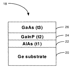
Fig. 1 shows an exemplary three junction semiconductor structure 18 embodying
the
present invention. Such a structure can be used in multi-junction solar cells,
e.g., three
junction solar cells. Further, as will be readily understood by a worker
skilled in the art,
similar structures can be used in light-emitting diodes (LEDs) and other
electronic and/or
opto-electronic devices. An AlAs layer 22 of thickness t, is deposited atop a
vicinal Ge
substrate 20. As will be understood by a worker having ordinary skill in the
art, the term
"vicinal" here refers to a crystal plane that is oriented near to a
fundamental plane. The angle
of the vicinal Ge substrate can range from 0 -20 ; the crystal orientation of
the Ge substrate
can be, for example, 6 towards the nearest <111> plane or any other suitable
orientation. On
top of the AlAs layer 22 are a GaInP layer 24 having a thickness t2 and a GaAs
layer 26
having a thickness t3. The deposition of the AlAs layer 22, the GaInP layer 24
and the GaAs
layer 26 can be achieved through any suitable means such as: metal organic
chemical vapor
deposition (MOCVD), chemical beam epitaxy (CBE), molecular beam epitaxy (MBE),
solid
phase epitaxy (SPE), hydride vapour phase epitaxy or by other similar hybrid
systems or
combinations thereof. Although a Ge substrate 20 is shown, any other suitable
group IV
substrates, such as, e.g., Si, SiGe or SiC substrates, can also be used.
Further, as will be
understood by the skilled worker, the above also applies in cases where,
instead of a group IV
substrate, a device requiring transition from a group IV material to a Ill-V
compound is used.
Similarly, the AlAs layer can be substituted, without departing from the scope
of the present
invention, with other Ill-V compound semiconductor alloys with a high
concentration of Al
such as, for example, AIN, AISb or Al(Ga)As.
In Figs. 2A and 2B, the morphology of the structure 18 is compared for two
different
thicknesses t1 of the A]As layer 22. In Figs 2A and 2B, a test structure 28
corresponds to the
structure 18 with t1=0 and a test structure 30 corresponds to test structure
18 with ti= 4
monolayers of AlAs. Figs. 2A and 2B show microscope photographs of the top
surface of
tests structures 28 and 30 where in each case t2=0.025 m and t3=0.2 m. The
test structures
28 and 30 were fabricated by MOCVD at temperatures ranging from 650-730 C
with the
-6-
CA 02657504 2009-01-13
WO 2008/017143 PCT/CA2007/001278
deposition rates of GaAs, GaInP and AlAs being respectively 4 m/hr, 0.8 m/hr
and 0.7-0.42
gm/hr.
As seen in Fig. 2A (GaInP on Ge), the number of defects, shown as white
speckles, is
much higher than if Fig. 2B (AlAs on Ge). The density of defects is of the
order of thousands
per cm2 in Fig. 2A and essentially 0 in Fig. 2B. This type of defect is
entirely absent on Fig.
2B. The large speckle in the central region of Fig. 2B it is attributed to a
foreign particle on
the test structure 30, which is not inherent to the nucleation process.
The graph of Fig. 3 shows a plot of haze for the structures 18 as a function
of tl, the
thickness of the AlAs layer 22. The measurement was performed with a
SurfscanTM haze
measurement apparatus manufactured by KLA-Tencor of California. It is very
clear from the
haze plot that adding just a fraction of a monolayer of AlAs greatly improves
the surface
morphology of the structure 18.
The reason for this improvement in the morphology of III/V compounds deposited
on
vicinal Ge substrates with an intermediate AlAs layer 22 between the
subsequent III/V
compounds is attributable to the following. As shown in Figs. 4A and 4B, Al
atoms are
relatively small with respect to As atoms. As such, the Al atoms have an
electro-chemical
potential that favors their positioning at the steps 40 present on the vicinal
Ge substrate 20.
Thus, introducing Al and As in the growth chamber and allowing sufficient time
to pass will
see the steps 40 predominantly occupied by Al atoms provided that the surface
energy is high
enough to allow surface reconfigurations due to the substrate temperature.
This allows for the
establishment of a homogeneous growth sequence, which leads to morphologically
sound
samples as shown in Fig. 2B in which the nucleation sequence as been properly
established
and therefore, the anti-phase domain defects have been greatly reduced. This
process is
known as a nucleation process and, in the case depicted in Figs. 4A and 4B,
can occur at
temperatures typical in depositing AlAs layer epitaxial layers (e.g., 650-730
C).
Fig. 5 shows a secondary ion mass spectroscopy (SIMS) measurement performed on
a
test structure similar to that of the test structure 28 of Fig. 2A, i.e., the
structure 18 with tl=0.
The line 50 indicates the boundary between the Ge substrate 20 and the III/V
compound. As
seen in the SIMS plots of Fig. 5, atomic masses 72 (Ge), 75 (As), 31 (P), 27
(A]), 69 (Ga) and
115 (In) are measured as a function of exposure time to a beam of Cs atoms
accelerated by a 3
-7-
CA 02657504 2009-01-13
WO 2008/017143 PCT/CA2007/001278
kV voltage. A depth scale relating the exposure time to the depth probed by
the SIMS beam is
shown. Of note is that the germanium isotope 72 is measured instead of the
prevalent
germanium 74. This is done in order to avoid any interference with the
measurement of As,
which has an atomic mass of 75.
As indicated by region 52 of the graph, the diffusion of P occurs into the Ge
substrate
and dominates all other species diffusion. This leads to high levels of n-type
conductivity in
the Ge substrate, which are not always desirable. The presence of such levels
of P in the Ge
substrate can lead to low reverse breakdown voltages, which are not tolerable.
In such
structures, the diffusion of P in the Ge substrate can only be controlled
through temperature
and thickness (growth time) of the GaInP nucleation layer on the Ge substrate.
This makes for
a very difficult control of the parameters of the p-n junction in the Ge
substrate.
Consequently, structures such as shown in Fig. 2A where ta=0, i.e., structures
having
GaInP deposited directly on a Ge substrate at a temperature ranging from 650-
730 C at a
growth rate of 0.8 m/hr, not only exhibit poor morphological qualities but
also have an
essentially uncontrollable n-type doping deep into the Ge substrate. In cases
where the
doping profile is acceptable, the poor morphology of resulting devices will
typically result in
lower opto-electronic performance.
Fig. 6 shows SIMS measurements performed on the test structure 30 of Fig. 2B,
i.e.,
the sample having tj=4 monolayers (of AlAs) on top the Ge substrate 20. The
line 50
indicates the boundary between the Ge substrate 20 and the III/V compound. As
seen in the
SIMS plots of Fig. 6, atomic masses 72 (Ge), 75 (As), 31+31+31 (triple ion P),
69 (Ga) and
115 (In) are measured as a function of exposure time to a beam of Cs atoms
accelerated by a 3
kV voltage.
Clearly, the diffusion of P in the Ge substrate is much smaller than that
shown in Fig.
5. The diffusion depth of P in the Ge substrate is approximately 0.02 m and
the diffusion of
As in the Ge substrate is approximately 0.10 m. Thus, when fabricating
structures similar to
the structure 18 for solar cells, LEDs or other opto-electronic or electronic
devices, it is much
easier to control the doping profile in the Ge substrate when a high-Al
containing alloy such
as AlAs is used for the nucleating layer.
-8-
CA 02657504 2009-01-13 PCT/CA2007/001278
30 May 2008 30-05-2008
Fig. 7 depicts processing steps for structures such as the structure 18 of
Fig. 1. At step
60, a nucleating layer containing AlAs is formed on a p-type group IV
substrate. At step 62,
epitaxial deposition of a III/V layer containing phosphorous is performed
together with the
forrnation of a p-n junction near the surface of the substrate. This is
followed by step 64,
where epitaxial deposition of additional semiconductor materials is performed
as required.
Figs. 8-10 show additional SIMS data taken on structures similar to the
structure 18
for four different thicknesses ti of the AlAs layer 22. Fig. 8 is a P profile
showing how much
the phosphorous diffusion in the Ge substrate is reduced with a thickness of
AlAs of only
1.4A. Fig. 9 is an As profile showing very little diffusion of As into the Ge
substrate. Fig. 10
is a Ge profile showing that the presence of the AlAs layer significantly
reduces the
outdiffusion of Ge into the bottom part of the III/V layers. Ge typically is
an n-type dopant in
III/V materials. Enhanced outdiffusion of Ge will prevent the placement of a p-
n junction
close to the nucleation layer. Each of Figs. 8-10 show a trace of AlAs mass
profile to identify
the location of the interface for the structure deposited with t1=1.4A to
t1=5.6A. In the case of
structure 18 deposited with tt=0, there is obviously no Al detected at the
interface, but it's
location within the semiconductor can be approximated from the 72Ge or 31P
profile. Figs.
11-13 show the same set of data but this time analyzed against material
standards which allow
the conversion of sputter time to profile depth and count rates to atomic
concentrations
(corrected for relative abundance of sampled isotopes). As in Figs. 8-10 they
show the effect
of the AlAs layer thickness on the atomic concentration of P, Ge and As
respectively as a
function of sample depth. A vertical stippled line marks the boundary between
the III-V layer
and the Ge substrate. Fig. I 1 shows how the P diffusion into the Ge substrate
is reduced with
an increase in thickness of the AlAs layer. Fig. 12 shows how the diffusion of
As into the Ge
substrate can be tailored by choosing an appropriate thickness of the AlAs
layer. Fig. 13
shows how the diffusion of Ge into the Ill-V layer is reduced with an increase
in thickness of
the AlAs layer. One monolayer of AlAs is sufficient to have the Ge atomic
concentration
drop to or even below 1x1017cm 3 within 150nm from the interface with the Ge
substrate.
Fig. 14 shows current plotted as a function of voltage for a Ge solar cell
having a
structure similar to 18. This Ge solar cell has an open-circuit voltage (Vo,)
of 0.247 mV, a
resistance at Vo, of 7.2 ohms, a short circuit current density (J5C) of -36
mA/em2, a series
-9-
AMENDED SHEET
PCT/CA2007/001278
CA 02657504 2009-01-13 30 May 2008 30-05-2008
resistance of 2 ohms and a fill factor of 60.5%, the fill factor being a
measure of the
squareness of the current/voltage plot. These parameters are indicative of a
Ge diode having a
good performance.
Fig. 15 shows a series of plots of current as a function of voltage for Ge
solar cells
fabricated with and without an AlAs nucleation layer. Two current/voltage
plots of solar cells
without an AlAs nucleation are indicated by the arrow. For these cells, the
Vo,= 280 mV, JS,=
-36 mA/cm2, the series resistance is 2 ohms and the fill factor is 63%.
Indicative also of a
good diode performance in forward bias, but, as indicated by the arrow, the
reverse
breakdown voltage is very poor (approximately -0.2 V). The current/voltage
plots of solar
cells having an AlAs nucleation layer are the ones not showing a breakdown
voltage,
demonstrating that the nucleation with the AlAs provides overall superior
diode performance.
Even more importantly is the smoother morphology obtained in the case when the
A]As
nucleation layer is used, as this will typically be critical for the
performance of the other
active elements to be grown above this p/n junction, as is typically done in,
for example, solar
cells.
Although the above exemplary embodiments show the growth of III/V structures
on
Ge substrates, a worker of ordinary skill in the art will readily understand
that other types of
group IV substrates can be used. Similarly, although a binary AlAs compound
was mentioned
as a nucleating layer, it is to be understood that ternary or quaternary III/V
compounds
containing AlAs can also be used as nucleating layers without departing from
the scope of this
invention. As will be understood by a worker having ordinary skill in the art,
the present
invention is equally applicable to the fabrication of devices on all types of
group IV substrates
with or without the inclusion of a p-n junction. Further, as will be
understood by the skilled
worker, other combinations of III-V compounds could be substituted to AlAs
when there is a
significant difference in size, or electro-chemical potential for surface
binding, between the
group III and the group V atoms. Such III-V compounds include, for example,
AIN, AlSb, or,
BAs, BSb, GaN, GaSb, InN, or InAs.
As will be understood by a worker skilled in the art, although the above
description
referred to p-type group IV substrates, other types of group IV substrates can
be used. Such
substrates include n-type, undoped and semi-insulating substrates.
-10-
AMENDED SHEET
CA 02657504 2009-01-13
WO 2008/017143 PCT/CA2007/001278
The present invention provides a method for fabricating electronic or opto-
electronic
devices having a group IV substrate on which a III/V layer structure is
deposited. The method
allows for the manufacturing of devices with improved morphology and
controlled doping
profiles of group V constituents into the group IV substrate and group IV
constituents into the
IIUV layers. Devices fabricated according to the present invention have very
good reverse
breakdown voltage characteristics as well as excellent forward bias
characteristics, in addition
to a smooth morphology which is ideal for the epitaxy of additional active
layers above the
p/n junction produced or not during the nucleation sequence.
The above-described embodiments of the present invention are intended to be
examples only. Those of skill in the art may effect alterations, modifications
and variations to
the particular embodiments without departing from the scope of the invention,
which is
defined solely by the claims appended hereto.
- 11 -