Note: Descriptions are shown in the official language in which they were submitted.
CA 02657522 2009-01-13
WO 2008/011721 PCT/CA2007/001333
TITLE OF THE INVENTION
Layered Electrode Array and Cable
FIELD OF THE INVENTION
The present invention relates to an implantable medical assembly having a
biologically compatible film within which at least one electrode and at least
one
conduction wire connected to the electrode to provide the stimulation signal
for
human nerves are embedded, and more particularly to the design of the
conduction
io wires embedded in the biologically compatible film. More particularly, the
present
invention relates to a method of forming electrode arrays, such as arrays for
sensors,
including biosensors, and implantable devices, such as an implantable
recording or
stimulating electrodes or leads for use in the body.
BACKGROUND OF THE INVENTION
For several years, researchers have been attempting to establish
communications
through living neurons. It is now well known that electrical stimulation of
certain
2o nerves and certain regions of the brain can be used to convey information
which can
no longer be provided by a person's own eyes or ears, stimulate paralyzed
muscles,
stimulate autonomic nerves, control bladder function, pace the heart, or
control
prosthetic limbs, to name a few of the growing list of applications.
To accomplish this, an electrical connection must be established between a
source of
electrical stimulation and target neurons. Such connection must be made via
extremely small electrodes, in order to isolate electrical currents within
very small
regions of living tissue. These small electrodes can be placed in very close
proximity
to the target nerve cells, and electrical current provided by the stimulation
source can
then be directly injected into the nerves. To limit the mechanical trauma
caused by
CA 02657522 2009-01-13
WO 2008/011721 PCT/CA2007/001333
insertion and chronic presence of electrode structures, the entire electrode
structure
and associated conduction wires must be as small as possible, consistent with
the
required ability to conduct electrical energy, and must be made of materials
which will
neither react with the living body or be damaged by the corrosive environment
of the
body.
Implanted electrodes and the conduction wires connected to them must be very
effectively insulated, because of the very small voltages and currents being
utilized.
io Further, many neurostimulation devices require a large number of electrodes
placed in
close proximity to neural structures to facilitate effective stimulation. In
addition,
neurostimulation devices require a hermetic housing where the stimulation
signals
and power are generated. Because the housing is large compared to the
stimulation
electrodes, the electronics package may need to be surgically placed in a
location
remote from the stimulation site.
It is therefore required that there be a conductor cable connecting the
electronics
housing to the electrodes. With the trend towards ever-increasing numbers of
electrodes, conduction wires with ever-increasing numbers of individual
channels are
2o needed and thus ever-increasing numbers of conduction pathways.
Because the conduction wires are located within the body, they must be made to
withstand millions of micro-movements to facilitate continuous operation over
the
long-term.
Also, conduction wires and electrodes must be constructed of bioresistive,
biocompatible materials that do not cause adverse tissue reactions and that
allow the
structure to endure and function within the hostile electrolytic environment
of the
human body.
2
CA 02657522 2009-01-13
WO 2008/011721 PCT/CA2007/001333
Neurostimulation devices should also be reliably producible and relatively
inexpensive to fabricate.
Platinum electrodes and conduction wires can be conveniently formed using
standard
techniques such as laser cutting of platinum foil or chemical etching of
platinum foil
(see for example, R. P. Frankenthal, et. al., Journal of Electrochemical
Society,
703(123), 1976).
Alternatively, a well-known photolithographic method whereby a thin coating of
io platinum is vacuum deposited or sputtered through a photomask, with
subsequent
electroplating to increase the thickness of the platinum can be used. For
example, M.
Sonn, et al., (Medical and Biological Engineering, pp. 778-790, November 1974)
and
M. Sonn (A Raytheon Company Publication PB-219 466, available from the U.S.
National Information Service, U.S. Department of Commerce) used, amongst other
substrates, the polyfluorocarbon FEP (fluorinated ethylene propylene) as a
substrate
onto which platinum conductors and electrodes were sputtered, with the
electrode and
conductor patterns defined by photolithographic etching means.
G. M. Clark, et al., (Journal of Laryngology and Otology, Vol. XC/No. 7, p623-
627,
1976) describe a multi-electrode ribbon-array using a thin 0.1 gm layer of RF
sputtered platinum onto FEP, subsequently insulated with FEP, and the
electrode
stimulating areas exposed. An array of platinum can be made to adhere to an
FEP
substrate insulated with additional FEP, and exposed at electrode stimulating
areas.
Bending tests on the array indicate that it is both flexible and strong.
H. D. Mercer, et al. (IEEE Transactions on Biomedical Engineering, Vol. BME-
25,
No. 6, November 1978) describe a planar lithographic technique for fabrication
of a
microelectrode array for a cochlear prosthesis using a sputtered platinum
layer with
thin molybdenum and tungsten substrates.
3
CA 02657522 2009-01-13
WO 2008/011721 PCT/CA2007/001333
G. A. May et al. (IEEE Transactions on Electron Devices, Vol. ED-26, No. 12,
December 1979) describe an eight-channel tantalum-on-sapphire multi-electrode
array
design using planar photolithography. The sapphire substrate was chosen for
its
electrical and mechanical properties, tantalum was applied as the conductor
metal,
and platinum was applied as the stimulation electrode material.
C. R. Pon, et al. (Ann. Otol. Rhinol. Laryngol. 98(6) 66-71, 1989) attempted
to form a
standard "ring type design" electrode array by using planar photolithography
to define
the electrode features, RF sputtering platinum onto a polyimide substrate,
rolling up
io the film substrate into a cylindrical shape, and filling it with medical
grade silicone
rubber.
J. L. Parker et al., in U.S. Pat. No. 5,720,099, describe a photolithographic
technique
for fabricating an elongated electrode array assembly by first depositing pads
on a
is sacrificial layer, adding wires to the pads (such that the wires are self-
supporting
when the photoresist mask is removed), then embedding the wires and pads in an
insulating material such as silicone elastomer, and finally removing the
sacrificial
layer. Importantly, a photolithographic process is used to produce the
electrode
assembly using a sacrificial layer as the initial base.
Those familiar with the art of photolithography and electrochemical deposition
processes used in the microelectronics industry will appreciate that there are
a number
of well established technologies for forming micro-patterns of metals and
polymer
encapsulation thereof.
Manrique Rodr Guez, Manuel et al, in European Patent No 1,574,181 Al, describe
an
electrode-bearing guide, a cochlear implant comprising the guide and the
production
method thereof The electrode carrier guide is formed by the superposition of a
series of basic cells. In this invention, an adhesive biocompatible material
which is
3o arranged between the base layer and electrically conducting layer is
employed for
enhancing adherence.
4
CA 02657522 2009-01-13
WO 2008/011721 PCT/CA2007/001333
To better understand and appreciate the present invention, it will be helpful
to briefly
review an existing implantable medical assembly that is representative of
other
tissue-stimulating systems. An implantable medical assembly of the type
currently
fabricated is described in U.S. Pat. No. 6,374,143 B1, and illustrated in
Figs. 1 to 4.
Fig. 1 is an implantable medical assembly having biologically compatible film
within
which electrodes and conduction wires connected to the electrodes provide the
stimulation signal for human nerves according to prior art. A polymer film 10
has
1o three electrodes (1, 2 and 3) and one conduction wire 8 per electrode,
disposed
therein. The electrodes 1, 2, and 3 and conduction wires 8 can be fabricated
from a
biologically compatible and inert metal such as platinum, tantalum, rhodium,
rhenium,
iridium or alloys thereof, or a combination of two or more alloys and/or metal
layers
thereof.
The electrodes 1, 2, and 3 and the conduction wires 8 are held in place by an
inert film
material 10, preferentially the polyfluorocarbon FEP, although any
biologically inert,
high dielectric constant flexible material may be suitable. As shown in Fig.
1, each
conduction wire 8 is connected to each electrode to provide a signal from the
stimulator to the human nerves. Those skilled in the art will note that a
myriad of
possible configurations for the electrodes are possible according to neural
shapes,
sizes and positions.
The conduction wires 8 have an approximate width of 10-100 m and an
approximate
thickness of 2-50 gm. The thickness of the encapsulating film 10 is about 20-
100 m.
Furthermore, numerous studies have been conducted to identify the
biocompatibility
of various implant materials (see for example "Biocompatibility of Clinical
Implant
Materials", Volumes 1 and 2, edited by David F. Williams, published by CRC
Press,
Inc., Boca Raton, Fla., USA). Some commonly used biomaterials, well known to
those skilled in the art, include titanium (and some alloys thereof),
platinum, tantalum,
5
CA 02657522 2009-01-13
WO 2008/011721 PCT/CA2007/001333
niobium, iridium, gold, some ceramics (such as alumina), certain carbon
materials,
some silicones, and polymers such as the fluorocarbons FEP, PTFE, PVDF, PFA,
PCTFE, ECTFE, ETFE and MFA (a copolymer of TFE and PVE), polyethylenes,
polypropylenes, polyamides, polyimides and liquid crystal polymers.
Fig. 2 is a cross-sectional view of section 'A-A' of Fig. 1 showing an
embedded metal
electrode 1 and three conduction wires. The electrode is exposed to a human
nerve
to transfer the stimulation signals from the stimulation source via the
conductor 8.
io Fig. 3 is a planar view to illustrate where to fold-in and fold-out an
implantable
medical assembly according to prior art. Fig. 4 is a perspective view showing
the
film being folded over along the folding-in and folding-out lines Ll, L2 and
L3. To
make a suitable shape and size for a neural stimulation implant assembly, such
as a
cochlear implant, the implantable medical assembly needs to be folded along
the
virtual in-folding and out-folding lines Ll, L2 and L3 established by the
manufacturer.
When folding the medical assembly, careful handling of the assembly is
required. For
example, one stimulation implant may need to incorporate multiple folds or
more
without impairing the structure of the implantable medical assembly.
In prior art shown from Fig. 1 to Fig. 4, the conduction wires 8 may be broken
or
may be easily fractured during the folding process. The implantable medical
assembly requires discrete electrical continuity of the individual conduction
wires and
electrodes to ensure signal transfer between target nerves and the implant
housing
wherein electronic circuits to control the nerves reside. If only one
conduction wire is
fractured, partial or total malfunction of the implant may result.
Electrode arrays and lead components of implantable neurostimulation devices,
such
3o as cochlear implants, are still manufactured using labor intensive manual
procedures.
In such devices, size needs to be minimized to ensure that the implant and the
6
CA 02657522 2009-01-13
WO 2008/011721 PCT/CA2007/001333
implantation procedure are only minimally invasive. As a result, in such
instances,
the electronic wiring and connections need also to be relatively very small.
As such,
manufacturing such devices to ensure that they are reliable and sturdy is a
specialized
craft, and requires much time and expense. Ensuring that the wiring and
connections
of the various components of the systems occurs correctly is often the most
expensive
and labor intensive aspect of the manufacturing process and can result in high
manufacturing costs particularly if such devices need to be specifically hand
made.
While the manual method has proven relatively successful to date, it has an
intensive
labor component and hence is a relatively expensive process.
With implanted devices and miniaturization becoming more common, there is an
increasing need to provide electrode arrays and lead components for such
systems that
are both simple and reliable to fabricate. The present invention is directed
to a new
method of forming such components that addresses at least some of the problems
with
prior art processes.
As a result of the need to increase the miniaturization of such
neurostimulation
devices, a wide range of techniques has been developed to create patterned
components which would be too difficult or impossible to create by hand design
and
satisfy the high volume required to meet industry demands. This is
particularly the
case in the field of medical implants and electrical devices that are
implanted in the
body to perform specific tasks. Such devices may include: stimulating devices
such as
pacemakers, cochlear implants, FES stimulators; recording devices such as
neural
activity sensors and the like; implantable cables which may be used to connect
implantable devices to other implantable devices or stimulating/sensing
devices;
diagnostic devices capable of carrying out in-vivo analysis of body
parameters; and
other types of implantable devices not yet contemplated.
Any discussion of documents, acts, materials, devices, articles or the like
which has
3o been included in the present specification is solely for the purpose of
providing a
context for the present invention. It is not to be taken as an admission that
any or all
7
CA 02657522 2009-01-13
WO 2008/011721 PCT/CA2007/001333
of these matters form part of the prior art base or were common general
knowledge in
the field relevant to the present invention as it existed before the priority
date of each
claim of this application.
SUMMARY OF THE INVENTION
In view of the above-mentioned disadvantages of the prior art, it is an
objective of the
present invention to provide an implantable medical assembly for various
io neurostimulation systems such as cochlear implants.
A further objective of the invention is to provide an implantable medical
assembly
which can be reliably implanted with long term stability.
A still further objective is to provide an implantable medical assembly which
has
more stable mechanical and electrical characteristics.
In view of the foregoing, another objective of the present invention is to
provide an
implantable medical assembly, which has an improved manufacturing process,
compared to the prior art manufacturing processes.
A yet further objective of the present invention is to provide an implantable
medical
assembly which is easier to manufacture.
In accordance with the present invention, an implantable medical assembly
comprises
a biologically compatible film, at least one electrode on the film, and at
least one wire
on the film being continuous with the electrode to provide a stimulation
signal,
wherein the wires have a photolithographically defined straight or undulated
shape.
In the present invention, first, on the substrate, the electrodes and the
conductor wires
made of platinum or other noble metal are deposited through an
electrodeposition
8
CA 02657522 2009-01-13
WO 2008/011721 PCT/CA2007/001333
process. Then, the first FEP film is laminated to cover all the substrate
including the
electrodes and the conductors. Next, the substrate is removed, and then
another FEP
film is deposited to cover the remaining structure, thus embedding the
electrodes and
the conductor wires within the FEP film. Then, the electrodes can be exposed
as
shown in Fig. 2. This whole process may be performed through a
photolithographic
method using the prior arts already mentioned.
Preferably, in accordance with the present invention, an implantable medical
assembly
comprises a biologically compatible film, at least one electrode within the
film, at
io least one wire within the film and being connected to the electrode to
provide a
stimulation signal. In the implantable medical assembly, the wire has a
straight or
undulated shape. Further, the medical assembly is cut according to the cutting
line(s)
by a laser cutting or a traditional knife, is then corrugated, and finally
encased within
an elastomer such as a silicone. Preferably, in accordance with the present
invention, two or more implantable medical assemblies each of which consists
of one
biologically compatible film, at least one electrode within the film and at
least one
wire within the film, can be stacked continuously. Also, one implantable
medical
assembly, which consists of a biologically compatible film, at least one
electrode and
at least one wire within the film, can be folded and stacked. Further, the
medical
2o assembly can be encased within an elastomer such as silicone.
These circuit structures having fine line circuit patterns can be difficult to
form in an
efficient and cost effective manner. For example, a typical flexible circuit
structure
includes one or more flexible fluoropolymer films with one or more conductive
patterns. Forming conductive patterns directly on flexible fluoropolymer film
is
difficult, because the film is flimsy and thin.
As already mentioned, this invention utilizes photolithographic technology. To
produce a narrow cable containing a large number of conduction wires requires
that
the wires be spaced very close together. According to one development of the
9
CA 02657522 2009-01-13
WO 2008/011721 PCT/CA2007/001333
invention, the process for building up multiple layers to incorporate a large
number of
conductors into a narrow thin cable is proposed.
Implantable nerve stimulators, by utilizing a fluoropolymer film as the
insulating
material, can typically occupy less space than conventional nerve stimulators
that use
silicone as a carrier for the electrode array. The reduced space provided by
fluoropolymer film structures make them especially suitable for use in small
medical
products such as neurostimulation devices used to help restore or maintain
some
degree of lost sensory or motor function in neurologically impaired
individuals. In
io addition, implantable nerve stimulator structures utilizing fluoropolymers
can be
highly reliable because of the excellent insulating capacity of the material,
its lack of
chemical or biochemical reactivity and its mechanical stability.
Furthermore, according to the present invention, instead of using a folding
process,
the medical stimulation layers can be superposed in a stacked shape.
Other aspects of the invention will be appreciated by reference to the
detailed
description of the invention and to the claims.
BRIEF DESCRIPTION OF THE DRAWINGS
The preferred and alternative embodiments of the invention will be described
with
reference to the accompanying drawings, in which:
Fig. 1 is a planar view of an implantable medical assembly having biologically
compatible film within which electrodes and conduction wires, connected to the
electrodes, provide a pathway for stimulation signals to reach human nerves
according
to prior art;
CA 02657522 2009-01-13
WO 2008/011721 PCT/CA2007/001333
Fig. 2 is a cross-sectional view of section A-A of Fig. 1 showing some
embedded
metal electrodes and conduction wires according to Fig. 1;
Fig. 3 is a planar view illustrating how to fold-in and fold-out an
implantable
medical assembly according to prior art;
Fig. 4 is a perspective view showing the film being folded over along the fold-
in and
fold-out lines;
io Fig. 5 shows a planar view of a preferred embodiment of an implantable
medical
assembly with cutting lines according to the present invention;
Fig. 6A shows a planar view of an implantable medical assembly with multiple
layers which have conduction wires connected to corresponding electrodes
according
to the present invention;
Fig. 6B shows a side view of an implantable medical assembly with multiple
layers
after heat treatment according to Fig. 6A;
2o Fig. 7 shows a schematic view of the implantable medical device having an
overall
corrugated shape according to the present invention;
Fig. 8A shows a schematic view of the implantable medical device having an
overall corrugated shape encased with elastomer such as silicone according to
the
present invention;
Fig. 8B shows a side view of the implantable medical device having an
elastomer such
as silicone bonded onto the underside of the electrode portion of the
assembly;
3o Fig. 9A shows a perspective view of the implantable medical assembly having
its
terminal end ready for connection to a control device; and
11
CA 02657522 2009-01-13
WO 2008/011721 PCT/CA2007/001333
Fig. 9B shows a perspective view of the implantable medical assembly having
double-sided terminal end ready for connection to a control device.
DETAILED DESCRIPTION OF THE PREFERRED AND ALTERNATIVE
EMBODIMENTS OF THE INVENTION
The following describes the best mode presently contemplated for carrying out
the
io invention. This description is not to be taken in a limiting sense, but is
made merely for
describing the general principles of the invention. The scope of the invention
should be
determined with reference to the claims.
Fig. 5 shows a planar view of a preferred embodiment of an implantable medical
assembly with electrodes and conduction wires according to the present
invention. The
aforementioned implantable medical assembly is designed to carry electrical
signals
from the housing that contains the electrical stimulator to the electrodes of
an
implantable nerve stimulation device for the purpose of safely and reliably
stimulating
human nerves. According to an implantable medical assembly 200, shown in Fig.
5,
conduction wires 8 continuous with electrodes 4, 5 and 6 are embedded within a
suitable
biocompatible material 100, such as FEP film. The wires 8 and electrodes 4, 5,
and 6 are
formed using well-known photolithographic and electrochemical deposition
processes
and encapsulated within biocompatible material using established polymer
encapsulation techniques. The insulating FEP film is removed from the
electrode
surfaces by laser ablation or mechanical means. According to the present
invention,
cutting lines 12, 12' on the film can be cut using a laser or a traditional
knife to form a
series of separate film components or layers.
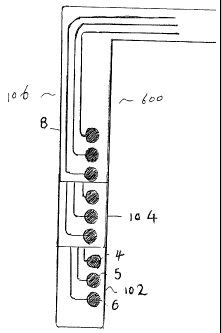
Fig. 6 shows a planar view of an implantable medical assembly with multiple
layers,
3o each having one or more conduction wires continuous with their
corresponding
electrodes according the present invention.
12
CA 02657522 2009-01-13
WO 2008/011721 PCT/CA2007/001333
Two or more implantable assembly layers 102, 104, and 106 are stacked in an
offset
fashion, thereby allowing all of the electrodes to be exposed. Each layer 102,
104, and
106 composing the electrode and conductors has the same width and thickness,
but may
or may not have the same length. The layers are aligned on top of each other
and are
superposed in a stepped shape. This stacking process can eliminate slow and
expensive
manufacturing process such as a folding process discussed above. The
implantable
assembly layers 102, 104, and 106 can be consolidated using heat and pressure.
io The separate implantable assembly layers 102, 104 and 106 can then be
melted
and conglomerated into a single assembly. Also the separate assembly layers
may be adhered together by using medical grade adhesive between each
assembly layer.
The implantable assembly layers 102, 104, and 106 shown in Fig. 6 are
conglomerated
into a single continuous film, having no boundaries between layers, by heat
treatment. Preferably, a layer of silicone can be over molded to form a
constrained
shape. This silicone layer can be added to part of the assembly structure or
molded over
the whole assembly.
Fig. 7 shows a perspective view of the implantable medical assembly with
multiple
layers having an overall corrugated shape according to the present invention.
This
assembly 700 may be applied to a cochlear implant or other nerve stimulating
implant,
wherein an extensible cable or lead is required. Further, this assembly 700
may be
used as a connection cable to the electronics housing containing the
stimulation
source, or as a connection cable between two electronics housings. To increase
the
expandability and elasticity of the implantable medical assembly 700, after a
predetermined stacking process, the implantable medical assembly or a portion
thereof
is molded to have the corrugated shape as shown in Fig. 7. Therefore, the
implantable
medical assembly 700 can readily be expanded or contracted.
13
CA 02657522 2009-01-13
WO 2008/011721 PCT/CA2007/001333
Fig. 8A shows a perspective view of the implantable medical assembly having an
overall corrugated shape encased with elastomer such as silicone according to
the
present invention. The implantable medical assembly 800 is encased with a
biocompatible elastomer 108 such as silicone to protect the overall
implantable
medical assembly 800 and to facilitate ease of handling of the assembly during
implantation according to the present invention. The cross sectional
configuration of
the silicone encapsulant may be circular, square, rectangular or any
appropriate shape
as dictated by the application of the device.
io Fig. 8B shows a side view of an alternative embodiment of the assembly in
which an
elastomer 108' such as silicone is embedded onto the underside of electrode
portion of
the assembly to enhance the implantability of the assembly.
Fig. 9A shows a perspective view of the implantable medical assembly having a
is terminal end which can be connected to a test device or stimulation source
(not
shown). As shown in Fig. 9A, this end terminal 120 will be easily connected to
a test
device or stimulation source (not shown) according to the number of channels
or its
application. The terminal 120 can be made of the same material used for the
rest of
the assembly including the electrodes and the conduction wires. Implantable
2o neurostimulation devices comprise an electronic control device coupled with
an
electrode array/cable system that conducts current to the target site. The
electrode
array/cable systems are normally constructed of one or more conductor wires
which,
at one end are located the stimulating electrodes (the electrode array) and at
the other,
a connection element for electrical connection to the electronic control
device. An
25 elastomer such as silicone 130 is preferably used to support and protect
the lead,
including the cable and connection elements, as shown in Fig. 9A.
Fig. 9B shows a perspective view of the implantable medical assembly having
double-
sided terminal ends which can be connected to a test device or stimulation
source (not
30 shown). If a double-sided connection portion is required, the end portions
of layer can
be wrapped around a layer of silicon elastomer 130 having a certain radius to
14
CA 02657522 2009-01-13
WO 2008/011721 PCT/CA2007/001333
minimize conduction circuit breaks. Then, this portion can be constrained with
silicone 130.
The present invention may be applied to the electrical connection (lead or
cable)
between implantable housings or medical devices in which electronic circuits
reside.
That is, in any implantable medical device designed to deliver or receive
electrical
signals, the present invention ensures safe and reliable delivery or receipt
of those
electrical signals. Further, this implantable medical assembly can be applied
to the
electrical connection between an implantable housing and an implantable
antenna for
io RF communication used in an implantable medical device.
Moreover, as described above, it is seen that the implantable medical assembly
described herein may be manufactured using low cost technology and simple-to-
implement manufacturing techniques for mass production.
Finally, it is seen that the implantable medical assembly of the present
invention may
be safely and reliably used in various nerve stimulation assemblies.
The above descriptions are intended to illustrate the preferred and
alternative
2o embodiments of the invention. It will be appreciated that modifications and
adaptations to such embodiments may be practiced without departing from the
scope
of the invention, such scope being most properly defined by reference to this
specification as a whole and to the following claims.