Note: Descriptions are shown in the official language in which they were submitted.
CA 02657840 2009-01-14
WO 2008/008755 PCT/US2007/073124
BI-PLANAR ELECTRODE WITH SHUNTING GATES
TECHNICAL FIELD
The present invention relates to electrodes for neural stimulation and, more
particularly, to
such electrodes disposed on opposite sides of a carrier.
BACKGROUND ART
Electrical stimulation of neural tissue is used for several purposes,
including pain control,
diagnosis and neural rehabilitation. For example, a cochlear implant (CI) is a
small electronic
device, part of which is placed under the skin, behind the ear, of a
profoundly deaf or severely hard
of hearing person. The cochlear implant receives signals from a microphone and
electrically
stimulates auditory nerves of the wearer. Although hearing through a CI may be
different than
normal hearing, the wearer perceives sounds and another person can orally
communicate with the
wearer.
CI and other neural stimulation is accomplished by placing at least one
electrode near
neural tissue and sending an electrical signal to the electrode. The
electrical signal is produced with
reference to a second (ground) electrode. That is, the signal is delivered
across the two electrodes.
The second electrode may be placed near the neural tissue or some distance
from the neural tissue.
The neural tissue is typically stimulated with a bi-phasic pulse, i.e., first
a positive pulse is sent to
the electrode, followed almost immediately thereafter by a negative pulse.
Better results are obtained from better focused electrical stimulation. Neural
tissues are
typically very small. To achieve desired results, selected individual nerves
should be stimulated.
However, prior art neural stimulation apparatus is unable to deliver well-
focused electrical
stimulation to neural tissue.
A conventional longitudinal bipolar neural stimulation scheme includes two
conducting
electrodes arranged side-by-side on an insulated carrier. A signal is fed to a
first of the two
electrodes, and the other electrode acts as a ground. During the positive
phase of the stimulation
signal, current flows from one of the electrodes, through the stimulated
tissue, into the other
(ground) electrode. During the negative phase of the stimulation signal, the
current flows in the
opposite direction, i.e., out of the ground electrode, through the stimulated
tissue, and into the first
CA 02657840 2009-01-14
WO 2008/008755 PCT/US2007/073124
electrode. Consequently, each of the electrodes acts as a stimulation point,
and the stimulation is not
well focused.
A conventional longitudinal tripolar scheme includes two ground electrodes
flanking a
center electrode. In this case, the amount of current that flows through each
of the two flanking
electrodes is one-half the amount of current that flows through the center
electrode. Tripolar
schemes produce reasonably well focused stimulation, however they require
three electrodes.
SUMMARY OF THE INVENTION
An embodiment of the present invention provides a neural stimulator that
includes a
nonconductive carrier. The carrier has a first side and a second side
substantially opposite the first
side. At least one first electrode is disposed on the first side of the
carrier, and at least one second
electrode disposed on the second side of the carrier. The at least one first
electrode is not
electrically connected to the at least one second electrode.
The carrier may have a circular, oval, rectangular or other cross-sectional
shape.
Each of the at least one first electrode may correspond to one of the at least
one second
electrode. In this case, each of the at least one second electrode may be
centered on a line that
perpendicularly bisects the corresponding first electrode. Alternatively, each
of the at least one
second electrode may be not centered on a line that perpendicularly bisects
the corresponding first
electrode
The neural stimulator may also include a signal source connected to one of the
at least one
first electrode and to the corresponding second electrode.
The carrier may include at least one shunt gate therethrough. In this case,
each shunt gate
defines a low-impedance electrical path through the carrier. Some or all of
the at least one shunt
gate may define a bore through the carrier. Optionally or alternatively, some
or all of the at least
one shunt gate may include an electrically conductive material.
Some or all of the second electrode may include a ring electrode. Some or all
of the ring
electrode may be formed by a photolithographic process. Optionally or
alternatively, some or all of
the ring electrode may be formed by a electrodeposition process. Optionally or
alternatively, some
or all of the ring electrode may be formed by a laser ablation deposition
process.
The at least one first electrode may include a plurality of electrodes
arranged in an array. In
this case, the at least one second electrode may include a plurality of
electrodes, each of the
plurality of electrodes including a ring electrode.
-2-
CA 02657840 2009-01-14
WO 2008/008755 PCT/US2007/073124
The carrier may include at least one shunt gate proximate each first
electrode. In this case,
each shunt gate defines a low-impedance electrical path through the carrier.
Optionally, each of the at least one first electrode includes at least one ear
disposed below a
surface of the carrier.
Optionally, the at least one first electrode includes a plurality of first
electrodes in a region
of the first side of the carrier. The region includes space between the
plurality of first electrodes.
The at least one second electrode includes an electrically conductive surface
on the second side of
the carrier. The surface has an area at least as large as the region on the
first side of the carrier.
BRIEF DESCRIPTION OF THE DRAWINGS
The invention will be more fully understood by referring to the following
Detailed
Description of Specific Embodiments in conjunction with the Drawings, of
which:
Fig. 1 is cross-sectional and top view of a neural stimulator, according to
the prior art;
Fig. 2 is cross-sectional and top view of another neural stimulator, according
to the prior art;
Fig. 3 is cross-sectional and top view of yet another neural stimulator,
according to the prior
art;
Fig. 4 is cross-sectional and top view of a neural stimulator, according to
one embodiment
of the present invention;
Fig. 5 is cross-sectional view of a neural stimulator, according to another
embodiment of
the present invention;
Fig. 6 is a top view of the neural stimulator of Fig. 5;
Fig. 7 is a top view of several exemplary shapes and arrangements of shunt
gates, according
to several embodiments of the present invention;
Fig. 8 is a top view of a neural stimulator, according to yet another
embodiment of the
present invention;
Fig. 9 is a bottom view of the neural stimulator of Fig. 8;
Fig. 10 is a close-up view of a ring electrode, according to one embodiment of
the present
invention;
Fig. 11 is a close-up view of a portion of a neural stimulator, according to
one embodiment
of the present invention;
Fig. 12 is a close-up top view and two sectional views of electrode ears,
according to one
embodiment of the present invention;
-3-
CA 02657840 2009-01-14
WO 2008/008755 PCT/US2007/073124
Fig. 13 is a cross-sectional view of a portion of a neural stimulator,
according to one
embodiment of the present invention; and
Fig. 14 is a cross-sectional view of a portion of a neural stimulator,
according to another
embodiment of the present invention.
DETAILED DESCRIPTION OF SPECIFIC EMBODIMENTS
In accordance with the present invention, methods and apparatus are disclosed
for
electrically stimulating neural tissue with focused stimulation signals. In
one embodiment, one or
more pairs of electrodes are disposed on an insulated carrier, such that one
of each pair of the
electrodes is disposed on one side of the carrier, and the other of the pair
of electrodes is disposed
on an opposite side of the carrier. An electrical stimulation signal is
delivered across the pair of
electrodes. Other embodiments, alternatives and options are described below,
following a brief
discussion of the prior art.
Fig. 1 is a section and top view of a conventional longitudinal bipolar neural
stimulator 100.
The stimulator 100 includes an electrically nonconductive carrier 102 and two
electrically
conductive electrodes 104 and 106 disposed on the carrier 102. The electrodes
104 and 106 are fed,
via conductive leads (not shown), by a signal source (not shown). For example,
during one phase of
biphasic stimulation, one of the electrodes 104 may be fed with a positive
pulse (as indicated by the
plus sign), and the other electrode 106 may form a return path (as indicated
by the minus sign) for
the stimulation signal.
Arrows 108 and 110 indicate the general direction of current (I) flow. During
another phase,
the current flows are reversed. Consequently, neural tissue 112 is stimulated
from two locations,
namely electrodes 104 and 106, and the stimulation is not well focused. The
amount of current (I)
flowing through one of the electrodes 104 into or out of tissue adjacent the
electrode 104 is equal to
the amount of current (I) flowing through the other electrode 106 out of or
into tissue adjacent the
other electrode 106. In other words, equal currents flow through the two
electrodes 104 and 106.
Fig. 2 is a section and top view of a conventional longitudinal tripolar
neural stimulator 200.
The stimulator 200 includes three electrodes 202, 204 and 206 on a
nonconductive carrier 208. Two
of the electrodes 204 and 206 are electrically connected together, such as by
a lead 210. The current
that flows through the center electrode 202 is designated I. One-half of this
current (i.e., 1/2) flows
through each of the two outer electrodes 204 and 206. Again, the stimulation
is not well focused.
Fig. 3 is a section view of yet another conventional neural stimulator 300.
The stimulator
300 includes a nonconductive carrier 302 and two electrodes 304 and 306. The
two electrodes 304
-4-
CA 02657840 2009-01-14
WO 2008/008755 PCT/US2007/073124
and 306 are electrically connected together, such as by a lead 308.
Consequently, half the
stimulation current (1/2) flows through each of the two electrodes 304 and
306. The stimulation
signal is provided with reference to a distant ground electrode (not shown).
As with the other prior-
art neural stimulators, the stimulation is not well focused.
Virtual Quadtrupolar Neural Stimulator
Fig. 4 is a section view of a neural stimulator 400, according to one
embodiment of the
present invention. The stimulator 400 includes a nonconductive carrier 402 and
two conductive
electrodes 404 and 406 disposed on opposite sides of the carrier 402. However,
unlike the prior art,
the two electrodes 404 and 406 are not electrically connected together.
Instead, the stimulating
signal is provided (via leads, not shown) to one of the electrodes 404 with
respect to the other
electrode 406. That is, the signal is provided across the electrodes 404 and
406. Thus, the same
amount of current (I) flows through each of the electrodes 404 and 406. Arrows
408 and 410
indicate current flow during a portion of the stimulation signal. During
another portion of the
stimulation signal the current flow may be reversed.
As shown in Section A-A, the carrier 402 can be round or oval in cross-
sectional shape.
Alternatively, as shown in Section A-A (Alternative), the carrier 402 can be
rectangular in cross-
sectional shape. In other embodiments (not shown), the carrier 402 can have
other cross-sectional
shapes. The thickness 412 of the carrier 402, i.e., the distance between the
two electrodes 404 and
406, along with the cross-sectional shape of the carrier 402 can be selected
to provide a stimulation
field having desired characteristics. For example, a larger distance between
the electrodes 404 and
406 requires a less powerful stimulation signal than a smaller separation
distance; however, a larger
separation often yields a less focused stimulation field.
As shown by the arrows in Section A-A and Section A-A (Alternative), one-half
the current
(i.e., 1/2) flows on each side of the carrier 402. Consequently, the neural
tissue 112 is stimulated
from a single point, i.e., the electrode 404 facing the neural tissue 112.
Typically, the stimulator 400
is positioned such that it is in a plane parallel to a plane of the neural
tissue 112. Thus, the
stimulating electrode 404 is in the parallel plane. The other electrode 406 is
also in a plane parallel
to the neural tissue 112, but the other electrode's 406 plane is located on
the opposite side of the
stimulating electrode 404. The plane of the other electrode 406 is referred to
herein as "antineural,"
i.e., on the opposite side from the plane of the stimulating electrode 404. I
have discovered that
disposing the return electrode 406 antineural focuses the stimulating signal.
As viewed from the neural tissue 112, and as seen in section B-B, the neural
stimulator 400
can have any shape, such as round or rectangular.
-5-
CA 02657840 2009-01-14
WO 2008/008755 PCT/US2007/073124
The electrodes 404 and 406 and leads (not shown) can be fabricated using
conventional
photolithographic, electrodeposition, pulsed laser ablation deposition or
other techniques. For
example, platinum can be deposited on a conventional carrier.
Shunt Gates
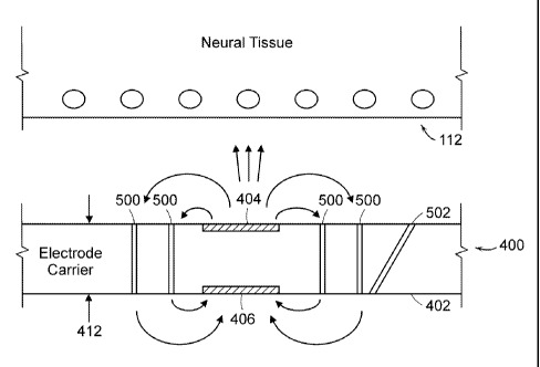
Optionally, as shown in Figs. 5 and 6, "shunt gates" 500 are included in the
carrier 402 of
the neural stimulator 400. (Fig. 6 is a top view of the neural stimulator
400.) The shunt gates 500
provide conductive or low-impedance paths through the carrier 402 for at least
some of the
stimulation signal. Thus, at least some of the current from the electrode 404
flows through the shunt
gates 500 to the other electrode 406, rather than flowing all the way around
the carrier 402. I have
discovered that, in some circumstances, the shunt gates 500 provide improved
focus of the
stimulation signal.
The shunt gates 500 can be open passages, holes, grooves, slots or other
openings
(collectively herein referred to as "bores") formed through or on the carrier
402. In this case,
conductive body fluid or tissue fills the shunt gates 500. Alternatively, the
carrier 402 can be made
with shunt gates 500 formed of an electrically conductive or low impedance
(collectively herein
referred to as "low-impedance") material, such as electrodeposited platinum
columns or a
conductive polymer, such as polypyrrole. Optionally, some of the shunt gates
500 are open
passages and others are low impedance material in the carrier 402.
The electrical resistance (R) of the shunt gates 500 is calculated according
to the equation:
R=(RoL)/A
where Ro is the resistivity of the bodily fluid or tissue in the bores or the
resistivity of the low-
impedance material in the shunt gates 500; L is the length of each shunt gate
500 (typically, the
thickness 412 of the carrier 402); and A is the cross-sectional or surface
area of the shunt gates 500.
A low resistance (R) can be achieved by using a large area (A) and/or a small
length (L).
Although the shunt gates 500 shown in Fig. 6 are straight, narrow slots
arranged in a
symmetric, rectilinear fashion, other shunt gate shapes,
symmetries/asymmetries and arrangements
may be used. Fig. 7 illustrates other exemplary, but non-limiting, shapes,
symmetries/asymmetries
and arrangements.
In addition, the shunt gates need not be perpendicular to the surface of the
carrier. For
example, as shown in Fig. 5, a shunt gate 502 can be formed at an angle other
than 90 to the
surface of the carrier 402.
Furthermore, the distances between the shunt gates 500 and the stimulating
electrode 404
can be varied. That is, not all the shunt gate 500 need be disposed the same
distance from the
-6-
CA 02657840 2009-01-14
WO 2008/008755 PCT/US2007/073124
stimulating electrode 404. The number, shape(s), arrangement, angle(s) and
placement(s) (relative
to the stimulating electrode 402) of the shunt gates 500 can be selected to
shape and orient the
stimulation field, as desired. For example, the distance between the
stimulating electrode 404 and
the shunt gates 500 can be selected to generate a stimulation field having a
desired shape and/or
orientation. Alternatively or in addition, the shunt gates 500 can be
positioned symmetrically or
asymmetrically around the stimulating electrode 404. The thickness 412 of the
carrier can be
selected to achieve a desired path length between the stimulating electrode
412 and the return
electrode 406. As long as the path length is relatively low, the stimulation
field may be affected by
the other geometric parameters described above.
Array of Stimulating Electrodes
The above-described neural stimulator 400 includes one stimulating electrode
404 and one
return electrode 406. However, in other embodiments, exemplified by a neural
stimulator 800
shown in Fig. 8, several stimulating electrodes 802 are disposed on a single
nonconductive carrier
804. For example, for spinal cord stimulation, the neural stimulator 800 may
contain hundreds of
stimulating electrodes 802 on a carrier that may be about 1 cm by 3 cm. Other
numbers of
stimulating electrodes 802 and other dimensions may be used.
Typically, although not necessarily, each of the electrodes 802 is connected
by a separate
lead (not shown) to a signal source (not shown). In some embodiments, each
electrode 802 has its
own signal source. Optionally, a switching matrix or other circuit (not shown)
is connected between
one or more signal sources and the electrodes 802 to select which electrode(s)
802 is provided with
a stimulating signal at a given time and, optionally, which signal source is
connected to the
electrode(s) 802. Thus, each of the electrodes 802 can be separately supplied
with a stimulation
signal, or not supplied with any signal. Consequently, as may be the case in a
CI, individual areas
of neural tissue can be stimulated by individual electrodes 802 or groups of
electrodes 802.
Optionally, groups of the electrodes 802 can be electrically connected
together and, thus, receive a
common stimulation signal.
In some embodiments, each of the stimulating electrodes 802 has a
corresponding return
electrode (not visible in Fig. 8) disposed on the opposite side of the carrier
804. These return
electrodes can each have an associated lead in the carrier 804 to provide a
return path to the signal
source. The return electrodes can, but need not, have the same size and shape
as the corresponding
stimulating electrodes 802. Alternatively, the return electrodes can be larger
or smaller than the
corresponding stimulating electrodes 802. Similarly, the return electrodes can
have different shapes
than the stimulating electrodes 802.
-7-
CA 02657840 2009-01-14
WO 2008/008755 PCT/US2007/073124
In some embodiments, each return electrode is centered on a line that extends
perpendicularly through the center of the corresponding stimulating electrode
802. In other
embodiments, the return electrodes are not co-centered with their
corresponding stimulating
electrodes 802. In yet other embodiments, a switching matrix or other circuit
is used to change,
from time to time, which return electrode corresponds to a given stimulating
electrode 802.
Ring Electrode
In one embodiment, each return electrode is a conductive ring 900, as shown in
Fig. 9. (Fig.
9 is a bottom view of the neural stimulator 800 of Fig. 8.) Alternatively, the
return electrodes 900
can be made in other solid or open shapes, such as polygons. Open-shape
polygonal return
electrodes are referred to herein as "rings," regardless of their shape.
Each return electrode 900 is preferably centered on its corresponding
stimulating electrode
802. Alternatively, as discussed above, the return electrodes need not be
centered on their
corresponding stimulating electrodes. Optionally, as discussed above, a
switching matrix or other
circuit is used to change, from time to time, which return electrode 900
corresponds to a given
stimulating electrode.
Preferably, the total conducting surface area of each ring 900 that is exposed
to tissue is
approximately equal to the total conducting surface area of the corresponding
stimulating electrode
802 that is exposed to tissue. The return electrodes 900 may be fabricated on
the carrier 804 using
photolithographic, electrodeposition, pulsed laser ablation deposition or
other techniques.
In one embodiment, a single ring electrode 900 of which is shown in Fig. 10,
each
stimulating electrode 802 is about 300 in diameter, and each ring electrode
900 has an inside
diameter 1000 of about 600 . (In Fig. 10, the stimulating electrode 802 is
shown using a dashed
line to indicate the stimulating electrode 802 is hidden, i.e., not visible
from the bottom of the
carrier 804.) The width 1002 of each ring electrode 900 can be calculated,
based on the diameter of
the stimulating electrode 802 and the diameter 1000 of the ring 900, such that
the two electrodes
have approximately equal surface areas, as discussed above. In general, the
width 1002 of the ring
electrode 802 is significantly less than the diameter of the stimulating
electrode 802. For example,
the diameters of the ring 900 and the stimulating electrode 802 may be related
as follows:
Dout - Din> D
where Doõt is the outside diameter of the ring 900; Diõ is the inside diameter
1000 of the ring 900;
and D is the diameter of the stimulating electrode 802.
In other embodiments, other sizes of stimulating electrodes 802 and/or other
sizes of ring
electrodes 900 can be used. For example, stimulating electrodes smaller than
about 300 in
-8-
CA 02657840 2009-01-14
WO 2008/008755 PCT/US2007/073124
diameter may be used, and ring electrodes 900 having inside diameters 1000 of
about 1 or 2 mm
can be used.
Alternatively, groups of the return electrodes 900 can be electrically
connected together to
provide a common ground return electrode for a group of the stimulating
electrodes 802. In one
embodiment, a single conductive plane is used instead of individual return
electrodes 900.
In yet another embodiment, a portion of which is shown in Fig. 11, a carrier
1100 includes
shunt gates 1102 between the ring electrodes 900 and the stimulating
electrodes 802. Optionally or
alternatively, the carrier 1100 includes shunt gates 1104 outside the ring
electrodes 900. As
discussed above, the shunt gates 1102 and 1104 can be any shape or size and
have any orientation,
relative to the stimulating electrodes 802 and the ring electrodes 900. Also,
as noted above, some or
all the ring electrodes 900 can be electrically connected together. In another
embodiment, the
bottom of the carrier 1100 is largely covered by a single conductive return
electrode, perforated by
the shunt gates 1102 and/or 1104.
Electrode Anchors
As noted, the electrodes are made of conductive material held in a non-
conductive carrier.
Depending on the materials used and the sizes of the electrodes, some
electrodes may include
anchors or ears to secure the electrodes to the carrier. As shown in Fig. 12,
in one embodiment, a
carrier 1200 includes an electrode 1202. Preferably, the surface 1204 of the
electrode 1202 is co-
planar with the surface 1206 of the carrier 1200, although the surface 1204 of
the electrode 1202
can be proud of, or depressed below, the surface 1206 of the carrier 1200.
Anchors (ears) 1208 are
formed on the electrode 1202 and beneath the surface 1206 of the carrier 1200
to secure the
electrode 1202 to the carrier 1200. A lead 1210 connected to the electrode
1202 also secures the
electrode 1202 to the carrier 1200. Similar anchors (ears) can be formed on
ring (or other shape)
electrodes (not shown) to secure the ring electrodes to the carrier 1200.
Stimulation Patterns
In an array of one or more stimulating electrodes and one or more return
electrodes
disposed on opposite sides of a nonconductive carrier, it is possible to
generate stimulation fields
having various patterns, depending on the number of electrodes and to which
pair of stimulating
and return electrodes a stimulating signal is sent. For example, as shown in
Fig. 13, a carrier 1300
can include four electrodes 1, 2, 3 and 4, any pair of which can be connected
to a signal source (not
shown). Each of the electrodes 1, 2, 3 and 4 has a lead (not shown), via which
the electrode can be
-9-
CA 02657840 2009-01-14
WO 2008/008755 PCT/US2007/073124
connected to the signal source, such as through a switching matrix or other
circuit (not shown).
Table 1 lists the possible combinations of electrodes that can be connected to
the signal source.
Table 1
Combinations of Electrodes Connected to a Signal Source
Electrode(s) Stimulation Pattern Comments
1(and a distant ground) Monopolar Prior art
2 (and a distant ground) Monopolar Prior art
3 (and a distant ground) Monopolar Prior art
4 (and a distant ground) Monopolar Prior art
1 and 4 Virtual Radial Quadrupolar New
2 and 3 Virtual Radial Quadrupolar New
1 and 2 Longitudinal Bipolar Prior art
3 and 4 Longitudinal Bipolar Prior art
1 and 3 Angled Bipolar New
2 and 4 Angled Bipolar New
As noted in Table 1, connecting a signal source to one of the electrodes 1, 2,
3 or 4 and to a
distant ground electrode is conventional. (The "distant ground" referred to in
Table 1 is not shown
in the drawings.) Similarly, using two adjacent electrodes on the same side of
a carrier, e.g.,
electrodes 1 and 2 or electrodes 3 and 4, is conventional.
However, as described above, connecting a signal source to two electrodes on
opposite
sides of the carrier, e.g., electrodes 1 and 4 or electrodes 2 and 3, is novel
and provides a better
focused stimulation field than in the prior art.
Furthermore, using a return electrode that is not directly behind a
stimulating electrode, e.g.,
using electrodes 1 and 3 or electrodes 2 and 4, creates a stimulation field
that is directed "off-axis,"
i.e., not along an axis that perpendicularly bisects the stimulating
electrode. In this regard, using a
carrier that includes more than two return electrodes in the antineural plane,
as shown in Fig. 14,
and pairing a particular stimulating electrode, such as electrode 2, with one
or more of the return
electrodes 3-7, the stimulation field can be steered toward selected portions
of the neural tissue 112.
This steering can provide more spatial resolution than simply selecting a
different pair of electrodes
that are positioned directly opposite each other on the carrier. Furthermore,
the return electrodes 3-7
-10-
CA 02657840 2009-01-14
WO 2008/008755 PCT/US2007/073124
need not be positioned directly opposite the stimulating electrodes, and the
carrier can have more or
fewer return electrodes than stimulating electrodes.
Although the neural stimulators shown in Figs. 13 and 14 include a small
number of
electrodes, these drawings can alternatively be interpreted to represent only
a portion of a neural
stimulator that includes many more electrodes (not shown). In addition, the
above-described shunt
gates can be combined with angled bipolar stimulation. Other combinations of
the features
described herein are also possible.
While the invention is described through the above-described exemplary
embodiments, it
will be understood by those of ordinary skill in the art that modifications
to, and variations of, the
illustrated embodiments may be made without departing from the inventive
concepts disclosed
herein. Moreover, while some embodiments are described in connection with
various illustrative
materials and fabrication techniques, one skilled in the art will recognize
that the system may be
embodied using a variety of other materials or fabrication techniques.
Similarly, while some
embodiments can be used in cochlear implants (CI), these and other embodiments
can be used for
other types of neural stimulation, such as cortical, spinal or bladder
stimulation, for pain control,
diagnosis, neural rehabilitation and other purposes. Accordingly, the
invention should not be
viewed as limited, except by the scope and spirit of the appended claims.
-11-