Note: Descriptions are shown in the official language in which they were submitted.
CA 02658092 2009-01-16
WO 2008/011061 PCT/US2007/016276
CCIO005WO
METHOD AND APPARATUS FOR SOLID-STATE MICROBATTERY
PHOTOLITHOGRAPHIC MANUFACTURE, SINGULATION AND
PASSIVATION
This application claims the benefit of U.S. Provisional Application Serial
No. 60/807,713, filed July 18, 2006, entitled "METHOD AND APPARATUS FOR
SOLID-STATE MICROBATTERY PHOTOLITHOGRAPHIC SINGULATION
AND PASSIVATION FROM A SUBSTRATE" which application is incorporated
herein by reference in its entirety.
1o FIELD OF THE INVENTION
This invention relates to the field of solid-state energy-storage devices, and
more specifically to a method and apparatus for making solid-state batteries
and
singulating the devices (mostly separating from each other while optionally
leaving
small connections to the surrounding waste substrate, or completely separating
the
devices) and creating passivation around the battery devices, e.g., lithium
battery
devices with a LiPON electrolyte, wherein the battery devices also optionally
include LiPON as a passivation and protective barrier, and the resulting
cell(s),
device(s) and/or battery(s).
BACKGROUND OF THE INVENTION
Electronics have been incorporated into many portable devices such as
computers, mobile phones, tracking systems, scanners, etc. One drawback to
portable devices is the need to include the power supply with the device.
Portable
devices typically use batteries as power supplies. Batteries must have
sufficient
capacity to power the device for at least the length of time the device is in
use.
Sufficient battery capacity can result in a power supply that is quite heavy
and/or
large compared to the rest of the device. Accordingly, smaller and lighter
batteries
(i.e., power supplies) with sufficient energy storage are desired. Other
energy
storage devices, such as supercapacitors, and energy conversion devices, such
as
photovoltaics and fuel cells, are alternatives to batteries for use as power
supplies in
portable electronics and non-portable electrical applications.
Another drawback of conventional batteries is the fact that some are
fabricated from potentially toxic materials that may leak and be subject to
CA 02658092 2009-01-16
WO 2008/011061 PCT/US2007/016276
2
govemmental regulation. Accordingly, it is desired to provide an electrical
power
source that is safe, solid-state and rechargeable over many charge/discharge
life
cycles.
One type of an energy-storage device is a solid-state, thin-film battery.
Examples of thin-film batteries are described in U.S. Patent Nos. 5,314,765;
5,338,625; 5,445,906; 5,512,147; 5,561,004; 5,567,210; 5,569,520; 5,597,660;
5,612,152; 5,654,084; and 5,705,293, each of which is herein incorporated by
reference. U.S. Patent No. 5,338,625 describes a thin-film battery, especially
a thin-
film microbattery, and a method for making same having application as a backup
or
first integrated power source for"electronic devices. U.S. Patent No.
5,445,906
describes a method and system for manufacturing a thin-film battery structure
formed with the method that utilizes a plurality of deposition stations at
which thin
battery component films are built up in sequence upon a web-like substrate as
the
substrate is automatically moved through the stations.
U.S. Patent 6,805,998 (which is iricorporated herein by reference) issued
October 19, 2004, by Mark L. Jenson and Jody J. Klaassen, and is assigned to
the
assignee of the present invention described a high-speed low-temperature
method
for depositing thin-film lithium batteries onto a polymer web moving through a
series of deposition stations.
U.S. Patent Application 10/895,445 entitled "LITHIUM/AIR BATTERIES
WITH LIPON AS SEPARATOR AND PROTECTIVE BARRIER AND
METHOD" (which is incorporated herein by reference) describes a method for
making lithium batteries including depositing LiPON on a conductive substrate
(e.g., a metal such as copper or aluminum) by depositing a chromium adhesion
layer
on an electrically insulating layer of silicon oxide by vacuum sputter
deposition of
500A of chromium followed by 5000A of copper. In some embodiments, a thin film
of LiPON (Lithium Phosphorous OxyNitride) is then formed by low-pressure (<10
mtorr) sputter deposition of lithium orthophosphate (Li3PO4) in nitrogen. In
some
embodiments of the Li-air battery cells, LiPON was deposited over the copper
anode
contact to a thickness of 2.5 microns, and a layer of lithium metal was formed
onto
the copper anode contact by electroplating though the LiPON layer in a
propylene
carbonate/LiPF6 electrolyte solution. In some embodiments, the air cathode was
a
CA 02658092 2009-01-16
WO 2008/011061 PCT/US2007/016276
3
carbon powder/ polyfluoroacrylate-binder coating (Novec- 1700) saturated with
a
propylene carbonate/LiPF6 organic electrolyte solution. In other embodiments,
a
cathode-contact layer having carbon granules is deposited, such that
atmospheric
oxygen could operate as the cathode reactant. This configuration requires
providing
air access to substantially the entire cathode surface, limiting the ability
to densely
stack layers for higher electrical capacity (i.e., amp-hours).
US Patent Application Publication No. 20070067984 describes a method for
producing a lithium microbattery, wherein the electrolyte containing a
lithiated
compound is formed by successively depositing an electrolytic thin film, a
first
protective thin film that is chemically inert in relation to the lithium, and
a first
masking thin film on a substrate provided with current collectors and a
cathode. As
stated therein at paragraph [0033], "At the present time, the elements
constituting
the lithium microbattery containing lithiated compounds that are very
sensitive to
oxygen, nitrogen and water can not be formed with the techniques implemented
to
produce the current collectors 2a and 2b and the cathode 3 and in particular
by
photolithography and by etching."
There is a need for producing rechargeable lithium-based batteries with
improved manufacturability, density, and reliability, and lowered cost.
SUMMARY OF THE INVENTION
A method for producing a thin film lithium battery is provided, comprising
applying a cathode current collector, a cathode material, an anode current
collector,
and an electrolyte layer separating the cathode material from the anode
current
collector to a substrate, wherein at least one of the layers contains
lithiated
compounds. ln this method, the configuration of at least one of the layers
containing
lithiated compounds is patterned at least in part by a photolithography
operation
comprising removal of a photoresist material from the layer containing
lithiated
compounds by a process including a wet chemical treatment.
Contrary to the teachings of the prior art, it has been found that thin film
lithium batteries can be prepared using photolithographic operations using wet
chemical treatments. The methods as described herein provide efficient and
economical manufacturing of these devices with a reduced number of steps,
using
less complicated equipment as compared to prior art manufacturing techniques.
CA 02658092 2009-01-16
WO 2008/011061 PCT/US2007/016276
4
Thus, the present process for making thin film lithium batteiies can
preferably be
carried out without using extra protective layers in addition to
photolithographic
masking materials that can be removed using wet chemical treatments.
In another aspect, the present invention includes a method and apparatus for
making lithium batteries by providing a first sheet that includes a substrate
having a
cathode material, an anode current collector, an optional anode material, and
a
LiPON barrier/electrolyte layer separating the cathode material from the anode
current collector; and laser ablating or by performing one or more one or more
material removal operations on a subset of first material to separate a
plurality of
cells from the first sheet. In some embodiments, the method further includes
depositing second material on the sheet to cover the plurality of cells; and
perfonning one or more one or more material removal operations on a subset of
second material to separate a plurality of cells from the first sheet. The one
or more
material removal operations may be laser ablating or by performing one or more
photolithography operations, or a combination thereof.
BRIEF DESCRIPTION OF THE DRAWINGS
FIG. 1 A is a schematic cross-section view of a partially manufactured
layered structure 100A for making a solid-state cell of some embodiments of
the
invention.
FIG. 1 B is a schematic cross-section view of a layered structure I OOB for
making a solid-state cell of some embodiments of the invention.
FIG. 2A is a schematic cross-section view of an ablated layered structure
200A for making a solid-state cell of some embodiments of the invention.
FIG. 2B is a schematic cross-section view of an ablated layered structure
200B for
making a solid-state cell of some embodiments of the invention.
FIG. 3A is a schematic cross-section view of an ablated and filled solid-state-
cell-inprocess 300A of some embodiments of the invention.
FIG. 3B is a schematic cross-section view of an ablated and filled solid-state-
cell-inprocess 300B for making a solid-state of some embodiments of the
invention.
FIG. 4A is a schematic cross-section view of a re-ablated solid-state cell
400A of some embodiments of the invention.
CA 02658092 2009-01-16
WO 2008/011061 PCT/US2007/016276
FIG. 4B is a schematic cross-section view of a re-ablated solid-state cell
400B of some embodiments of the invention.
FIG. 5 is a schematic top-down view of a re-ablated solid-state cell 500 of
some embodiments of the invention.
5 FIG. 6 is a schematic cross-section view of a partially manufactured layered
structure 600 for making a solid-state cell of some embodiments of the
invention.
FIG. 7 is a schematic cross-section view of an ablated layered structure 700
for making a solid-state cell of some embodiments of the invention.
FIG. 8 is a schematic cross-section view of an ablated and filled solid-state-
cell-inprocess 800 of some embodiments of the invention. In some embodiments,
fill
material 810 is a metal such as copper or aluminum or the like.
FIG. 9 is a schematic cross-section view of a solid-state-cell-in-process 900
of some embodiments of the invention. In some embodiments, fill material 810
is
ablated in channels 812, leaving a thin layer of material 810. In some
embodiments,
the substrate is moved back into the laser ablation system or dicing saw for
contact
definition and cell separation. In some embodiments, the laser beam or dicing
saw
ablates the through the layers of passivation material to the contact on the
top of
each cell (Figure 9). Following the contact definition, the laser is set at a
percentage
(less than 100 percent) of the original ablation kerf width. The beam ablates
through
the passivation material and through the substrate with the exception of small
support tabs 1017 in the corners, and an opening center of each cell side
(Figure 10).
FIG. 10 is a schematic cross-section view of a solid-state-cell-in-process
1000 of some embodiments of the invention. In some embodiments, the cells
remain
in the substrate though post ablation operations. Final separation of the
cells is
accomplished by upward or downward force on individual cells through a pick
and
place system.
FIG. 1 l is a schematic cross-section view of a solid-state-cell-in-process
1100 of some embodiments of the invention after a blanket cell process. In
cells
where both contacts are accessed through the top of the cell; the process is
similar to
those described above with the exception of the ablation definition.
FIG. 12 is a schematic cross-section view of a solid-state-cell-in-process
1200 showing cell and top side contacts defined through ablation.
CA 02658092 2009-01-16
WO 2008/011061 PCT/US2007/016276
6
FIG. 13 is a schematic cross-section view of a solid-state-cell-in-process
1300 showing a first Iayer of passivation applied.
FIG. 14 is a schematic cross-section view of a solid-state-cell-in-process
1400 showing a first layer of passivation material is ablated to uniformly
cover the
cell.
F1G. 15 is a schematic cross-section view of a solid-state-cell-in-process
1500 showing additional layer(s) of passivation material is applied (metal).
FIG. 16 is a schematic cross-section view of a solid-state-cell-in-process
1600 showing contact areas of the cell are ablated and the cells are ablated
with the
exception of substrate support tabs.
FIG. 17 is a schematic top view of a solid-state-cell-in-process 1700 showing
a top view of cells with contact pads identified and support tabs identified.
FIG. 18 is a schematic cross-section view of a solid-state-cell 1800 prepared
by the present method.
is DESCRIPTION OF PREFERRED EMBODIMENTS
In the following detailed description of the preferred embodiments, reference
is made to the accompanying drawings that form a part hereof, and in which are
shown by way of illustration specific embodiments in which the invention may
be
practiced. It is understood that other embodiments may be utilized and
structural
changes may be made without departing from the scope of the present invention.
The leading digit(s) of reference numbers appearing in the Figures generally
correspond to the Figure number in which that component is first introduced,
such
that the same reference number is used throughout to refer to an identical
component
which appears in multiple Figures. Signals (such as, for example,
fluid'pressures,
fluid flows, or electrical signals that represent such pressures or flows),
pipes, tubing
or conduits that carry the fluids, wires or other conductors that carry the
electrical
signals, and connections may be referred to by the same reference number or
label,
and the actual meaning will be clear from its use in the context of the
description.
TERMINOLOGY
In this description, the term metal applies both to substantially pure single
metallic elements and to alloys or combinations of two or more elements, at
least
one of which is a metallic element.
CA 02658092 2009-01-16
WO 2008/011061 PCT/US2007/016276
7
The tenn substrate or core generally refers to the physical structure that is
the
basic work piece that is transfonmed by various process operations into the
desired
microelectronic configuration. In some embodiments, substrates include
conducting
material (such as copper, stainless steel, aluminum and the like), insulating
material
(such as sapphire, ceramic, or plastic/polymer insulators and the like),
semiconducting materials (such as silicon), nonsemiconducting, or combinations
of
semiconducting and non-semiconducting materials. In some other embodiments,
substrates include layered structures, such as a core sheet or piece of
material (such
as iron-nickel alloy and the like) chosen for its coefficient of thermal
expansion
(CTE) that more closely matches the CTE of an adjacent structure such as a
silicon
processor chip. In some such embodiments, such a substrate core is laminated
to a
sheet of material chosen for electrical and/or thermal conductivity (such as a
copper,
aluminum alloy and the like), which in turn is covered with a layer of plastic
chosen
for electrical insulation, stability, and embossing characteristics. An
electrolyte is a
material that conducts electricity by allowing movement of ions (e.g., lithium
ions
having a positive charge) while being non-conductive to electrons. An
electrical cell
or battery is a device having an anode and a cathode that are separated by an
electrolyte. A dielectric is a material that is non-conducting to electricity,
such as,
for example, plastic, ceramic, or glass. In some embodiments, a material such
as
LiPON can act as an electrolyte when a source and sink for lithium are
adjacent the
LiPON layer, and can also act as a dielectric when placed between two metal
layers
such as copper or aluminum, which do not form ions that can pass through the
LiPON. In some embodiments, devices include an insulating plastic/polymer
layer
(a dielectric) having wiring traces that carry signals and electrical power
- horizontally, and vias that carry signals and electrical power vertically
between
layers of traces.
The term vertical is defined to mean substantially perpendicular to the major
surface of a substrate. Height or depth refers to a distance in a direction
perpendicular to the major surface of a substrate.
The term "layer containing lithiated compounds" is defined to mean a layer
that contains lithium in any form, including metallic lithium,.alloys of
lithium and
lithium containing compounds. Examples of layers containing lithiated
compounds
CA 02658092 2009-01-16
WO 2008/011061 PCT/US2007/016276
8
include the anode, particularly in the case of metallic lithium, the
electrolyte,
particularly in the case of LiPON, and the cathode, particularly where the
cathode
layer is a material such as LiCoO2 that can act as a source of lithium ions.
As used
herein, LiPON refers generally to lithium phosphorus oxynitride materials. One
example is Li3PO4N. Other examples incorporate higher ratios of nitrogen in
order
to increase lithium ion mobility across the electrolyte.
As noted above, the present invention provides in one aspect a method for
producing a thin film lithium battery wherein the configuration of at least
one of the
layers containing lithiated compounds is pattemed at least in part by a
photolithography operation comprising removal of a photoresist material from
the
layer containing lithiated compounds by a process including a wet chemical
treatment.
In preferred embodiments, the layer containing lithiated compounds is a
cathode material or is an electrolyte. In an embodiment of the present
invention, the
thin film battery is initially constructed without an anode, but with a
cathode layer
that can act as a source of lithium ions. Upon charging of this thin film
battery
embodiment, metallic lithium is plated between the electrolyte and the anode
current
collector to form an anode.
It will be understood that in one aspect of the invention, the battery is
built in
layers as a "bottom up" construction, whereby the substrate is provided with a
cathode current collector, a cathode, a solid electrolyte, an anode (which is
optional
during the construction phase as discussed above), an anode current collector,
and
one or more encapsulant materials. Optionally, the cathode and anode may be
provided in a side by side or other configuration. Alternatively, the battery
may be
constructed in an "upside down" order, where the layers are formed in reverse
order
from that discussed above. Altematively, the layers may be formed separately
and
joined by a lamination process as will now be readily envisioned by the
routineer in
this art.
In a configuration of the present invention, the electrolyte overlays the
cathode, preferably with an overlay distance of from about 5 to about 20
microns per
edge. Configurations wherein the electrolyte underlays the cathode, preferably
with
CA 02658092 2009-01-16
WO 2008/011061 PCT/US2007/016276
9
an underlay distance of from about 5 to about 20 microns per edge, are
specifically
contemplated.
The photolithography operation of the present method preferably comprises
a) applying a photoresist material to the surface of at least one of the
layers
containing lithiated compounds,
b) processing the photoresist material to provide a pattern,
c) applying a developer to remove portions of the photoresist material,
thereby defining masked and unmasked portions of the layer containing
lithiated
compounds,
d) removing unmasked portions of the layer containing lithiated compounds,
and
e) removing the remaining photoresist material from the layer containing
lithiated compounds by a wet chemical treatment.
The photoresist in one embodiment is a positive tone photoresist, and in
another embodiment is a negative tone photoresist. Examples of such
photoresists
are well known in the art.
The wet chemical process used to remove the remaining photoresist material
from the layer containing lithiated compounds preferably is a non-aqueous
process.
Preferably, the wet chemical treatment comprises application of an organic
solvent,
such as N-Methylpyrrolidone. The wet chemical process may optionally be
augmented by application of plasma chemistries, such as plasma 02 chemistries.
In an aspect of the present invention, at least two of the process steps of
applying the cathode current collector, the cathode material, the anode
current
collector, and the electrolyte layer are carried out in different processing
apparatus.
It has surprisingly been found that during the production of the thin layer
lithium
battery, satisfactory batteries are obtained even if at least one layer
containing
lithiated compounds is exposed to ordinary air conditions between process
steps.
In an aspect of the present invention, it has been found that superior
performance of the battery is obtained when the patterning of the layer
containing
lithiated compounds by a photolithography operation is carried out within
about 72
hours of initial formation of the layer containing lithiated compounds.
Preferably,
the patterning of the layer containing lithiated compounds by a
photolithography
CA 02658092 2009-01-16
WO 2008/011061 PCT/US2007/016276
- ~v-
operation is carried out within about 48 hours, and more preferably within
about 30
hours, of initial formation of the layer containing lithiated compounds.
In one aspect, the invention provides a method and apparatus for defining the
boundaries of and separating individual battery cells from a larger sheet
having a
5 multilayered cathode-electrolyte anode structure manufactured on a large
substrate
of material (through the depositing of rnaterials on the surface of the
substrate in a
substantially uniform blanket process).
In some embodiments, the specification describes how the cells are defined,
passivated, and removed from the material. In some embodiments, the invention
10 uses laser ablation and/or dicing-saw techniques to remove the material for
trenches
used for defining single cells, coating the sides of the cells with
passivation material
(e.g., insulation and leveling material (material to level or flatten a
surface, so later
materials have better surface coverage) such as polymer, photoresist, LiPON,
or
other suitable materials, and/or metal layers used for electrical conductors
and/or
vapor and oxygen barriers). In other embodiments, (see the description of
Figure 18,
below) photolithographic techniques are used instead of laser ablation to mask
and
remove material, leaving the desired pattern of battery material, that is then
coated
with passivation and/or conductors. Further, techniques described for use with
the
laser ablation techniques are used in some embodiments of the
photolithographic
techniques, and vice versa.
Note that the schematic figures used herein are not to scale: the vertical
thicknesses of the thin-film batteries described are extremely thin (e.g.,
less than
about 10 microns, in some embodiments, and even less than 4 microns in other
embodiments) as compared to the device lateral widths (e.g., 1000 microns (=1
mm)
to 10,000 microns (=10 mm) in some embodiments, and up to several centimeters
in
other embodiments). Further, the trenches in some embodiments of the present
invention are about 10 microns or less wide. In particular, photolithographic
techniques allow trench widths and other dimensions to be very small and/or
very
accurate, as compared to shadow mask techniques.
In some embodiments, the battery cell devices of the present invention use
materials, processes, techniques of the various patents and patent
applications (e.g.,
U.S. Provisional Patent Application 60/700,425, U.S. Patent Application
CA 02658092 2009-01-16
WO 2008/011061 PCT/US2007/016276
11
10/895,445, U.S_ Patent Application 11/031,217 (entitled "LAYERED BARRIER
STRUCTURE HAVING ONE OR MORE DEFINABLE LAYERS AND
METHOD" filed January 6, 2005 by D. Tarnowski et al.), U.S. Patent Application
11/458,091 (entitled "THIN-FILM BATTERIES WITH SOFT AND HARD
ELECTROLYTE LAYERS AND METHOD" filed July 17, 2006 by J. Klaassen),
and U.S. Patent 6,805,998) that are incorporated herein by reference, and in
general
those are not further discussed here_
LASER-ABLATION AND/OR DICING-SAW TECHNIQUES
Figure l.A is a schematic cross-section view of a partially manufactured
layered structure I OOA (also called a "blanket") for making a plurality of
solid-state
cells (e.g., battery cells for storing electrical power) of some embodiments
of the
invention. In some embodiments, structure I OOA begins with a substrate I 10,
which,
in various embodiments, is a metal foil, or a silicon or sapphire wafer, or a
plastic
film such as, for example, Kapton"m (solid-state battery cells are fabricated
on a
carrier material referred to as substrate I 10). The substrate can include a
choice of
one or more materials including, for example, silicon, ceramic, metal foils
(both
ferrous, non-ferrous, and alloys), flexible polymers (e.g., KaptonTM,
polyethylene,
polypropylene, polycarbonate, etc.) and composites that include such polymers,
rigid
polymers and composites (i.e., printed-circuit-board (PCB) material). In some
embodiments, the substrate is provided in a selected sheet size or, in other
embodiments, as a continuous roll of material. In some embodiments, an
optional
insulating layer 112 (such as, for example, silicon nitride or oxidized
silicon (Si02))
is deposited on substrate 110, depending on the substrate used and whether
electrical
conductiori is desired through the bottom or sides of the substrate 110.
ln some embodiments, a multilayered vapor barrier (which also acts as an
insulating layer) is used for layer 112, such as described in U.S. Patent
Application
11/031,217 entitled "LAYERED BARRIER STRUCTURE HAVING ONE OR
MORE DEFINABLE LAYERS AND METHOD" filed January 6, 2005 by David
Tarnowski et al., which is incorporated herein in its entirety by reference.
In some embodiments, an adhesion layer 114 (e.g., a metal such as chrome or
titanium or other suitable adhesive material) is then deposited, and a cathode
contact
layer 116 (e.g., a metal such as copper, nickel or aluminum or suitable
conductive
CA 02658092 2009-01-16
WO 2008/011061 PCT/US2007/016276
12
materials, e.g., chosen so that it does not migrate into the cathode) is then
deposited.
Cathode material 118 (such as lithium cobalt oxide, LiCoO2) is then deposited,
and
is covered with one or more electrolyte layers 120 (such as LiPON and/or a
lithium-
conducting polymer electrolyte or other suitable electrolyte, for example, a
multilayered electrolyte such as described in U.S. Patent Application
11/458,091
entitled "THIN-FILM BATTERIES WITH SOFT AND HARD ELECTROLYTE
LAYERS AND METHOD." In some embodiments, an anode and/or anode contact
material (such as, for example, copper, nickel or aluminum and/or lithium
covered
by copper, nickel or aluminum) is deposited (in some embodiments, the anode-
contact material (e.g., copper or nickel) is deposited on LiPON electrolyte,
and the
lithium is later plated (e.g., by the first charging of the battery)). In some
embodiments, the cell is charged later by plating lithium through the
electrolyte 120
and onto anode contact material 122. In some embodiments, one or more
protective
or passivation layers 123 and/or 124 (or still further pairs of alternating
layers, e.g.,
of an insulating smoothing layer such as photoresist (e_g_, Shipley 220
photoresist;
various polyimides from HD Microsystems, such as the 2720 series, which
includes
2727, 2723, 2729; the 2770 series which includes 2770 and 2772; the 2730 which
includes 2731 and 2737; the PIX Series which includes PIX-1400, PIX-3476, PIX-
S200, PIX-6400; the 2500 series, which includes 2525, 2555, 2575 and 2556; and
various other polymeric materials such as Cyclotene product numbers 3022-35,
3022-46, 3022-57 and 3022-63 from Dow Chemical Company; photodefinable
silicones such as WL-5351 and WL-301 0 from Dow Chemical Company; and UV
curable epoxy such as 9001 from Dymax Corporation, or the like) and a metal
layer
such as aluminum or copper or the like). Each layer is deposited with the
appropriate
material at the required thickness to allow for the desired Cells energy
density. In
some cases, the substrate (e.g., if made of a conductor such as a metal foil
(e.g.,
copper foil) can serve as an electrical contact of the cell. In some
embodiments, the
positive portion (i.e., substrate 110, insulator 112, adhesion layer 11.6,
cathode
contact 116, cathode material 118, and one LiPON layer (a portion of
electrolyte
120)) is formed as a first sub-sheet, while anode contact layer 112 covered on
its
lower (relative to the Figure) surface by a LiPON layer (another portion of
electrolyte 120) as a second sub-sheet, and then the first and second sub-
sheets are
CA 02658092 2009-01-16
WO 2008/011061 PCT/US2007/016276
13
laminated together using a soft electrolyte layer (yet another portion of
electrolyte
120) therebetween. In some embodiments, the soft electrolyte layer includes
polyphosphazene and a lithium salt, or any suitable polymer layer (solid, gel,
or
liquid/sponge) such as described in U.S. Patent Application 11/458,091
entitled
"THIN-FILM BATTERIES WITH SOFT AND HARD ELECTROLYTE LAYERS
AND METHOD."
In some embodiments, substrate l 10 is about 500 microns (or thinner) to
about 1000 microns (or thicker) thick (e.g., 525 or 625 microns of silicon
wafer, in
some embodiments). In other embodiments, substrate I 10 includes a polymer
layer
(e.g., Kapton) that can be as thin as 25 microns or thinner. In some
embodiments,
layer 112 is about one micron of silicon nitride, layer 114 is about 0.5
microns of
titanium, layer 116 is about 0.5 microns of nickel, layer 118 is about 5 to 10
microns
of lithium_cobalt oxide, electrolyte layer 120 is about 1 to 2.5 microns of
LiPON,
and layer 122 is about 3 microns of copper. In some embodiments, additional
layers
are added on top (e.g., 10 microns of a polymer such as Shipley 220
photoresist,
then 7 microns of a metal such as copper or aluminum, then 10 more microns of
a
polymer such as Shipley 220 photoresist, then 3 to 7 more microns of a metal
such
as copper or aluminum).
Figure 1 B is a schematic cross-section view of a layered structure I OOB for
making a solid-state cell of some embodiments of the invention. In some
embodiments, layered structure 100B has similar reference-numbered layers as
described above for Figure lA. Note: The singulation process described here
can be
utilized for single- or multi-layer passivation processes. The ablation
process
(defined herein as removal of material by laser or other radiation ablation
(called
herein "laser ablation") and/or (sawing or scribing of a kerf) and/or
photoresist-
defined etching or dissolving) can be utilized to open contact areas to
underlying
features (metal contacts) in multiple configurations (even in different
configurations
on the same sheet) to provide different cell sizes or electrical contact
configurations,
and/or expose side walls that can be covered by one or more protective layers.
Subsequent layers of the battery cell device and/or other devices may then be
deposited (either as a blanket deposition (that can be patterned using
photoresist
techniques) or defined by shadow masks), and other patterns laser-ablated or
CA 02658092 2009-01-16
WO 2008/011061 PCT/US2007/016276
14
otherwise selectively removed, in a manner similar to semiconductor
processing. In
some embodiments, the laser ablation is accomplished to the desired depth less
than
completely through (or, in other embodiments, completely through the material)
using a series of shallower ablation-removal steps (e.g., multiple laser
ablation paths
left-to-right and top to bottom across the blanket are ablated multiple times,
each
time removing a shallow amount of additional material) in order to avoid
overheating or melting of surrounding areas. In some embodiments, the laser
ablation paths are followed in an interleaved pattern (e.g., on a first pass,
ablate to a
first depth the first one of every three adjacent vertical lines and the first
one of
every three adjacent horizontal vertical lines, on a second pass, ablate to
the first
depth the second one of every three adjacent vertical lines and the second one
of
every three adjacent horizontal vertical lines, and on a third pass, ablate to
the first
depth the first one of every third adjacent vertical lines and the first one
of every
third adjacent horizontal vertical lines, then repeat to ablate each line to a
second
(deeper) depth, and optionally ablate to even deeper depths on subsequent
rounds).
In some embodiments, the completed blanket or sheet or a portion of a rolled
section of cell material I OOA or 100B is located on a positioning table for
ablation
and/or cutting. In various embodiments, a laser, or a dry- or wet-wafer-dicing
saw is
programmed to singulate the appropriate size cell from the blanket of material
for
the ablation process. The area removed between the cells is called the kerf
(e.g.,
channel 211 or 212 described below).
In some embodiments, a cut is made part-way-through cell material 100A or
100B to separate individual cells from one another, while leaving a portion of
the
substrate uncut. In some embodiments, the substrate is cut and separated into
a
plurality of pieces, each piece having one or more cells. Then one or more
passivation layers are added to seal the now-exposed sides of the cells. In
some
embodiments, the cells are later singulated (completely separated) from one
another.
Figure 2A is a schematic cross-section view of an ablated layered structure
200A for making a solid-state cell of some embodiments of the invention. In
some
embodiments, a series of kerfs or channels are cut (e.g., using either a
single cut, or
by repeated shallower cuts), e.g., by laser ablation of the material. In some
embodiments, vertical-walled channels 211 are cut, such as shown in Figure 2A,
CA 02658092 2009-01-16
WO 2008/011061 PCT/US2007/016276
leaving a plurality of islands 210 of battery layers. In other embodiments,
sloping-
walled channels 212 are cut, such as shown in Figure 2B. In some embodiments,
each island is rectangular in shape, as viewed from above. In other
embodiments, the
islands are other selected shapes as desired. In some embodiments, a large
plurality
5 of islands are formed in both dimensions across the face of the sheet 100A.
Figure 2B is a schematic cross-section view of an ablated layered structure
200B for making a solid-state cell of some embodiments of the invention. In
some
embodiments,,sloping walled channels 212 are cut, in order that subsequent
deposited layers more fully cover the side walls. In some embodiments, a large
10 plurality of islands are formed in both dimensions across the face of the
sheet 100B.
In some embodiments, the ablation process includes removing the deposited
material through the vaporization or cutting of material at a precisely
controlled rate.
The laser or dicing saw is controlled in the z-axis (vertical in Figure 2A and
Figure
2B) for proper depth control, the kerf width is set to allow additional
material to be
is deposited. The controlled rate of ablation (i.e., using a plurality of
shallow cuts)
ensures the deposited layers are not heat-affected to the point of causing
melting,
smearing or material cross-over. In some embodiments, the material is ablated
or cut
through towards the substrate at a depth approximately 1-5 microns below the
initial
layer of active material (Figure 2). The remaining substrate serves as a
mechanical
support for the cells prior to total separation from the substrate.
The substrate of defined cells is then moved into area for passivation
application. Passivation can, in some embodiments, include: a singular polymer
layer, a stack of polyrrier and metal layers, or a stack of solid state
insulating
material and metal layers.
Figure 3A is a schematic cross-section view of an ablated and filled solid-
state-cell inprocess 300A of some embodiments of the invention. In some
embodiments, the process uses a single polymer protective coat, where a film
of
polymer material is applied over the substrate, filling the kerf 211 or 212 in
the
ablated areas and covering the top of the cells (Figure 3A or Figure 3B). In
some
embodiments, the polymer material 324 is applied via mist spray, vapor prime,
or
dispensed and leveled with a doctor blade, depending on the viscosity of the
CA 02658092 2009-01-16
WO 2008/011061 PCT/US2007/016276
16
material. In some embodiments, the passivation material is cured to the
appropriate
level of solidity.
Figure 3B is a schematic cross-section view of an ablated and filled solid-
state-cell in-process 300B for making a solid-state of some embodiments of the
invention. In some embodiments, the polymer material 324 fills the channels
and
covers the tops of islands 210.
Figure 4A is a schematic cross-section view of a re-ablated solid-state cells
400A of some embodiments of the invention. In some embodiments, the substrate
is
moved back into the laser-ablation system (or saw machine or
etching/dissolving
station) for contact definition and cell separation. The laser beam or dicing
saw
ablates (cuts) vertical-walled channels 411 through the passivation material
324, and
openings 413 to the contact (e.g., anode contact layer 122) on the top of each
cell
(Figure 4A) or sloping-walled channels 412 through the passivation material
324,
and openings 414 to the contact on the top of each cell (Figure 4B). Following
the
1s contact definition, the laser or dicing saw is set at a percentage of the
original
ablation kerf width. The beam ablates through the passivation material and
through
the substrate with the exception of small support tabs in the corners and
center of
each cell side (Figures 4A, 4B, and 5).
Figure 4B is a schematic cross-section view of a re-ablated solid-state cell
400B of some embodiments of the invention. In these embodiments, the sidewalls
of
the cells are sloping, in order to provide better sealing of the passivation
layer 324.
(See the descriptions above for Figures 1B, 2B, and 3B). Figure 5 is a
schematic top-
down view of reablated solid-state cells 500 of some embodiments of the
invention.
In some embodiments, cells 500 represent the top view of reablated solid-state
cells
400A of Figure 4A, while in other embodiments, cells 500 represent the top
view of
re-ablated solid-state cells 400B of Figure 4B. This view shows that portions
(i.e.,
through-slots 416) of the channels 411 (for the embodiments of Figure 4A) or
412
(for the embodiments of Figure 4B) are cut all the way through, while other
portions
are left as tabs 417 to keep the singulated batteries connected for the time
being, to
facilitate handling. That is, the cells remain connected to the waste outer
substrate
though post-ablation operations. Final separation of the cells is accomplished
by
upward or downward force on individual cells by a pick-and-place system.
CA 02658092 2009-01-16
WO 2008/011061 PCT/US2007/016276
17
Figure 6 is a schematic cross-section view of a partially manufactured
layered structure 600 (in some embodiments, similar to Figure 2A or 2B) for
making
a solid-state cell of some embodiments of the invention. Following the initial
cell
definition as described in section 1, a film of polymer material is applied
over the
substrate, filling in the ablated areas and covering the top of the cells
(Figure 6). The
polymer material is applied via mist spray, vapor prime, or dispensed and
leveled
with a doctor blade, depending on the viscosity of the material. The
passivation
material is cured to the appropriate level of solidity. In the use of
insulating solid
state film, the material is applied though magnetron sputtering or vacuum
evaporation deposition (Figure 6).
Figure 7 is a schematic cross-section view of an ablated layered structure 700
(in some embodiments, similar to Figure 3A or 3B) for making a solid-state
cell of
some embodiments of the invention. The substrate is moved back into the laser
ablation system or dicing saw for removal of excess polymer or insulating
material.
The laser beam or dicing saw ablates the through the passivation material,
leaving a
layer that completely covers the cell (Fig 7).
Figure 8 is a schematic cross-section view of an ablated and filled solid-
state-cell-inprocess 800 of some embodiments of the invention. In some
embodiments, a layer of metal 810 is deposited. The substrate is placed in a
vacuum
chamber for metal deposition. In some embodiments, this is accomplished
through
magnetron sputtering or vacuum evaporation (Figure 8).
The substrate is moved back into the laser ablation system or dicing saw for
contact definition and cell separation. The laser beam or dicing saw ablates
the
through the layers of passivation material to the contact on the top of each
cell
(Figure 9). Following the contact definition, the laser is set at a percentage
of the
original ablation kerf width. The beam ablates through the passivation
material and
through the substrate with the exception of small support tabs in the comers
and
center of each cell side (Figure 10).
Figure 9 is a schematic cross-section view of a solid-state-cell-in-process
900
of some embodiments of the invention. In some embodiments, fill material 810
is
ablated in channels 812, leaving a thin layer of material 810. In some
embodiments,
the substrate is moved back into the laser ablation system or dicing saw for
contact
CA 02658092 2009-01-16
WO 2008/011061 PCT/US2007/016276
18
definition and cell separation. In some embodiments, the laser beam or dicing
saw
ablates through the layers of passivation material to the contact on the top
of each
cell (Figure 9). Following the contact definition, the laser is set at a
percentage (less
than 100 percent) of the original ablation kerf width. The beam ablates
through the
passivation material and through the substrate with the exception of small
support
tabs 1017 in the corners, and an opening center of each cell side (Figure 10).
Figure 10 is a schematic cross-section view of a solid-state-cell-in-process
1000 of some embodiments of the invention. In some embodiments, the cells
remain
in the substrate though post ablation operations. Final separation of the
cells is
accomplished by upward or downward force on individual cells through a pick
and
place system.
Figure 11 is a schematic cross-section view of a solid-state-cell-in-process
I 100 of some embodiments of the invention after a blanket cell process. In
cells
where both contacts are accessed through the top of the cell; the process is
similar to
those described above with the exception of the ablation definition.
Figure 12 is a schematic cross-section view of a solid-state-cell-in-process
1200 showing cell and top side contacts defined through ablation.
Figure 13 is a schematic cross-section view of a solid-state-cell-in-process
1300 showing a first layer of passivation applied.
Figure 14 is a schematic cross-section view of a solid-state-cell-in-process
1400 showing a first layer of passivation material is ablated to unifonmly
cover the
cell.
Figure 15 is a schematic cross-section view of a solid-state-cell-in-process
1500 showing additional layer(s) of passivation material is applied (metal).
Figure 16 is a schematic cross-section view of a solid-state-cell-in-process
1600 showing contact areas of the cell are ablated and the cells are ablated
with the
exception of substrate support tabs.
Figure 17 is a schematic top view of a solid=state-cell-in-process 1700
showing a top view of cells with contact pads identified and support tabs
identified.
PHOTOLITHOGRAPHIC TECHNIQUES
Batteries used to provide back-up power in microelectronic applications
come in various sizes, but are typically coin cells that are mounted to
circuit boards
CA 02658092 2009-01-16
WO 2008/011061 PCT/US2007/016276
19
using metallic tabs that are soldered to traces on the circuit board. The
minimum size
of these batteries is limited to several millimeters in diameter, and 1-2 mm
in
thickness, primarily due to the constraint of requiring a metal canister and a
gasket,
to protect the batteries from the environment. This limitation precludes the
direct
integration of the battery within the package that also contains the
integrated circuit
for which the battery will provide power.
Thin film solid state batteries can be made on various substrates, of various
thicknesses. Heretofore, solid state thin film batteries have been fabricated
using
shadow-masked techniques, whereby each of the films used in the construction
of
the battery is deposited through ari opening in a mask. This approach limits
the
minimum practical size of the battery to perhaps 10 millimeters on a side, due
to
considerations such as layer-to-layer overlap, mask tolerances, blow under of
the
deposited film beneath the perimeter of the mask opening, etc. That approach
is
prone to particulate generation due to the physical application of a mask onto
the
substrate and films already resident on the substrate at any given masking
operation.
These particulates are potential failure sites since they become embedded into
the
battery structure and are likely to cause unpredictable behavior when the
battery is
charged or discharged. The present invention discloses a technique whereby the
various films are deposited, then patterned and removed in the unwanted
regions.
This technique pennits the footprint of the battery to range from about 1
millimeter
on a side, to tens of centimeters on a side. Moreover, using this technique,
batteries
can be built on substrates similar to those used for integrated circuit
manufacture,
thus making the final assembly and integration processes more straightforward
and
cost efficient.
Several renditions are possible, with respect to layer to layer
overlap/underlap, and several methods for selectively removing material in
particular regions are also possible. Both wet and dry etching are possible
for many
of the films in the battery structure, and several photosensitive materials
may.be
used for patterning any given layer. Some of the materials in the battery
structure are
water soluble; therefore, non-aqueous photoresist developers and post etch
photoresist strippers preferably are used in order to avoid removing material
in the
regions where that material is to remain. Both negative tone and positive tone
CA 02658092 2009-01-16
WO 2008/011061 PCT/US2007/016276
photoresists are possible, depending on the compatibility with the material to
be
patterned and/or design features to be provided.
In order to fabricate the microbattery, several layers of material must be
deposited and photo-shaped, either in the order they are deposited, or in
reverse
5 order, or some combination of the two. Overlay distance of one layer
relative to the
adjacent is dependent on a number of factors, including mask aligner
tolerance, etch
size change, mask bias, and any factors relating to battery performance,
including
the plating of lithium, hermetic encapsulation, etc.
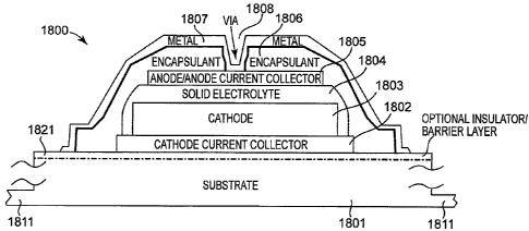
Figure 18 is a schematic cross-section view of a solid-state-cell 1800
10 showing contact areas and/or layers of the cell that are photo-
lithographically
defined. Optionally, photo-lithographic techniques are also used to singulate
the cell
with the exception of optional substrate support tabs. ln some embodiments,
cell
1800 is formed by successive layers deposited on substrate 1801. In other
embodiments, some of the successive layers are deposited on substrate 1801,
while
15 other layers are deposited on a top-side layer that is then laminated to
the substrate
and its layers, as described in U.S. Patent Application 11/458,091 cited
above. In
some embodiments, substrate 1801 is covered by cathode current collector layer
1802, cathode material 1803, electrolyte layer 1804 (e.g., LiPON, or a
plurality of
electrolyte layers as described in U.S. Patent Application 11/458,091 cited
above),
20 anode current collector layer 1805 in the case where the battery is charged
after
assembly (or an anode material followed by anode current collector layer 1805
in the
case where the anode material is deposited first), encapsulant 1807, and metal
layer
1807 (which contacts anode current collector layer 1805 through a hole or via
through encapsularit 1807).
Some embodiments use, for substrate layer 1801, silicon, alumina, copper,
stainless steel or aluminum. In some embodiments, substrate thickness ranges
from
0.00 1" for the metal foils, to approximately 0.030" for silicon and alumina.
The battery size can range from about 1 mm square or smaller to as large as
2 square centimeters or larger. Batteries in this size range give practical
amounts of
discharge capacity and are also economically practical for manufacturing.
Batteries
can be square, rectangular, circular, or of myriad other shapes as required by
the
application.
CA 02658092 2009-01-16
WO 2008/011061 PCT/US2007/016276
21
In some embodiments, the construction of the battery begins with the
deposition of the cathode current collector 1801, except in the case of the
metal foil,
where the substrate can serve as the current collector. In some such
embodiments,
the substrate is covered by an insulating layer (e.g., Si02 which insulates
the
cathode-contact substrate from the top metal layer 1807), which is then
pattemed to
leave a hole in the insulator for the cathode contact. The current collector
1801, in
some embodiments, includes a Ti/Ni stack, with the Ti deposited directly on
the
substrate to promote adhesion, with the Ni in contact with the cathode 1803,
as the
cathode (e.g., LiCoO2) adheres well to it. Another approach uses Al/Ni, the Al
serving as a stress-relieving layer to prevent or reduce nucleation sites and
prevent
cracks from occurring in the cathode, particularly as the cathode thickness is
increased to several microns. In some embodiments, the current collector film
thickness is about 0.05 to 0.2 microns for the Ti, and about 0.1 to 0.5
microns for the
Ni. Where Al is used, the film thickness ranges from about 0.5 to 9 microns.
After
using photoresist to pattern the current collector, and wet or dry etch
chemistries to
define the current collector, the resist is removed using solvents and plasma
Oz
chemistries and the next layer is deposited - in this case, the cathode.
In some embodiments, the cathode 1803 thickness ranges from about 3 to 15
microns, depending on the charge/discharge capacity requirements for a given
application. This material is typically LiCoO2. Cathodes less than about 3
microns
thick have also been produced, but the discharge capacity for a micro-battery
is
usually too low to satisfy the application requirements. There are cases
whereby a
thin cathode is sufficient, and the manufacturing techniques and battery
geometries
apply to these thin cathode devices as well. ln some embodiments, the cathode
is
then patterned using a positive tone photoresist such as SPR 220 and etched
using a
wet chemistry. The overlay of the cathode relative to the underlying cathode
current
collector is about 5 to 20 microns per edge (undersized). The photomask is
sized to
account for worst case misalignment between the two layers, and also for size
changes due to the etch and overetch of the two films. The photoresist is
removed
using solvents such as N-Methylpyrrolidone (NMP), optionally coupled with
plasma
02 chemistries. The sidewall profile of the cathode is important, as it
determines
how well the subsequent layers (e.g., LiPON, anode metal, etc.) will cover
that
CA 02658092 2009-01-16
WO 2008/011061 PCT/US2007/016276
22
sidewall. A steep or re-entrant sidewall results in poor step coverage and in
some
cases, discontinuous film coverage. This has implications for subsequent
processing
complexity, hermeticity, and reliability; thus a sloped sidewall is desirable.
Shadow-
masked depositions naturally result in a long, tapered profile, extending as
much as
s 100 microns or more as measured from the point where the film is full
thickness, to
the point where it tapers to nothing. In photo-patterned and wet etched
LiCoO2, the
sidewall can be made to be vertical, sloped negatively, or sloped positively -
the
latter case being the preferred slope. A slope of 20 to 70 degrees off of
normal is
suitable for preventing the undesirable side effects of a vertical or re-
entrant
sidewall, while not sacrificing too much device area to the tapered region of
the
film. This range of angles can be achieved using the appropriate combination
of
photoresist material, exposure, develop time, LiCoO2 etch chemistry, and etch
parameters (e.g., temperature, agitation, etc.).
Once the cathode has been pattemed, it is annealed and the solid electrolyte,
LiPON 1804, is then deposited, photo-patterned using a negative tone
photoresist
such as various polyimides from HD Microsystems, such as the 2720 series,
which
includes 2727, 2723, 2729; the 2-770 series which includes 2770 and 2772; the
2730
series which includes 2731 and 2737; and photodefinable silicones such as WL-
5351
and WL-3010 from Dow Chemical Company. Since the LiPON is water soluble,
most commercially available positive tone resists are not suitable for
patteming
LiPON because of the water-based developers used with these photoresists. The
electrolyte thickness is typically about 0.5 to 2.5 microns thick.
Alternately, the
LiPON can be deposited prior to patterning the cathode, followed with the
patterning
of the cathode as stated above. In the first case, the LiPON extent can be
either
undersized or oversized relative to the underlying cathode; in the latter
case, the
LiPON must be undersized relative to the cathode in order for the cathode
photomask pattern to extend beyond the LiPON. The LiPON border can extend
beyond the cathode current collector edge, or be terminated short of the
current
collector border. By confining the LiPON to within the current collector
border,
contact to the cathode can be made by leaving that current collector, or a
portion of
it, exposed for later access for wirebonding, soldering, conductive epoxy,
etc. When
a top and bottom surface contacting scheme is to be used, the cathode current
CA 02658092 2009-01-16
WO 2008/011061 PCT/US2007/016276
23
collector is accessed through the conductive substrate instead.
Overlay/underlay
distances are about 5 to 20 microns per edge. The photoresist is removed using
non-
aqueous solvents and optionally plasma OZ chemistries.
The anode and/or anode current collector 1805 is then deposited, at a
thickness of about 0.5 to 3 microns. Either Cu or Ti or Ni can be used here as
the
anode current collector Li-plating anodes. Aluminum can also be used, though
it will
serve as an alloying, rather than a plating, anode, and device performance,
charging
voltage, etc. will differ. In some embodiments, the anode must reside either
fully
atop the LiPON in the case where the LiPON is undersized relative to the
cathode
(else the battery will be electrically shorted), or, in the case where LiPON
is
oversized relative to the cathode, the anode can be undersized or oversized
relative
to the cathode and the LiPON. In the case where the substrate is conductive,
or
where the cathode current collector extends beyond the LiPON perimeter, the
anode
must not extend beyond the LiPON perimeter, else the device will be shorted as
well. In some embodiments, the anode is pattemed using either negative tone or
positive tone photoresist, depending on whether the underlying LiPON will be
exposed to the photoresist developer or other aqueous solutions during the
formation
of the anode. Again, typical overlap/underlap distances range from about 5 to
20
microns per edge. In some embodiments, the anode is etched with reactive ion
etching (RIE) in the case of Ti and Al, and with wet chemistries in the case
of Cu
and Ni. In some embodiments, wet chemistries can also be used for etching Ti
and
Al, but dry etching is preferred for the sake of cleanliness and etch control,
and to
prevent wet chemistries from inadvertently etching the LiPON in the case of
using
aqueous etch solutions. In some embodiments, the anode is also shaped prior to
shaping any of the underlying materials. In some embodiments, the photoresist
is
removed using a combination of solvents and plasma 02 chemistries. In the case
of a
pyramidal stack that has one or more successively deposited layer subsequently
undersized relative to the film directly beneath it, the layers having such a
configuration in the battery stack could be deposited sequentially, then
patterned
beginning with the uppermost undersized layer in the stack.
In some embodiments, the next step is to encapsulate - or passivate - the
device and, in one rendition, bring the anode/anode current collector to the
perimeter
CA 02658092 2009-01-16
WO 2008/011061 PCT/US2007/016276
24
of the battery for access in order to wirebond, solder, -connect with
conductive
epoxy, etc. The encapsulation is desirable in order to protect the battery
materials
from exposure to water vapor, oxygen, and other environmental contaminants.
Lithium reacts readily with other elements and compounds, and therefore should
be
isolated from the outside world after production of the battery. In some
embodiments, this is accomplished through the use of a multilayer, alternating
stack
of spin-on material - usually an organic material is used for each layer 1806
such as
a silicone, polyimide, epoxy or other such polymer as discussed above - for
the
purpose of smoothing out defects and nonplanar surfaces, and then a
metallization
layer 1807, such as Al or Cu, is deposited, in an alternating fashion, for the
purpose
of preventing the migration of external contaminants into the active battery
structure. In an embodiment of the present invention, an alternating
encapsulating
structure comprising one or more layers of nitride and one or more metal
layers is
contemplated. In some embodiments, each successive layer of this multilayer
stack
extends beyond the border of the preceding layer by about 15 to 30 microns.
This
provides a seal ring. The organic layer thickness is about 8 to 10 microns and
includes a via for allowing the overlying metal layer to be electrically
connected to
the anode/anode current collector. The metallization is typically about I to 3
microns
thick for each deposited layer. The final layer is usually silicon nitride, at
a thickness
of about 0.5 to 1 microns, which provides additional hermetic protection and
is
compatible with integrated circuit packaging materials. It also serves as
something
of a physical barrier to abrasion and handling damage. In the case where the
substrate is used to make contact to.the cathode cun:ent collector, the
cathode current
collector can be completely sealed, thus providing a better hermetic seal
compared
with the case in which a cathode current collector tab must remain exposed
during
the passivation process for later access for electrical connection. An
alternate
approach to the multilayer stack of organic/metal/organic/metal is to using a
single
smoothing layer of organic material, then electroplate a thick layer of copper
or
nickel or gold in order to provide the moisture and oxygen barrier and
electrical
contact to the anode.
In some embodiments, for some of the layers in the battery stack, it is also
desirable to chamfer the corners, rather than having right angles. In some
CA 02658092 2009-01-16
WO 2008/011061 PCT/US2007/016276
embodiments, this is accomplished by forming a corner in the photomask using
two
or more line segments. The photo and etch processes will naturally round the
corner
more gradually than as drawn on the photomask. In some embodiments, the
benefit
is in stress relief primarily, to reduce the likelihood of stress fracturing
of the films.
5 A secondary benefit is that the photoresist coverage over the tall
sidewalls,
particularly as the cathodes are made thicker, will be increased relative to a
structure
having a right angle.
One aspect of some embodiments of the invention includes an apparatus that
includes a substrate having an anode contact, a LiPON electrolyte separator
io deposited on the anode contact, and a plated layer of lithium anode
material between
the LiPON and the anode contact.
In some embodiments, the anode contact includes copper and the substrate
includes a polymer.
Another aspect of the invention includes an apparatus including a deposition
15 station that deposits LiPON onto an anode contact, an optional plating
station that
plates lithium onto the anode contact to form an anode substrate, a cathode-
deposition station that deposits a cathode material onto a substrate and
deposits
LiPON onto the cathode material to form a cathode substrate, and an assembly
station that assembles the anode substrate to the cathode substrate using a
polymer
20 electrolyte material sandwiched between the cathode substrate and the anode
substrate.
In some embodiments of the invention, the deposition station comprises
sputter deposition of LiPON.
In some embodiments, the LiPON is deposited onto the anode contact with a
25 _ thickness of between about 0.1 microns and about l micron. In some
embodiments,
the anode's LiPON layer is less than 0.1 microns thick. In some embodiments,
this
LiPON layer is about 0.1 microns. In some embodiments, this LiPON layer is
about
0.2 microns. In some embodiments, this LiPON layer is about 0.3 microns. In
some
embodiments, this LiPON layer is about 0.4 microns. In some embodiments, this
LiPON layer is about 0.5 microns. In some embodiments, this LiPON layer is
about
0.6 microns. In some embodiments, this LiPON layer is about 0.7 microns. In
some
embodiments, this LiPON layer is about 0.8 microns. In some embodiments, this
CA 02658092 2009-01-16
WO 2008/011061 PCT/US2007/016276
26
LiPON layer is about 0.9 microns. In some embodiments, this LiPON layer is
about
1.0 microns. In some embodiments, this LiPON layer is about 1.1 microns. In
some
embodiments, this LiPON layer is about 1.2 microns. In some embodiments, this
LiPON layer is about 1.3 microns. In some embodiments, this LiPON layer is
about
1.4 microns. In some embodiments, this LiPON layer is abotit 1.5 microns. In
some
embodiments, this LiPON layer is about 1.6 microns. In some embodiments, this
LiPON layer is about 1.7 microns. In some embodiments, this LiPON layer is
about
1.8 microns. In some embodiments, this LiPON layer is about 1.9 microns. In
some
embodiments, this LiPON layer is about 2.0 microns. In some embodiments, this
LiPON layer is about 2.1 microns. In some embodiments, this LiPON layer is
about
2.2 microns. In some embodiments, this LiPON layer is about 2.3 microns. In
some
embodiments, this LiPON layer is about 2.4 microns. In some embodiments, this
LiPON layer is about 2.5 microns. In some embodiments, this LiPON layer is
about
2.6 microns. In some embodiments, this LiPON layer is about 2.7 microns. In
some
embodiments, this LiPON layer is about 2.8 microns. In some embodiments, this
LiPON layer is about 2.9 microns. In some embodiments, this LiPON layer is
about
3 microns. In some embodiments, this LiPON layer is about 3.5 microns. In some
embodiments, this LiPON layer is about 4 microns. In some embodiments, this
LiPON layer is about 4.5 microns. In some embodiments, this LiPON layer is
about
5 microns. In some embodiments, this LiPON layer is about 5.5 microns. In some
embodiments, this LiPON layer is about 6 microns. In some embodiments, this
LiPON layer is about 7 microns. In some embodiments, this LiPON layer is about
8
microns. In some embodiments, this LiPON layer is about 7 microns. In some
embodiments, this LiPON layer is about 9 microns. In some embodiments, this
LiPON layer is about 10 microns. ln some embodiments, this LiPON layer is more
than 10 microns.
In some embodiments, the LiPON is deposited onto the cathode contact with
a thickness of between about 0.1 microns and about 1 micron. In some
embodiments, the cathode's LiPON layer is less than 0.1 microns thick. In some
embodiments, this LiPON layer is about 0.1 microns. In some embodiments, this
LiPON layer is about 0.2 microns. In some embodiments, this LiPON layer is
about
0.3 microns. In some embodiments, this LiPON layer is about 0.4 microns. In
some
CA 02658092 2009-01-16
WO 2008/011061 PCT/US2007/016276
27
embodiments, this LiPON layer is about 0.5 microns. In some embodiments, this
LiPON layer is about 0.6 microns. In some embodiments, this LiPON layer is
about
0.7 microns. In some embodiments, this LiPON layer is about 0.8 microns. In
some
embodiments, this LiPON layer is about 0.9 microns. In some embodiments, this
LiPON layer is about 1.0 microns. In some embodiments, this LiPON layer is
about
1.1 microns. In some embodiments, this LiPON layer is about 1.2 microns. In
some
embodiments, this LiPON layer is about 1.3 microns. In some embodiments, this
LiPON layer is about 1.4 microns. In some embodiments, this LiPON layer is
about
1.5 microns. In some embodiments, this LiPON layer is about 1.6 microns. In
some
embodiments, this LiPON layer is about 1.7 microns. In some embodiments, this
LiPON layer is about 1.8 microns. In some embodiments, this LiPON layer is
about
1.9 microns. In some embodiments,. this LiPON layer is about 2.0 microns. In
some
embodiments, this LiPON layer is about 2.1 microns. In some embodiments, this
LiPON layer is.about 2.2 microns. In some embodiments, this LiPON layer is
about
2.3 microns. In some embodiments, this LiPON layer is about 2.4 microns. In
some
embodiments, this LiPON layer is about 2.5 microns. In some embodiments, this
LiPON layer is about 2.6 microns. In some embodiments, this LiPON layer is
about
2.7 microns. In some embodiments, this LiPON layer is about 2.8 microns. In
some
embodiments, this LiPON layer is about 2.9 microns. In some embodiments, this
LiPON layer is about 3 microns. In some embodiments, this LiPON layer is about
3.5 microns. In some embodiments, this LiPON layer is about 4 microns. In some
embodiments, this LiPON layer is about 4.5 microns. In some embodiments, this
LiPON layer is about 5 microns. In some embodiments, this LiPON layer is about
5.5 microns. In some embodiments, this LiPON layer is about 6 microns. In some
embodiments, this LiPON layer is about 7 microns. In some embodiments, this
LiPON layer is about 8 microns. In some embodiments, this LiPON layer is about
7
microns. In some embodiments, this LiPON layer is about 9 microns. In some
embodiments, this LiPON layer is about 10 microns. In some embodiments, this
LiPON layer is more than 10 microns.
In some embodiments, the plating station performs electroplating at densities
of about 0.9 mA/cm2 and voltage of about 40 mV at 0.6 mA between a lithium
counterelectrode and the plated lithium of the anode.
CA 02658092 2009-01-16
WO 2008/011061 PCT/US2007/016276
28
In some embodiments of the invention, the lithium is conducted through a
liquid propylene carbonate/LiPF6 electrolyte solution and the LiPON
barrier/electrolyte layer for the lithium to be plated onto the anode
connector. In
. some embodiments of the invention, the lithium is conducted through a liquid
propylene carbonate/LiPF6 electrolyte solution and the LiPON
barrier/electrolyte
layer for the lithium to be plated onto the cathode connector.
Some embodiments of the invention include an apparatus that includes a
battery having an anode, a cathode, and an electrolyte structure, wherein the
anode
includes an anode material that includes lithium and a LiPON
barrier/electrolyte
io layer covering at least a portion of the anode; the cathode includes a
cathode
material that includes lithium and a LiPON barrier/electrolyte layer covering
at least
a portion of the cathode; and the electrolyte structure includes a polymer
electrolyte
material sandwiched between the LiPON barrier/electrolyte layer covering the
anode
and the LiPON barrier/electrolyte layer covering the cathode.
In some embodiments of the apparatus, the cathode material includes LiCoO2
deposited on a cathode contact material, and then the LiPON
barrier/electrolyte layer
covering the cathode is deposited.
In some embodiments of the apparatus, the lithium anode material is plated
onto a copper anode contact through LiPON barrier/electrolyte layer covering
the
anode.
In some embodiments of the apparatus, the anode material is deposited on
both major faces of a metal sheet at least partially covered by the LiPON
barrier/electrolyte layer.
In some embodiments of the apparatus, the cathode material is deposited on
both major faces of a metal sheet and is at least partially covered by the
LiPON
barrier/electrolyte layer.
In some embodiments of the apparatus, the cathode contact material includes
a metal mesh around which the cathode material is deposited.
In some embodiments of the apparatus, the lithium anode material is plated
onto both major faces of an anode contact foil through LiPON
barrier/electrolyte
layer covering the anode contact layer.
CA 02658092 2009-01-16
WO 2008/011061 PCT/US2007/016276
29
In some embodiments of the apparatus, the lithium anode material is plated
onto a first major face of a contact foil through LiPON barrier/electrolyte
layer
covering the contact foil the lithium cathode material is deposited onto a
second
major face of the contact foil, and the LiPON barrier/electrolyte layer
covering the
cathode is then deposited by sputtering.
. In some embodiments of the appaiatus, the lithium cathode material is
deposited onto both major faces of a cathode contact foil, and the LiPON
barrier/electrolyte layer covering the cathode is then deposited by
sputtering.
In some embodiments of the apparatus, the lithium cathode material is
deposited onto both major faces of a cathode contact mesh, and the LiPON
barrier/electrolyte layer covering the cathode is then deposited by
sputtering.
In some embodiments, another aspect of the invention includes a method that
includes providing a first sheet that includes an anode material that includes
lithium
and a LiPON barrier/electrolyte layer covering the anode material; providing a
second sheet that includes a cathode material that includes lithium and a
LiPON
barrier/electrolyte layer covering the cathode material; and sandwiching a
polymer
electrolyte material between the LiPON barrier/electrolyte layer covering the
anode
material of the first sheet and the LiPON barrier/electrolyte layer covering
the
cathode material of the first cathode sheet.
Some embodiments of the method further include providing a third sheet that
includes an anode material that includes lithium and a LiPON
barrier/electrolyte
layer covering the anode material; providing a fourth sheet that includes a
cathode
material that includes lithium and a LiPON barrier/electrolyte layer covering
the
cathode material; sandwiching a polymer electrolyte material between the LiPON
barrier/electrolyte layer covering the anode material of the third sheet and
the
LiPON barrier/electrolyte layer covering the cathode material of the fourth
sheet;
and sandwiching a polymer electrolyte material between the LiPON
barrier/electrolyte layer covering the anode material of the first sheet and
the LiPON
barrier/electrolyte layer covering the cathode material of the fourth sheet.
In some embodiments of the method, the anode is deposited as a layer on a
copper anode contact layer through a LiPON layer.
CA 02658092 2009-01-16
WO 2008/011061 PCT/US2007/016276
ln some embodiments of the method, the deposition of a lithium anode is
done by electroplating in a propylene carbonate/LiPF6 electrolyte solution.
In some embodiments of the method, the first sheet includes a cathode
material on a face opposite the anode material and a LiPON barrier/electrolyte
layer
s covering the cathode material, and the second sheet includes an anode
material that
includes lithium and a LiPON barrier/electrolyte layer covering the anode
material,
and the method further includes providing a third sheet that includes an anode
material that includes lithium and a LiPON barrier/electrolyte layer covering
the
anode material on a first face, and an anode material that includes lithium
and a
10 LiPON barrier/electrolyte layer covering the anode material on a second
face
opposite the first face; and sandwiching a polymer electrolyte material
between the
LiPON barrier/electrolyte layer covering the anode material of the first sheet
and the
LiPON barrier/electrolyte layer covering the cathode material of the third
sheet.
In some embodiments, another aspect of the invention includes an apparatus
15 that includes a first sheet that includes an anode material that includes
lithium and a
LiPON barrier/electrolyte layer covering the anode material; a second sheet
that
includes a cathode material that includes lithium and a LiPON
barrier/electrolyte
layer covering the cathode material; and means for sandwiching a polymer
electrolyte material between the LiPON barrier/electrolyte layer covering the
anode
20 material of the first sheet and the LiPON barrier/electrolyte layer
covering the
cathode material of the first cathode sheet.
Some embodiments of this apparatus include a third sheet that includes an
anode material that includes lithium and a LiPON barrier/electrolyte layer
covering
the anode material; a fourth sheet that includes a cathode material that
includes
25 lithium and a LiPON barrier/electrolyte layer covering the cathode
material; means
for sandwiching a polymer electrolyte material between the LiPON
barrier/electrolyte layer covering the anode material of the third sheet and
the
LiPON barrier/electrolyte layer covering the cathode material of the fourth
sheet;
and means for sandwiching a polymer electrolyte material between the LiPON
30 barrier/electrolyte layer covering the anode material of the first sheet
and the LiPON
barrier/electrolyte layer covering the cathode material of the fourth sheet.
CA 02658092 2009-01-16
WO 2008/011061 PCT/US2007/016276
31
In some embodiments, the invention includes a method that includes
providing a first sheet that includes a substrate, a cathode material, an
anode current
collector, an optional anode material, and an electrolyte layer separating the
cathode
material from the anode current collector; and performing a one or more
material
removal operations through the cathode material, the anode current collector,
and the
electrolyte layer separating the cathode material from the anode current
collector,
and removing a first portion of the substrate but not through a second portion
of the
substrate so as to leave a first plurality of battery cells that are separated
from one
another but wherein a plurality of the first plurality of battery cells
remains attached
to at least a single un-separated part of the first sheet.
Some embodiments of the method further include depositing a second
material on the sheet to cover the plurality of cells at least on their sides.
Some embodiments of the method further include performing a first
material-removal operation to remove a sub-portion of the second material to
1s separate a plurality of cells from each other.
In some embodiments, the second material is an electrical insulator deposited
to passivate the cells.
In some embodiments, the second material includes LiPON_
In some embodiments, the material-removal operations include laser
ablation.
In some embodiments, the material-removal operations include
photolithography.
In some embodiments, the material-removal operations form trenches
between cells having a width of about 10 microns or less.
Some embodiments of the method further include depositing a passivation
material on the sheet to cover the plurality of cells at least on their sides.
In some embodiments, the invention includes an apparatus that includes a
source of a first sheet that includes a substrate, a cathode material, and
anode current
collector, an optional anode material, and an electrolyte layer separating the
cathode
material from the anode current collector; and means for removing material
through
the cathode material, the anode current collector, and the electrolyte layer
separating
the cathode material from the anode current collector, and through a first
portion of
CA 02658092 2009-01-16
WO 2008/011061 PCT/US2007/016276
32
the substrate but not through a second portion of the substrate so as to leave
a
plurality of battery cells that are separated from one another but each one of
the
plurality of battery cells remaining attached to at least a single part of the
first sheet.
Some embodiments of the apparatus further include means for depositing a
second material on the sheet to cover the plurality of cells at least on their
sides; and
means for removing material a sub-portion of the second material to separate a
plurality of cells from each other.
Some embodiments of the apparatus further include means for depositing a
second material on the sheet to cover the plurality of cells at least on their
sides.
In some embodiments, the second material is an electrical insulator deposited
to passivate the cells. In some embodiments, the second material includes
LiPON. In
some embodiments, the means for removing include laser ablation. In some
embodiments, the means for removing include photolithography. In some
embodiments, the material-removal operations form trenches between cells
having a
width of about 10 microns or less.
In some embodiments, the invention includes an apparatus that includes a
source of a first sheet that includes a substrate, a cathode material, an
anode current
collector, an optional anode material, and an electrolyte layer separating the
cathode
material from the anode current collector; and a first material removal
station
configured to remove the cathode material, the anode current collector, and
the
electrolyte layer separating the cathode material from the anode current
collector,
and through a first portion'of the substrate but not through a second portion
of the
substrate so as to leave a plurality of battery cells that are separated from
one
another but each one of the plurality of battery cells remaining attached to
at least a
single part of the first sheet.
Some embodiments of the apparatus further include a deposition station that
deposits a passivation material on the sheet to cover the plurality of cells
at least on
their sides; and a second material removal station configured to remove a sub-
portion of the second material to separate a plurality of cells from each
other.
Alternatively, the method and apparatus may comprise the further deposition
station
that deposits a passivation material on the sheet to cover the plurality of
cells at least
on their sides as noted above, and the first material removal station may be
CA 02658092 2009-01-16
WO 2008/011061 PCT/US2007/016276
33
positioned after the further deposition station and configured to remove the
passivation material, the cathode material, the anode current collector, and
the
electrolyte layer separating the cathode.material from the anode current
collector,
and through a first portion of the substrate but not through a second portion
of the
substrate so as to leave a plurality of battery cells that are separated from
one
another but each one of the plurality of battery cells remaining attached to
at least a
single part of the first sheet.
In some embodiments, the passivation material includes one or more metal
layers alternating with one or more polymer layers.
ln some embodiments, first sheet includes a cathode material on a face
opposite the anode material and a LiPON barrier/electrolyte layer covering the
cathode material, and the second sheet includes an anode material that
includes
lithium and a LiPON barrier/electrolyte layer covering the anode material; and
the
apparatus further includes a third sheet that includes an anode material that
includes
lithium and a LiPON barrier/electrolyte layer covering the anode material on a
first
face, and an anode material that includes lithium and a LiPON
barrier/electrolyte
layer covering the anode material on a second face opposite the first face;
and means
for sandwiching a polymer electrolyte material between the LiPON
barrier/electrolyte layer covering the anode material of the first sheet and
the LiPON
barrier/electrolyte layer covering the cathode material of the third sheet.
It is to be understood that the above description is intended to be
illustrative,
and not restrictive. Although numerous characteristics and advantages of
various
embodiments as described herein have been set forth in the foregoing
description,
together with details of the structure and function of various embodiments,
many
other embodiments and changes to details will be apparent to those of skill in
the art
upon reviewing the above description. The scope of the invention should be,
therefore, determined with reference to the appended claims, along with the
full
scope of equivalents to which such claims are entitled. In the appended
claims, the
terms "including" and "in which" are used as the plain-English equivalents of
the
respective terms "comprising" and "wherein," respectively. Moreover, the,terms
"first," "second," and "third," etc., are used merely as labels, and are not
intended to
impose numerical requirements on their objects.