Note: Descriptions are shown in the official language in which they were submitted.
CA 02658106 2009-01-16
WO 2008/011238 PCT/US2007/071330
THERMAL PROTECTION FOR LAMP BALLASTS
CROSS REFERENCE TO RELATED APPLICATIONS
[0001] This application claims priority to United States Patent Application
Serial No.
11/489,145, filed July 18, 2006, entitled "Thermal Protection for Lamp
Ballasts", which is
hereby incorporated by reference in its entirety.
FIELD OF THE INVENTION
[0002] This invention relates to thermal protection for lamp ballasts.
Specifically, this
invention relates to a ballast having active thermal management and protection
circuitry that
allows the ballast to safely operate when a ballast over-temperature condition
has been detected,
allowing the ballast to safely continue to provide power to the lamp.
BACKGROUND OF THE INVENTION
[0003] Lamp ballasts are devices that convert standard line voltage and
frequency to a
voltage and frequency suitable for a specific lamp type. Usually, ballasts are
one component of a
lighting fixture that receives one or more fluorescent lamps. The lighting
fixture may have more
than one ballast.
[0004] Ballasts are generally designed to operate within a specified operating
temperature. The maximum operating temperature of the ballast can be exceeded
as the result of
a number of factors, including improper matching of the ballast to the
lamp(s), improper heat
sinking, and inadequate ventilation of the lighting fixture. If an over-
temperature condition is
not remedied, then the ballast and/or lamp(s) may be damaged or destroyed.
[0005] Some prior art ballasts have circuitry that shuts down the ballast upon
detecting
an over-temperature condition. This is typically done by means of a thermal
cut-out switch that
senses the ballast temperature. When the switch detects an over-temperature
condition, it shuts
down the ballast by removing its supply voltage. If a normal ballast
temperature is subsequently
achieved, the switch may restore the supply voltage to the ballast. The result
is lamp flickering
and/or a prolonged loss of lighting. The flickering and loss of lighting can
be annoying. In
addition, the cause may not be apparent and might be mistaken for malfunctions
in other
electrical systems, such as the lighting control switches, circuit breakers,
or even the wiring.
-1-
CA 02658106 2009-01-16
WO 2008/011238 PCT/US2007/071330
SUMMARY OF THE INVENTION
[0006] A lamp ballast has temperature sensing circuitry and control circuitry
responsive
to the temperature sensor that limits the output current provided by the
ballast when an over-
temperature condition has been detected. The control circuitry actively
adjusts the output current
as long as the over-temperature condition is detected so as to attempt to
restore an acceptable
operating temperature while continuing to operate the ballast (i.e., without
shutting down the
ballast). The output current is maintained at a reduced level until the sensed
temperature returns
to the acceptable temperature.
[0007] Various methods for adjusting the output current are disclosed. In one
embodiment, the output current is linearly adjusted during an over-temperature
condition. In
another embodiment, the output current is adjusted in a step function during
an over-temperature
condition. In yet other embodiments, both linear and step function adjustments
to output current
are employed in differing combinations. In principle, the linear function may
be replaced with
any continuous decreasing function including linear and non-linear functions.
Gradual, linear
adjustment of the output current tends to provide a relatively imperceptible
change in lighting
intensity to a casual observer, whereas a stepwise adjustment may be used to
create an obvious
change so as to alert persons that a problem has been encountered and/or
corrected.
[0008] The invention has particular application to (but is not limited to)
dimming ballasts
of the type that are responsive to a dimming control to dim fluorescent lamps
connected to the
ballast. Typically, adjustment of the dimming control alters the output
current delivered by the
ballast. This is carried out by altering the duty cycle, frequency or pulse
width of switching
signals delivered to a one or more switching transistors in the output circuit
of the ballast. These
switching transistors may also be referred to as output switches. An output
switch is a switch,
such as a transistor, whose duty cycle and/or switching frequency is varied to
control the output
current of the ballast. A tank in the ballast's output circuit receives the
output of the switches to
provide a generally sinusoidal (AC) output voltage and current to the lamp(s).
The duty cycle,
frequency or pulse width is controlled by a control circuit that is responsive
to the output of a
phase to DC converter that receives a phase controlled AC dimming signal
provided by the
dimming control. The output of the phase to DC converter is a DC signal having
a magnitude
that varies in accordance with a duty cycle value of the dimming signal.
Usually, a pair of
voltage clamps (high and low end clamps) is disposed in the phase to DC
converter for the
purpose of establishing high end and low end intensity levels. The low end
clamp sets the
minimum output current level of the ballast, while the high end clamp sets its
maximum output
current level.
-2-
CA 02658106 2009-01-16
WO 2008/011238 PCT/US2007/071330
[0009] According to one embodiment of the invention, a ballast temperature
sensor is
coupled to a foldback protection circuit that dynamically adjusts the high end
clamping voltage
in accordance with the sensed ballast temperature when the sensed ballast
temperature exceeds a
threshold. The amount by which the high end clamping voltage is adjusted
depends upon the
difference between the sensed ballast temperature and the threshold. According
to another
embodiment, the high and low end clamps need not be employed to implement the
invention.
Instead, the foldback protection circuit may communicate with a multiplier,
that in turn
communicates with the control circuit. In this embodiment, the control circuit
is responsive to
the output of the multiplier to adjust the duty cycle, pulse width or
frequency of the switching
signal.
[0010] The invention may also be employed in connection with a non-dimming
ballast in
accordance with the foregoing. Particularly, a ballast temperature sensor and
foldback protection
are provided as above described, and the foldback protection circuit
communicates with the
control circuit to alter the duty cycle, pulse width or frequency of the one
or more switching
signals when the ballast temperature exceeds the threshold.
[0011] In each of the embodiments, a temperature cutoff switch may also be
employed to
remove the supply voltage to shut down the ballast completely (as in the prior
art) if the ballast
temperature exceeds a maximum temperature threshold.
[0012] According to another embodiment of the present invention, a circuit for
controlling output current from a ballast to a lamp comprises a temperature
sensor and a
programmable controller. The temperature sensor is thermally coupled to the
ballast to provide a
temperature signal having a magnitude indicative of ballast temperature, Tb.
The programmable
controller is operable to cause the ballast to enter a current limiting mode
when the magnitude of
the temperature signal indicates that Tb has exceeded a predetermined ballast
temperature, T1.
The programmable controller causes the output current to be responsive to the
temperature signal
according to one of (i) a step function or (ii) a combination of step and
continuous functions,
while continuing to operate the ballast.
[0013] In addition, the present invention provides a thermally protected
ballast, which
comprises a front end AC-to-DC converter, a back end DC-to-AC converter, a
temperature
sensor, and a programmable controller. The front end AC-to-DC converter
receives a supply
voltage, while the back end DC-to-AC converter is coupled to the front end AC-
to-DC converter
for providing output current to a load. The temperature sensor is adapted to
provide a
temperature signal having a magnitude indicative of a temperature of the
ballast, Tb. The
programmable controller is responsive to the temperature signal and operable
to cause the
-3-
CA 02658106 2009-01-16
WO 2008/011238 PCT/US2007/071330
DC-to-AC circuit to adjust the output current. The temperature signal causes
the programmable
controller to adjust the output current in response to a detected over-
temperature condition,
according to one of (i) a step function or (ii) a combination of step and
linear functions, while
continuing to operate the ballast.
[0014] The present invention further provides a method of controlling a
ballast
comprising the steps of: a) determining a temperature Tb of the ballast; b)
comparing the
temperature Tb to a first reference temperature T1; and c) controlling an
output current provided
by the ballast according to one of (i) a step function or (ii) a combination
of a step and
continuous functions, while continuing to operate the ballast, in accordance
with the result of
step (b).
[0015] Other features of the invention will be evident from the following
detailed
description of the preferred embodiments.
BRIEF DESCRIPTION OF THE DRAWINGS
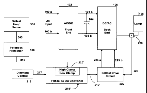
[0016] Figure 1 is a functional block diagram of a prior art non-dimming
ballast.
[0017] Figure 2 is a functional block diagram of a prior art dimming ballast.
[0018] Figure 3 is a functional block diagram of one embodiment of the present
invention as employed in connection with a dimming ballast.
[0019] Figure 4a graphically illustrates the phase controlled output of a
typical dimming
control.
[0020] Figure 4b graphically illustrates the output of a typical phase to DC
converter.
[0021] Figure 4c graphically illustrates the effect of a high and low end
clamp circuit on
the output of a typical phase to DC converter.
[0022] Figure 5a graphically illustrates operation of an embodiment of the
present
invention to linearly adjust the ballast output current when the ballast
temperature is greater than
threshold T1.
[0023] Figure 5b graphically illustrates operation of an embodiment of the
present
invention to reduce the ballast output current in a step function to a level
L1 when the ballast
temperature is greater than threshold T2, and to increase the output current
in a step function to
100 Io when the ballast temperature decreases to a normal temperature T3.
[0024] Figure 5c graphically illustrates operation of an embodiment of the
present
invention to adjust the ballast output current linearly between temperature
thresholds T4 and T5,
to reduce the ballast output current in a step function from level L2 to level
L3 if temperature
threshold T5 is reached or exceeded, and to increase the output current in a
step function to level
L4 when the ballast temperature decreases to threshold T6.
-4-
CA 02658106 2009-01-16
WO 2008/011238 PCT/US2007/071330
[0025] Figure 5d graphically illustrates operation of an embodiment of the
present
invention to adjust the ballast output current in various steps for various
thresholds, and to
further adjust ballast output current linearly between levels L6 and L7 if the
stepwise reductions
in output current are not sufficient to restore the ballast temperature to
normal.
[0026] Figure 6 illustrates one circuit level implementation for the
embodiment of Figure
3 that exhibits the output current characteristics of Figure 5c.
[0027] Figure 7 is a functional block diagram of another embodiment of the
present
invention for use in connection with a dimming ballast.
[0028] Figure 8 is an output current versus temperature response for the
embodiment of
Figure 7.
[0029] Figure 9 is a functional block diagram of an embodiment of the present
invention
that may be employed with a non-dimming ballast.
[0030] Fig. 10 is a simplified block diagram of an electronic dimming ballast
according
to another embodiment of the present invention.
[0031] Fig. 11 is a flowchart of a thermal foldback protection procedure
executed by a
programmable controller of the ballast of Fig. 10 according to the present
invention.
DETAILED DESCRIPTION OF THE PREFERRED EMBODIMENTS
[0032] Turning now to the drawings, wherein like numerals represent like
elements there
is shown in Figures 1 and 2 functional block diagrams of typical prior art non-
dimming and
dimming ballasts, respectively. Referring to Figure 1, a typical non-dimming
ballast includes a
front end AC to DC converter 102 that converts applied line voltage 100a, b,
typically 120 volts
AC, 60 Hz, to a higher voltage, typically 400 to 500 volts DC. Capacitor 104
stabilizes the high
voltage output on 103a, b of AC to DC converter 102. The high voltage across
capacitor 104 is
presented to a back end DC to AC converter 106, which typically produces a 100
to 400 Volt AC
output at 45 KHz to 80 KHz at terminals 107a, b to drive the load 108,
typically one or more
florescent lamps. Typically, the ballast includes a thermal cut-out switch
110. Upon detecting an
over-temperature condition, the thermal cutout switch 110 removes the supply
voltage at 100a to
shut down the ballast. The supply voltage is restored if the switch detects
that the ballast returns
to a normal or acceptable temperature.
[0033] The above description is applicable to Figure 2, except that Figure 2
shows
additional details of the back end DC to AC converter 106, and includes
circuitry 218, 220 and
222 that permits the ballast to respond to a dimming signa1217 from a dimming
contro1216. The
dimming contro1216 may be any phase controlled dimming device and may be wall
mountable.
An example of a commercially available dimming ballast of the type of Figure 2
is model
-5-
CA 02658106 2009-01-16
WO 2008/011238 PCT/US2007/071330
number FDB-T554-120-2, available from Lutron Electronics, Co., Inc.,
Coopersburg, PA, the
assignee of the present invention. As is known, the dimming signal is a phase
controlled AC
dimming signal, of the type shown in Figure 4a, such that the duty cycle of
the dimming signal
and hence the RMS voltage of the dimming signal varies with adjustment of the
dimming
actuator. Dimming signa1217 drives a phase to DC converter 218 that converts
the phase
controlled dimming signa1217 to a DC voltage signa1219 having a magnitude that
varies in
accordance with a duty cycle value of the dimming signal , as graphically
shown in Figure 4b. It
will be seen that the signa1219 generally linearly tracks the dimming
signa1217. However,
clamping circuit 220 modifies this generally linear relationship as described
hereinbelow.
[0034] The signa1219 stimulates ballast drive circuit 222 to generate at least
one
switching control signa1223a, b. Note that the switching control signals 223a,
b shown in Figure
2 are typical of those in the art that drive output switches in an inverter
function (DC to AC) in
the back-end converter 106. An output switch is a switch whose duty cycle
and/or switching
frequency is varied to control the output current of the ballast. The
switching control signals
control the opening and closing of output switches 210, 211 coupled to a tank
circuit 212, 213.
Although Figure 2 depicts a pair of switching control signals, 223a, b, an
equivalent function that
uses only one switching signal may be used. A current sense device 228
provides an output
(load) current feedback signa1226 to the ballast drive circuit 222. The duty
cycle, pulse width or
frequency of the switching control signals is varied in accordance with the
level of the signa1219
(subject to clamping by the circuit 220), and the feedback signa1226, to
determine the output
voltage and current delivered by the ballast.
[0035] High and low end clamp circuit 220 in the phase to DC converter limits
the output
219 of the phase to DC converter. The effect of the high and low end clamp
circuit 220 on the
phase to DC converter is graphically shown in the Figure 4c. It will be seen
that the high and
low clamp circuit 220 clamps the upper and lower ends of the otherwise linear
signa1219 at
levels 400 and 401, respectively. Thus, the high and low end clamp circuitry
220 establishes
minimum and maximum dimming levels.
[0036] A temperature cutoff switch 110 (Figure 1) is also usually employed.
All that has
been described thus far is prior art.
[0037] Figure 3 is a block diagram of a dimming ballast employing the present
invention.
In particular, the dimming ballast of Figure 2 is modified to include a
ballast temperature sensing
circuit 300 that provides a ballast temperature signa1305 to a foldback
protection circuit 310. As
described below, the foldback protection circuit 310 provides an appropriate
adjustment signal
315 to the high and low end clamp circuit 220' to adjust the high cutoff
leve1400. Functionally,
-6-
CA 02658106 2009-01-16
WO 2008/011238 PCT/US2007/071330
clamp circuit 220' is similar to clamp circuit 220 of Figure 2, however, the
clamp circuit 220' is
further responsive to adjustment signa1315, which dynamically adjusts the high
end clamp
voltage (i.e. leve1400).
[0038] The ballast temperature sensing circuit 300 may comprise one or more
thermistors
with a defined resistance to temperature coefficient characteristic, or
another type of temperature
sensing thermostat device or circuit. Foldback protection circuit 310
generates an adjustment
signa1315 in response to comparison of temperature signa1305 to a threshold.
The foldback
protection circuit may provide either a linear output (using a linear response
generator) or a step
function output (using a step response generator), or a combination of both,
if the comparison
determines that an over-temperature condition exists. In principle, the
exemplary linear function
shown in Figure 3 may be replaced with any continuous function including
linear and non-linear
functions. For the purpose of simplicity and clarity, the linear continuous
function example will
be used. But, it can be appreciated that other continuous functions may
equivalently be used.
Regardless of the exact function used, the high end clamp leve1400 is reduced
from its normal
operating level when the foldback protection circuit 310 indicates that an
over-temperature
condition exists. Reducing the high end clamp leve1400 adjusts the drive
signa1219' to the
ballast drive circuit 222 so as to alter the duty cycle, pulse width or
frequency of the switching
control signals 223a, b and hence reduce the output current provided by the
ballast to load 108.
Reducing output current should, under normal circumstances, reduce the ballast
temperature.
Any decrease in ballast temperature is reflected in signa1315, and the high
end clamp leve1400
is increased and/or restored to normal, accordingly.
[0039] Figures 5a - 5d graphically illustrate various examples of adjusting
the output
current during an over-temperature condition. These examples are not
exhaustive and other
functions or combinations of functions may be employed.
[0040] In the example of Figure 5a, output current is adjusted linearly when
the ballast
temperature exceeds threshold T1. If the ballast temperature exceeds T1, the
foldback protection
circuit 310 provides a limiting input to the high end clamp portion of the
clamp circuit 220' so as
to linearly reduce the high end clamp leve1400, such that the output current
may be reduced
linearly from 100% to a preselected minimum. The temperature T1 may be preset
by selecting
the appropriate thresholds in the foldback protection circuit 310 as described
in greater detail
below. During the over-temperature condition, the output current can be
dynamically adjusted in
the linear region 510 until the ballast temperature stabilizes and is
permitted to be restored to
normal. Since fluorescent lamps are often operated in the saturation region of
the lamp (where
an incremental change in lamp current may not produce a corresponding change
in light
-7-
CA 02658106 2009-01-16
WO 2008/011238 PCT/US2007/071330
intensity), the linear adjustment of the output current may be such that the
resulting change in
intensity is relatively imperceptible to a casual observer. For example, a 40%
reduction in output
current (when the lamp is saturated) may produce only a 10% reduction in
perceived intensity.
[0041] The embodiment of the invention of Figure 3 limits the output current
of the load
to the linear region 510 even if the output current is less than the maximum
(100%) value. For
example, referring to Figure 5a, the dimming control signa1217 may be set to
operate the lamp
load 108 at, for example, 80% of the maximum load current. If the temperature
rises to above a
temperature value T1, a linear limiting response is not activated until the
temperature reaches a
value of T1*. At that value, linear current limiting may occur which will
limit the output current
to the linear region 510. This allows the maximum (100%) linear limiting
profile to be utilized
even if the original setting of the lamp was less than 100% load current. As
the current limiting
action of the invention allows the temperature to fall, the lamp load current
will once again
return to the originally set 80% level as long as the dimmer control signa1217
is unchanged.
[0042] In the example of Figure 5b, output current may be reduced in a step
function
when the ballast temperature exceeds threshold T2. If the ballast temperature
exceeds T2, then
the foldback protection circuit 310 provides a limiting input to the high end
portion of the clamp
220' so as to step down the high end clamp leve1400; this results in an
immediate step down in
supplied output current from 100% to level L1. Once the ballast temperature
returns to an
acceptable operating temperature T3, the foldback protection circuit 310
allows the output
current to immediately return to 100%, again as a step function. Notice that
recovery temperature
T3 is lower than T2. Thus, the foldback protection circuit 310 exhibits
hysteresis. The use of
hysteresis helps to prevent oscillation about T2 when the ballast is
recovering from a higher
temperature. The abrupt changes in output current may result in obvious
changes in light
intensity so as to alert persons that a problem has been encountered and/or
corrected.
[0043] In the example of Figure 5c, both linear and step function adjustments
in output
current are employed. For ballast temperatures between T4 and T5, there is
linear adjustment of
the output current between 100% and level L2. However, if the ballast
temperature exceeds T5,
then there is an immediate step down in supplied output current from level L2
to level U. If the
ballast temperature returns to an acceptable operating temperature T6, the
foldback protection
circuit 310 allows the output current to return to level L4, again as a step
function, and the output
current is again dynamically adjusted in a linear manner. Notice that recovery
temperature T6 is
lower than T5. Thus, the foldback protection circuit 310 exhibits hysteresis,
again preventing
oscillation about T5. The linear adjustment of the output current between 100%
and L2 may be
such that the resulting change in lamp intensity is relatively imperceptible
to a casual observer,
-8-
CA 02658106 2009-01-16
WO 2008/011238 PCT/US2007/071330
whereas the abrupt changes in output current between L2 and L3 may be such
that they result in
obvious changes in light intensity so as to alert persons that a problem has
been encountered
and/or corrected.
[0044] In the example of Figure 5d, a series of step functions is employed to
adjust the
output current between temperatures T7 and T8. Particularly, there is a step-
wise decrease in
output current from 100% to level L5 at T7 and another step-wise decrease in
output current
from level L5 to level L6 at T8. Upon a temperature decrease and recovery,
there is a step-wise
increase in output current from level L6 to level L5 at T11, and another step-
wise increase in
output current from level L5 to 100% at T12 (each step function thus employing
hysteresis to
prevent oscillation about T7 and T8). Between ballast temperatures of T9 and
T10, however,
linear adjustment of the output current, between levels L6 and L7, is
employed. Once again, step
and linear response generators (described below) in the foldback protection
circuitry 310 of
Figure 3 allow the setting of thresholds for the various temperature settings.
One or more of the
step-wise adjustments in output current may result in obvious changes in light
intensity, whereas
the linear adjustment may be relatively imperceptible.
[0045] In each of the examples, a thermal cutout switch may be employed, as
illustrated
at 110 in Figure 1, to remove the supply voltage and shut down the ballast if
a substantial over-
temperature condition is detected.
[0046] Figure 6 illustrates one circuit level implementation of selected
portions of the
Figure 3 embodiment. The foldback protection circuit 310 includes a linear
response generator
610 and a step response generator 620. The adjustment signa1315 drives the
output stage 660 of
the phase to DC converter 218' via the high end clamp 630 of the clamp circuit
220'. A low end
clamp 640 is also shown.
[0047] Temperature sensing circuit 300 may be an integrated circuit device
that exhibits
an increasing voltage output with increasing temperature. The temperature
sensing circuit 300
feeds the linear response generator 610 and the step response generator 620.
The step response
generator 620 is in parallel with the linear response generator 610 and both
act in a temperature
dependent manner to produce the adjustment signa1315.
[0048] The temperature threshold of the linear response generator 610 is set
by voltage
divider R3, R4, and the temperature threshold of the step response generator
620 is set by voltage
divider R1, R2. The hysteresis characteristic of the step response generator
620 is achieved by
means of feedback, as is well known in the art.
[0049] The threshold of low end clamp 640 is set via a voltage divider labeled
simply
VDIV1. The phase controlled dimming signa1217 is provided to one input of a
comparator 650.
-9-
CA 02658106 2009-01-16
WO 2008/011238 PCT/US2007/071330
The other input of comparator 650 receives a voltage from a voltage divider
labeled VDIV2. The
output stage 660 of the phase to DC converter 218' provides the control
signa1219'.
[0050] Those skilled in the art will appreciate that the temperature
thresholds of the
linear and step response generators 610, 620 may be set such that the foldback
protection circuit
310 exhibits either a linear function followed by a step function (See Figure
5c), or the reverse.
Sequential step functions may be achieved by utilizing two step response
generators 620 (See
steps L5 and L6 of Figure 5d). Likewise, sequential linear responses may be
achieved by
replacing the step response generator 620 with another linear response
generator 610. If only a
linear function (Figure 5a) or only a step function (Figure 5b) is desired,
only the appropriate
response generator is employed. The foldback protection circuit 310 may be
designed to produce
more than two types of functions, e.g., with the addition of another parallel
stage. For example
the function of Figure 5d may be obtained with the introduction of another
step response
generator 620 to the foldback protection circuit, and by setting the proper
temperature thresholds.
[0051] Figure 7 is a block diagram of a dimming ballast according to another
embodiment of the invention. Again, the dimming ballast of Figure 2 is
modified to include a
ballast temperature sensing circuit 300 that provides a ballast temperature
signa1305 to a
foldback protection circuit 310. The foldback protection circuit 310'
produces, as before, an
adjustment signa1315' to modify the response of the DC to AC back end 106 in
an over-
temperature condition. Nominally, the phase controlled dimming signa1217 from
the dimming
contro1216, and the output of the high and low end clamps 220, act to produce
the control signal
219 that is used, for example, in the dimming ballast of Figure 2. However, in
the configuration
of Figure 7, the control signa1219 and the adjustment signa1315' are combined
via multiplier
700. The resulting product signa1701 is used to drive the ballast drive
circuit 222 in conjunction
with feedback signa1226. It should be noted that ballast drive circuit 222
performs the same
function as the ballast drive circuit 222 of Figure 3 except that ballast
drive circuit 222 may have
a differently scaled input as described hereinbelow.
[0052] As before, in normal operation, dimming contro1216 acts to deliver a
phase
controlled dimming signa1217 to the phase to DC converter 218. The phase to DC
converter 218
provides an input 219 to the multiplier 700. The other multiplier input is the
adjustment signal
315'.
[0053] Under normal temperature conditions, the multiplier 700 is influenced
only by the
signa1219 because the adjustment signa1315' is scaled to represent a
multiplier of 1Ø
Functionally, adjustment signa1315' is similar to 315 of Figure 3 except for
the effect of scaling.
Under over-temperature conditions, the foldback protection circuit 310' scales
the adjustment
-10-
CA 02658106 2009-01-16
WO 2008/011238 PCT/US2007/071330
signa1315' to represent a multiplier of less than 1Ø The product of the
multiplication of the
signa1219 and the adjustment signa1315' will therefore be less than 1.0 and
will thus scale back
the drive signa1701, thus decreasing the output current to load 108.
[0054] Figure 8 illustrates the response of output current versus temperature
for the
embodiment of Figure 7. As in the response shown in Figure 5a, at 100% of load
current, the
current limiting function may be linearly decreasing beyond a temperature T1.
However, in
contrast to Figure 5a, the response of the embodiment of Figure 7 at lower
initial current settings
is more immediate. In the multiplier embodiment of Figure 7, current limiting
begins once the
threshold temperature of T1 is reached. For example, the operating current of
the lamp 108 may
be set to be at a level lower than maximum, say at 80%, via dimmer control
signa1217 which
results in an input signa1219 to multiplier 700. Assuming that the temperature
rises to a level of
T1, the multiplier input signa1315' would immediately begin to decrease to a
level below 1.0
thus producing a reduced output for the drive signa1701. Therefore, the 100%
current limiting
response profile 810 is different from the 80% current limiting response
profile 820 beyond
threshold temperature T1.
[0055] It can be appreciated by one of skill in the art that the multiplier
700 may be
implemented as either an analog or a digital multiplier. Accordingly, the
drive signals for the
multiplier input would be correspondingly analog or digital in nature to
accommodate the type of
multiplier 700 utilized.
[0056] Figure 9 illustrates application of the invention to a non-dimming
ballast, e.g., of
the type of Figure 2, which does not employ high end and low end clamp
circuitry or a phase to
DC converter. As before, there is provided a ballast temperature sensing
circuit 300 that
provides a ballast temperature signa1305 to a foldback protection circuit
310". The foldback
protection circuit 310' provides an adjustment signa1315" to ballast drive
circuit 222. Instead of
adjusting the level of a high end clamp, the adjustment signa1315" is provided
directly to ballast
drive circuit 222. Otherwise the foregoing description of the function and
operation of Figure 3,
and the examples of Figures 5a - 5d, are applicable.
[0057] Fig. 10 is a simplified block diagram of an electronic dimming ballast
900
according to another embodiment of the present invention. The ballast 900
comprises a
programmable controller 910, which controls a ballast drive circuit 222" via a
pulse-width
modulated (PWM) type signa1915. The input to the programmable controller is
via the analog
inputs provided by the dimming contro1216 and the temperature sensor 920.
Alternatively, the
input provided by the dimming contro1216 may comprise a digital control signal
received via a
-11-
CA 02658106 2009-01-16
WO 2008/011238 PCT/US2007/071330
digital communication link, e.g., a digital addressable lighting interface
(DALI) communication
link.
[0058] The programmable controller 910 may be any suitable digital controller
mechanism such as a microprocessor, microcontroller, programmable logic device
(PLD), or an
application specific integrated circuit (ASIC). In one embodiment, the
programmable
controller 910 includes a microcontroller device that incorporates at least
one analog-to-digital
converter (ADC) for the analog inputs and at least one digitally controllable
output driver
suitable for use as a pulse-width modulator. In another embodiment, the
programmable
controller 910 includes a microprocessor that communicates with a separate ADC
and a digitally
controlled output driver to act as the pulse-width modulator under program
control. It is
understood by those of skill in the art that any combination of
microcontroller, microprocessor,
separate ADC, digital output, PWM, ASIC, and PLD is suitable to implement the
programmable
controller 910. The programmable controller operates the input and output
interfaces via
software control for greater flexibility and control than hardware alone.
Thus, multiple
embodiments of a software control program are possible as is well understood
by those of skill in
the art.
[0059] The programmable controller 910 receives the dimming signa1217 from the
dimming contro1216 directly and controls the frequency and the duty cycle of
the PWM type
output signa1915 in response to the dimming signa1217. The ballast drive
circuit 222" performs
the same function as the ballast drive circuit 222 of Fig. 3. However, the
ballast drive
circuit 222" controls the switching signals 223a, 223b in response to the
frequency and the duty
cycle of the PWM signa1915 rather than in response to the level of the DC
voltage signa1219' of
Fig. 3.
[0060] In normal operation, a software high end clamp value is set in the
programmable
controller that provides a limit on the maximum value of current that can
drive the lamp. The
programmable controller 910 is responsive to the dimming contro1216 to
effectively adjust the
current in the lamp 108. The dimming signal is followed until some temperature
is reached that
would necessitate a reduction of the high end clamp current value for the lamp
108. Thus, the
programmable controller 910 normally responds to the dimming control signa1217
until, in an
elevated temperature condition, a software high end clamp setpoint is adjusted
by the software
program. The high end clamp current value adjustment is made so that a maximum
predetermined current limit is not exceeded if the dimming control requests a
current level that is
above a predetermined value for a specific temperature. If an elevated
temperature condition is
present, but the dimming control is set to a value that would result in a
current level that is below
-12-
CA 02658106 2009-01-16
WO 2008/011238 PCT/US2007/071330
the high end clamp value, then the value of the dimming control signal would
still control the
lamp current. Otherwise, in an elevated temperature condition, where the
dimming control would
result in a high current value at the lamp, the programming of the digital
controller 910
effectively lowers the software high end clamp to keep the lamp operating at a
predetermined
current level.
[0061] Referring back to Figure 10, the ballast 900 further comprises a
temperature
sensor 920, which is thermally coupled to the ballast. In one embodiment, the
temperature
sensor 920 may be an integrated circuit (IC) sensor, such as, for example,
model number FM50
manufactured by Fairchild Semiconductor. The temperature sensor 920 generates
a DC
temperature signa1925, which has a magnitude that varies linearly in response
to the temperature
of the ballast 900. As a specific example, the magnitude VTEMP of the
temperature signa1925 at
the output of the FM50 temperature sensor may be defined by:
VTEMP = 500 + 10 - TFmso (mV), (Equation 1)
where TFmso is the temperature of the FM50 temperature sensor in degrees
Celsius ( C), which
represents the present temperature of the ballast 900. A different
relationship between output
voltage and temperature may exist if a different temperature sensor is used.
[0062] The temperature signa1925 is filtered by a hardware low pass filter 930
to
produce a filtered temperature signa1935. The low pass filter 930 may be a
resistor-capacitor
(RC) circuit comprising a resistor RLPF and a capacitor CLPF as shown in Fig.
10. Preferably, the
resistor RLPF has a resistance of 6.49 kS2 and the capacitor CLPF has a
capacitance of 0.22 F,
such that the low pass filter 930 has a cutoff frequency of 700.4 radians/sec
(i.e., 111.5 Hz).
Other configurations of low pass filter 930 may be used in place of the RC
configuration shown
in Figure 10. The filtered temperature signa1935 is provided to an analog to-
digital converter
(ADC) input of the programmable controller 910. Accordingly, the programmable
controller 910 is operable to control the ballast drive circuit 222" and thus
the intensity of the
lamp 108 in response to the temperature of the ballast 900 and the dimming
control signa1217.
[0063] Fig. 11 is a flowchart of a thermal foldback protection procedure 1000
executed
by the programmable controller 910 according to the present invention. In the
example
embodiment shown in Fig. 11, the programmable controller 910 controls the
output current of
the ballast 900 in response to the temperature according to the control scheme
illustrated in
Fig. 5c which includes both a continuous function and a step function response
versus
temperature. However, the programmable controller 910 could control the output
current in
-13-
CA 02658106 2009-01-16
WO 2008/011238 PCT/US2007/071330
accordance with any of the control schemes shown in Figs. 5a - 5d, or another
control scheme
not shown. This flexibility of programming and adaptability of operation of a
programmable
controller is easily recognized by one of skill in the art. Thus, any one of
the Figs. 5a-5d control
schemes or any combination thereof may be implemented for ballast control
using the
programmable controller 910. In the implementation of Fig. 5c using the
programmable
controller 910, the output current of the ballast 900 is achieved by adjusting
the software high
end clamp which defines the maximum allowed level of the output current.
Adjustment of the
software high end clamp provides the programmable controller the flexibility
to accommodate
the maximum current value for any temperature versus current profile that is
selected for the
ballast.
[0064] Referring to Fig. 11, a timer is first reset to zero at step 1010 and
begins
increasing in value. At step 1012, the filtered temperature signa1935 at the
ADC input of the
programmable controller 910 is sampled. The sample is then applied to a
software implemented
digital low-pass filter at step 1014 to smooth out ripple in the filtered
temperature signa1935. In
one embodiment, the digital low-pass filter is a first order recursive filter
defined by
y(n) = aO - x(n) + b1 = y(n - 1), (Equation 2)
where x(n) is the present sample of the filtered temperature signals 935 from
step 1012, y(n - 1)
is the previous filtered sample, and y(n) is the present filtered sample,
i.e., the present output of
the digital low-pass filter. In one embodiment, the constants aO and b1 have
values of 0.01 and
0.99, respectively.
[0065] If the timer has not reached a predetermined time tWArr at step 1016,
the process
loops to sample and filter once again. In one embodiment, steps 1012 and 1014
are executed
once every 2.5 msec. Each of the 2.5 msec samples is applied to the filter and
processed before
the next sample is taken. When the timer has exceeded the predetermined time
tWArr at
step 1016, the output current of the ballast 900 is controlled in response to
the filtered sample as
described below. In one embodiment, the predetermined time tWArr is one
second, such that the
programmable controller 910 does not adjust the output current too quickly in
response to the
temperature. If the output current is controlled too quickly in response to
the temperature of the
ballast, noise in the filtered temperature signa1935 could cause the lamp 108
to flicker. The
application of multiple samples of the temperature sensor to the digital low
pass filter effectively
controls flicker by filtering out noise in the temperature samples.
-14-
CA 02658106 2009-01-16
WO 2008/011238 PCT/US2007/071330
[0066] If the filtered sample is not greater than the temperature T4, as shown
in Fig. 5c,
at step 1018, the high end clamp software setpoint is set to 100% at step
1020. That is, the
ballast 900 is allowed to control the intensity of the lamp 108 to the maximum
possible level in
response to the dimming contro1216 input to the programmable controller. Next,
the process
loops to reset the timer at step 1010.
[0067] If the filtered sample is greater than the temperature T4 at step 1018,
a
determination is made as to whether the filtered sample is greater than the
temperature T5 (Fig.
5c) at step 1022. If so, the high end software setpoint clamp is set to the
level L3 (Fig. 5c) at
step 1024, such that the maximum possible intensity of the lamp 108 is limited
to the level L3,
and then the process loops back to step 1010. Otherwise, the process moves to
step 1026.
[0068] If the high end setpoint clamp is equal to the level L3 at step 1026, a
determination is made as to whether the filtered sample is greater than the
temperature T6
(Fig. 5c) at step 1028. If so, the high end clamp is set to the level L3 at
step 1024 and the
process loops to step 1010. If the high end clamp is not equal to the level L3
at step 1026, or if
the filtered sample is not greater than the temperature T6 at step 1028, the
high end clamp is set
to a point P on the linear region between T4 and T5 at step 1030, where
P = 100% - (y(n) - T4)/(T5-T4) = (100% - L2). (Equation 3)
Next, the process loops back around to step 1010.
[0069] As noted above, if the dimmer contro1216 is requesting a lamp intensity
level that
requires a lamp current that is less than the software high end clamp level,
then the
programmable controller is responsive to the dimmer contro1216 and the
corresponding
signa1217. If the dimmer contro1216 is set to request a lamp intensity level
that corresponds to a
lamp current in excess of the software high end clamp current level, then the
programmable
controller 910 effectively limits the lamp current level to the calculated
high end clamp current
value.
[0070] The method of Fig. 11 may be useful to stabilize the temperature in an
overheated
ballast while keeping the ballast in operation. Referring to Fig. 5c, by
lowering the high end
current via the software setpoint clamp at steps 1030 or 1024, a ballast that
has a temperature
over T4 will dissipate less power giving the ballast an opportunity to cool.
After the lamp
reaches a temperature below T4 at step 1018, the ballast may once again return
to full power via
a setpoint change to 100% at step 1020, which restores non-current limiting
operation and
corresponding full range use of the dimmer control.
-15-
CA 02658106 2009-01-16
WO 2008/011238 PCT/US2007/071330
[0071] In an alternative embodiment, the configuration of Fig. 10 may be
constructed
without a dimming contro1216. In this instance, a non-dimming ballast design
results that has a
programmable controller 910 to maintain the lamp current at a fixed level and
to adjust for
operation at different temperatures. The high end clamping current value
adjustment for elevated
temperature operation as described in the flow diagram of Fig. 11 is
applicable as an example
using the profile of Fig. 5c as described above. Other current-versus-
temperature profiles, such
as any of Figs. 5a-5d or any combination therein are possible using the
programmable aspect of
the temperature compensation technique.
[0072] The circuitry described herein for implementing the invention is
preferably
packaged with, or encapsulated within, the ballast itself, although such
circuitry could be
separately packaged from, or remote from, the ballast.
[0073] It will be apparent to those skilled in the art that various
modifications and
variations may be made in the apparatus and method of the present invention
without departing
from the spirit or scope of the invention. For example, although a linearly
decreasing function is
disclosed as one possible embodiment for implementation of current limiting,
other continuously
decreasing functions, even non-linear decreasing functions, may be used as a
current limiting
mechanism without departing from the spirit of the invention. Thus, it is
intended that the present
invention encompass modifications and variations of this invention provided
those modifications
and variations come within the scope of the appended claims and equivalents
thereof.
-16-