Note: Descriptions are shown in the official language in which they were submitted.
CA 02659647 2009-01-30
WO 2008/016614 PCT/US2007/017127
FORCE-BASED INPUT DEVICE HAVING AN ELEVATED CONTACTING SURFACE
RELATED APPLICATIONS
This application claims the benefit of United States Provisional Patent
Application
No. 60/834,663, filed July 31, 2006, and entitled, "Projected Force-based
Input Device,"
which is incorporated by reference in its entirety herein.
FIELD OF THE INVENTION
The present invention relates generally to input devices, such as touch
panels,
touch screens, etc., and more particularly to force-based input devices of the
same.
BACKGROUND OF THE INVENTION AND RELATED ART
Input devices (e.g., touch screens or touch pads) are designed to detect the
application of an object and to determine one or more specific characteristics
of or
relating to the object as relating to the input device, such as the location
of the object
acting on the input device, the magnitude of force transmitted to the input
device as
induced by the object, the profile of an applied force over time (e.g.,
waveform), and/or a
combination of these, etc. Examples of some of the different applications in
which input
devices are commonly found include computer display devices, kiosks, games,
point of
sale terminals, vending machines, medical devices, keypads, keyboards, and
others.
Currently, there are a variety of different types of input devices available
on the
market. Some examples include resistive-based input devices, capacitance-based
input
devices, surface acoustic wave-based devices, force-based input devices,
infrared-based
devices, and others. While providing some useful functional aspects, each of
these prior
related types of input devices, as currently configured, suffer in one or more
areas.
Resistive-based input devices typically comprise two conductive plates that
are
required to be pressed together until contact is made between them. Resistive
sensors
only allow transmission of about 75% of the light from the input pad, and
lowering the
display contrast, thereby making it difficult to use such devices in high-
brightness
applications. In addition, the front layer of such devices is typically
comprised of a sofft
material, such as polyester, that can be easily damaged by hard or sharp
objects, such as
car keys, pens, etc. As such, this makes them inappropriate for most public-
access
applications.
CA 02659647 2009-01-30
WO 2008/016614 PCT/US2007/017127
Capacitance-based input devices operate by measuring the capacitance of the
object applying the force to ground, or by measuring the alteration of the
transcapacitance
between different sensors. Capacitance-based sensors typically are only
capable of
detecting large objects as these provide a sufficient capacitance. to ground
ratio. In other
words, capacitance-based sensors typically are only capable of registering or
detecting
application of an object having suitable conductive properties, thereby
eliminating a wide
variety of potential useful applications, such as the ability to detect styli
and other similar
touch or force application objects. In addition, capacitance-based sensors
allow
transmission of about 90% of input pad light.
Surface acoustic wave-based input devices operate by emitting sound along the
surface of the input pad and measuring the interaction of the application of
the object with
the sound. In addition, surface acoustic wave-based input devices allow
transmission of
nearly 100% of input pad light, and don't require the applied object to
comprise
conductive properties. However, surface acoustic wave-based input devices are
incapable
of registering or detecting the application of hard and small objects, such as
pen tips, and
they are usually the most expensive of all the types of input devices. In
addition, their
accuracy and functionality is affected by surface contamination, such as water
droplets.
Infrared-based devices are operated by infrared radiation emitted about the
surface
of the input pad of the device. However, these are sensitive to debris, such
as dirt, as well
as sun or other light, all of which affect their accuracy.
Force-based input devices are configured to measure the location and magnitude
of the forces applied to and transmitted by the input pad. Force-based input
devices
provide some advantages over the other types of input devices. For instance,
they are
typically very rugged and durable, meaning they are not easily damaged from
drops or
impact collisions. Indeed, the input pad (e.g., touch screen) can be a thick
piece of
transparent material, resistant to breakage, scratching and so forth. There
are no
interposed layers in the input pad that absorb, diffuse or reflect light, thus
nearly 100% of
available input pad light can be transmitted. They are typically impervious to
the
accumulation of dirt, dust, oil, moisture or other foreign debris on the input
pad.
Force-based input devices typically comprise one or more force sensors that
are
configured to measure the applied force. The force-based input device can be
operated
2
CA 02659647 2009-01-30
WO 2008/016614 PCT/US2007/017127
with gloved fingers, bare fingers, styli, pens pencils or any object that can
apply a force to
the input pad. Despite their advantages, existing force-based input devices
are typically
too large and bulky to be used effectively in many touch screen applications.
Additionally, conventional force-based input devices, as well as most other
types of input
devices, are capable of registering touch from only one direction, or in other
words, on
one side of the input pad, thereby limiting the force-based input device to
monitor or
screen-type applications.
One particular problem associated with force-based input devices deals with
off-
axis forces, which may be described as forces that are parallel to the touch
surface or
input portion. These are undesirable and tend to skew any results. Examples of
means
used to deal with and minimize these off-axis forces are ball joints, pointed
supports, and
springs. However, these are difficult and costly to make, and still do not
work
particularly well.
Another issue facing force-based input devices is constraint or over
constraint of
the input member as it is often necessary to resolve the both the direction
and location of
application of the force.
Still another issue is vibration, which causes a problem because of the
typical
mass of the input member (e.g., the touch screen). Forces may be transmitted
from the
support to the input member when the support experiences vibration, which may
cause
inaccurate measurements and readings. Associated with this is inertia, wherein
the
baseline outputs of the sensors may depend on the orientation of the input
member. The
mass of the input member may produce different forces depending on its
orientation.
These different forces have been difficult to account for.
In addition to the problems discussed above, current force-based input devices
require the sensors to be located on or within the actual contacting element
configured to
receive the applied force. As such, the potential applications in which such
current force-
based input devices may be used are limited.
SUMMARY OF THE INVENTION
In accordance with the invention as embodied and broadly described herein, the
present invention features a projected force-based input device comprising a
projected or
elevated contacting element configured to receive an applied force, a sensing
element
3
CA 02659647 2009-01-30
WO 2008/016614 PCT/US2007/017127
located in a different plane with respect to the contacting element, and a
sensing portion
operably supported to displace in response to the applied force. The sensing
element
further comprises a plurality of sensors operable to output sensor data
corresponding to
the applied force, wherein the sensor data facilitates the determination of a
location of the
applied force occurring about the contacting element, as well as the profile
of the applied
force over time (e.g., waveform), otherwise known as the force profile. One or
more
transfer elements may also be present, which function to relate the contacting
element to
the sensing portion of the sensing element so as to transfer substantially all
of the applied
force from the contacting element to the sensing element. Adequate rigidity
between the
elevated contacting element, and transfer elements, and the sensing element is
intended to
be maintained in order to prevent interference with any mounting or other
structures or
objects, and to permit the input device to operate properly.
The present invention resides in a projected force-based input device
comprising a
sensing element having a mounting portion and a sensing portion operable to
detect and
measure an applied force; a plurality of force sensors operable within the
sensing portion
to measure a resultant characteristic of the applied force, and to output
sensor data
corresponding to the resultant characteristic; a contacting element elevated
at least
partially from the sensing element and having a contacting surface operable to
initially
receive the applied force; means for projecting substantially all of the
applied force from
the contacting element to the sensing portion of the sensing element to cause
the resultant
characteristic be detected and measured by the serisors as if the applied
force were acting
directly' on the sensing element; and processing means operable to receive and
process the
sensor data, and to determine a location and profile of the applied force as
acting on the
contacting surface of the contacting element.
The present invention also resides in a projected force-based input device
comprising a contact plane having a contact surface for receiving an applied
force; a
sensing plane offset from the contact plane, and comprising a sensing element
having a
sensing portion; a plurality of sensors operable within the sensing portion to
output sensor
data corresponding to the applied force, wherein the sensor data facilitates
the
determination of a location and profile of the applied force as occurring
about the contact
4
CA 02659647 2009-01-30
WO 2008/016614 PCT/US2007/017127
plane; and at least one force transfer element that transfers substantially
all of the applied
force occurring about the contact plane to the sensing portion of the sensing
plane.
The present invention further resides in a projected force-based input device
comprising a contacting element contained within a contact plane, and having a
contacting surface configured to receive an applied force; a sensing element
contained
within a sensing plane, and having a plurality of sensors operable therewith
to output
sensor data corresponding to the applied force, wherein the sensor data
facilitates the
determination of a location and profile of the applied force about the
contacting element;
and a transfer element configured to project the contacting plane away from
the sensing
plane, and to transfer substantially all of the applied force from the
contacting element to
the sensing element.
The projected force-based input devices of the present invention are capable
of
identifying or determining the precise location and profile of a force applied
to the contact
surface of the contacting element. The method for determining the location and
profile of
the applied force more or less complex depending upon the different possible
design
configurations of input devices. If the location is outside the perimeter of
the sensing
element, the sign of the force received by the sensors is simply reversed.
This sign
reversal indicates to the calculating algorithms of this fact of being outside
the perimeter
of the sensing element. As such, the present invention still further resides
in, within a
projected force-based input device, a method for determining a location and
profile of an
applied force and for performing one or more operations, the method comprising
receiving an applied force about a contacting surface of an elevated
contacting element;
transferring the applied force to a sensing portion of a sensing element
supported in a
different elevation with respect to the contacting element, the sensing
element having a
plurality of sensors operable to output sensor data corresponding to the
applied force;
measuring a characteristic of the applied force; generating sensor data based
on the
measured characteristic; and processing the sensor data to determine a
location and
profile of the applied force occurring about the contacting element.
The present invention still further resides in a method for constructing a
projected
force-based input device, the method comprising providing a sensing element
having a
mounting portion and a sensing portion operable to detect an applied force;
securing the
5
CA 02659647 2009-01-30
WO 2008/016614 PCT/US2007/017127
mounting portion of the sensing element; supporting the sensing portion of the
sensing
element so as to be movable with respect to the mounting portion; providing a
plurality of
force sensors operable within the sensing portion to measure a resultant
characteristic of
the applied force, and to output sensor data corresponding to the resultant
characteristic;
positioning a contacting element in a different elevation with respect to the
sensing
element, the contacting element having a contacting surface operable to
initially receive
the applied force; relating the sensing element to the contacting element with
sufficient
rigidity so as to effectuate transfer of substantially all of the applied
force from the
contacting element to the sensing element, the contacting element projecting
substantially
all of the applied force to the sensing portion of the sensing element to
cause the resultant
characteristic be detected and measured by the sensors as if the applied force
were
occurring directly about the sensing element; and providing processing means
operable to
receive and process the sensor data, and to determine a location and profile
of the applied
force as acting on the contacting surface of the contacting element.
BRIEF DESCRIPTION OF THE DRAWINGS
The preserit invention will become more fully apparent from the following
description and appended claims, taken in conjunction with the accompanying
drawings.
Understanding that these drawings merely depict exemplary embodiments of the
present
invention they are, therefore, not to be considered limiting of its scope. It
will be readily
appreciated that the components of the present invention, as generally
described and
illustrated in the figures herein, could be arranged and designed in a wide
variety of
different configurations. Nonetheless, the invention will be described and
explained with
additional specificity and detail through the use of the accompanying drawings
in which:
FIG. 1 illustrates a perspective view of a projected force-based input device
in
accordance with one exemplary embodiment of the present invention;
FIG. 2 illustrates a graphical diagram of an exemplary projected force-based
input
device;
FIG. 3 illustrates a force-based sensing device in accordance with one
exemplary
embodiment;
6
CA 02659647 2009-01-30
WO 2008/016614 PCT/US2007/017127
FIG. 4 illustrates a perspective view of the force-based sensing device of
FIG. 3 as
coupled to a processing system used to perform the necessary processing steps
to
determine the location and profile of the applied force;
FIG. 5 illustrates a detailed view of a portion of the exemplary force-based
sensing device of FIG. 3;
FIG. 6 illustrates a force-based sensing device in accordance with another
exemplary embodiment of the present invention;
FIG. 7-A illustrates a front view of a projected force-based input device in
accordance with another exemplary embodiment of the present invention;
FIG. 7-B illustrates a side view of the projected force-based input device of
FIG.
7-A;
FIG. 8 illustrates a front view of a projected force-based input device in
accordance with another exemplary embodiment of the present invention, in
which the
projected contacting element comprises an arbitrary shape, of which a portion
extends
beyond the sensing element;
FIG. 9-A illustrates a front view of a projected force-based input device in
accordance with another exemplary embodiment of the present invention, in
which the
projected contacting element comprises different elevations or planes;
FIG. 9-B illustrates a side view of the projected force-based input device of
FIG.
9-A;
FIG. 10-A illustrates a front view of a projected force-based input device in
accordance with another exemplary embodiment of the present invention, in
which the
apertures form isolated beam segments oriented on an incline with respect to
the
perimeter of the sensing element;
FIG. 10-B illustrates a side view of the projected force-based input device of
FIG.
10-A;
FIG. 11-A illustrates a front view of a projected force-based input device in
accordance with another exemplary embodiment of the present invention, in
which the
projected input device comprises a floating configuration;
FIG. 11-B illustrates a side view of the projected force-based input device of
FIG.
11-A;
7
CA 02659647 2009-01-30
WO 2008/016614 PCT/US2007/017127
FIG. 12-A illustrates a front view of a projected force-based input device in
accordance with another exemplary embodiment of the present invention, in
which a
protruded portion formed with the sensing element functions to support the
contacting
element in a projected position;
FIG. 12-B illustrates a side view of the projected force-based input device of
FIG.
12-A;
FIG. 13 illustrates a side view of a projected force-based input device in
accordance with another exemplary embodiment of the present invention, in
which the
projected contacting element passes through a partition, and wherein the
partition and
transfer elements are sealed;
FIG. 14 illustrates a partial perspective view of a projected force-based
input
device in accordance with still another embodiment of the present invention,
wherein the
force transfer elements comprise springs having a given spring constant or
stiffness;
FIG. 15-A illustrates a top view of a projected force-based input device in
accordance with still another exemplary embodiment of the present invention,
wherein
multiple projected or elevated contacting elements are supported about and
operable with
a single sensing element;
FIG. 15-B illustrates a side view of the exemplary projected force-based input
device of FIG. 15-A;
FIG. 16 illustrates a side view of a projected force-based input device in
accordance with still another exemplary embodiment of the present invention,
wherein
the contacting element is in direct contact with the sensing element, thus
eliminating the
need for force transfer elements;
FIG. 17 illustrates a side view of a projected force-based input device in
accordance with still another exemplary embodiment of the present invention,
wherein
the sensing element comprises a cut-out portion, and the contacting element is
configured
to receive an applied force about a surface proximate the sensing element,
through the
cut-out portion;
FIG. 18 illustrates a side view of a projected force-based input device in
accordance with still another exemplary embodiment of the present invention,
wherein
8
CA 02659647 2009-01-30
WO 2008/016614 PCT/US2007/017127
the force transfer element is oriented on an incline with respect to the
contacting and
sensing elements;
FIG. 19-A illustrates a top view of a projected force-based input device in
accordance with still another exemplary embodiment of the present invention,
wherein
the sensing element comprises a non-planar, multi-elevational configuration;
FIG. 19-B illustrates a side view of the exemplary input device of FIG. 19-A;
and
FIG. 20 illustrates a front view of an exemplary user interface layout
operable
with a projected force-based input device in accordance with the present
invention.
DETAILED DESCRIPTION OF EXEMPLARY EMBODIMENTS
The following detailed description of exemplary embodiments of the invention
makes reference to the accompanying drawings, which form a part hereof and in
which
are shown, by way of illustration, exemplary embodiments in which the
invention may be
practiced. While these exemplary embodiments are described in sufficient
detail to
enable those skilled in the art to practice the invention, it should be
understood that other
embodiments may be realized and that various changes to the invention may be
made
without departing from the spirit and scope of the present invention. Thus,
the following
more detailed description of the embodiments of the present invention is not
intended to
limit the scope of the invention, as claimed, but is presented for purposes of
illustration
only and not limitation to describe the features and characteristics of the
present
invention, to set forth the best mode of operation of the invention, and to
sufficiently
enable one skilled in the art to practice the invention. Accordingly, the
scope of the
present invention is to be defined solely by the appended claims.
The following detailed description and exemplary embodiments of the invention
will be best understood by reference to the accompanying drawings, wherein the
elements
and features of the invention are designated by numerals throughout.
Generally speaking, the present invention describes a force-based input device
having a projected or elevated contacting element/surface and a sensing
element, these
being offset from or located in a different plane with respect to one another.
Providing a
sensing element having a projected or elevated contacting element mounted
thereto
functions to project onto the sensing element one or more forces acting about
the
contacting element, which forces are sensed at the projected location. Proper
operation
9
CA 02659647 2009-01-30
WO 2008/016614 PCT/US2007/017127
and accuracy depends upon a sufficiently rigid structure or assembly between
the sensing
element, any mounting devices and the projected contacting element.
The present invention further describes a method for determining a touch or
impact about the elevated contact surface occurring as an applied force that
originates at
one or more points or locations of contact, wherein the applied force is
transferred to the
sensing element and a corresponding characteristic of the applied, force
measured by one
or more sensors operable with the sensing element. The sensors are configured
to output
a signal corresponding to the measured force to a processor, which is
configured to
receive and process the signal to determine the exact location and profile of
the contact
occurring on the contacting element. The force applied about the contacting
element and
measured by the sensing element and sensors may be a single applied force,
multiple
applied forces applied systematically or randomly and simultaneously or in
succession, or
a continuously applied force.
The present invention input device operates using force sensors located at or
near
the corners of the sensing element. The sensors detect applied forces on the
contacting
element and transferred to the sensing element, and output signals to
processing means
for determining the location and profile of the applied forces. To operate
accurately, the
sensing element should be sufficiently rigid so as to disperse the resulting
force induced
by the applied force to the sensors proportionally to the location of the
touch. Mounting
the contacting element to the sensing element allows the force of a touch on
the
contacting element to be transmitted to the sensing element. If the contacting
element,
any force transfers and the sensing element form an adequately rigid assembly,
an applied
force on the contacting element will be sensed in the same x-y location as an
applied
force directly on the sensing element. Off-axis (transverse) force components
of an
applied force will be amplified by the projected configuration. The more
offset the
contacting element is from the sensing element in ratio with the x-y spacing
of the force
sensors, the greater the off-axis force amplification.
It is intended, although not necessary, that force sensors be used that can
detect
both positive and negative normal (z-axis) forces being applied to the
contacting element.
In this case, the elevated contacting element is not constrained to be within
the x-y
dimensions of the sensor locations. An applied force on the elevated or
projected
CA 02659647 2009-01-30
WO 2008/016614 PCT/US2007/017127
contacting element outside of the sensor location boundary will produce a
negative z-axis
force on some sensors, and a positive z-axis force on the others. Appropriate
calculations
will yield the true location and profile of the applied force, even when it is
outside the x-y
dimensions of the sensor locations or boundary. The distance which the
projected
contacting element may extend beyond the x-y sensor boundary will depend on
the range
of force over which the sensors can accurately measure the force of an applied
force. A
very long distance will produce a lever effect where a touch of X Newtons will
produce a
force on some of the sensors that is a multiple of X Newtons.
Each of the above concepts is discussed in greater detail below.
The present invention provides several significant advantages over prior
related
force-based input devices, some of which are recited throughout the following
more
detailed description. For example, with a projected or elevated contacting
element, many
useful applications become available that were not otherwise possible. In
addition, a
variety of unique and unconventional aesthetics or user interfaces are
possible that were
not otherwise possible with prior related input devices. Each of the
advantages recited
herein are not meant to be limiting in any way. Indeed, one skilled in the art
will
appreciate that other advantages may be realized upon practicing the present
invention.
With reference to FIGS. 1 and 2, illustrated is a general projected force-
based
input device in accordance with one exemplary embodiment of the present
invention. As
shown, the projected force-based input device 10 comprises a contacting
element 14
projected or elevated outward or away from a sensing element 54, wherein the
contacting
element 14 is supported by one or more force transfer elements (hereinafter
"transfer
elements"), shown as transfer elements 94. Stated differently, the contacting
element 14
lies in one or more contact planes that are different from the one or more
sensing planes
in which the sensing element 54 lies. As will be explained below, the
contacting plane is
configured and intended to be different than the sensing plane, thus enabling
a contacting
element 14 to be located in a projected or elevated position away from the
sensing
element 54. Although providing a projected or elevated contacting element 14,
the entire
input device 10 is configured to function as a monolithic structure, meaning
that a touch
on the elevated or projected contacting element is measured by the sensing
element as if
applied directly to the sensing element along the same axis extending through
the surfaces
11
CA 02659647 2009-01-30
WO 2008/016614 PCT/US2007/017127
of the respective contacting and sensing elements. Accuracy in the
determination of the
location and profile of the applied force about the elevated or projected
contacting -
element is primarily dependant upon the relative lateral movement between the
contacting
element and the sensing element. In addition, the various components of the
input device
are designed to comprise sufficient rigidity so that no contact by any of the
components
of the input device come in contact with any mounting structures supporting
the input
device, or that torsion, if any, in the sensing element is kept within
acceptable limits.
These parameters will dictate most designs. Stated differently, the input
device, and
particularly one or more of the components of the input device, may be rigid,
semi-rigid
or somewhat flexible, with the degree of flexibility being limited by the
above
parameters. By acting like a monolithic structure, the input device 10
functions as if it
constitutes an undifferentiated whole, or as comprising workable uniformity.
If the input
device is sufficiently rigid, bending moments or torques created by the non-
normal force
of an applied force will not have any substantial effect on the operation of
the input
device. Where moments or torques are generated, if they are small enough
relative to the
resolution required, they will not effect operation and will not have to be
accounted for in
processing the various output signals.
CONTACTING ELEMENT
The contacting element 14 functions as the interface between a user or object
and
the projected force-based input device 10, and is intended to comprise a
separate and
independent structure from the sensing element 54. More specifically, the
contacting
element 14, as projected or elevated, is configured and intended to receive an
applied
force about its surface 18 from one or more objects, such as bare fingers,
gloved fingers,
styli, pens pencils or any other object capable of applying or causing to be
applied or
facilitating application of a force to the contact surface 18.
As a force is being applied to the contacting surface 18, and once an applied
force
is received, the contacting element 14 funetions to transfer or convey all or
substantially
all, and in any event a proportional amount, of the applied force to the one
or more
transfer elements 94, which in turn function to transfer or convey all or
substantially all of
the force to the sensing element 54. In order to transmit or convey the
applied force
occurring about the contacting surface 18 to the transfer elements 94, the
contacting
12
CA 02659647 2009-01-30
WO 2008/016614 PCT/US2007/017127
element 14 itself, or at least a portion thereof, is intended to be
sufficiently rigid, thus
minimizing or eliminating the potential for contact by the contacting element
14 with a
mounting or other fixed structure that would interfere with the receipt and
transfer of the
applied force. One way for the entire applied force on the contacting element
not to be
transmitted or transferred to the sensing element is if there is interference
with some
object or structure, such as the mounting structure used to mount the input
device. Even
if the input device is not entirely rigid, the force transfer is intended to
be total, obviously
unless there is some type o,f mechanical interference.
In the exemplary embodiment shown, the contacting element 14 comprises a solid
top or plate-like member having a perimeter 22 circumscribing a contact
surface 18
configured to receive an applied force, such as one originating at one more
points or
locations of contact. The contacting element 14 may comprise any
configuration,
including, but not limited to, any thickness, size, surface contour, etc. In
addition, the
contacting element 14 may be configured with different aesthetic looks or
designs.
Although shown this way in this particular drawing, the contacting element 14
is
not required to be a single, solid or unitary structure. Indeed, it is
contemplated that the
contacting element may comprise several structural elements, which may or may
not be
coupled together or even directly or indirectly connected, and each of which
are
supported in a projected manner about the sensing element 54. In addition, the
contacting
element 14 may comprise one or more holes, apertures, recesses, etc. In any
event, the
contacting element is intended to comprise sufficient rigidity so as to enable
the input
device to properly fwnction. For instance, in one aspect, the contacting
element 14 may
comprise a lattice-work or grid of structural elements that make up a
contacting surface.
In another aspect, the contacting element 14 may comprise a plurality of
primary solid
structural elements linked or coupled together by a plurality of intermediate
or secondary
structural elements, each of which are sufficiently rigid. In still another
aspect, several
independent contacting elements may be operably supported in a single
projected force-
based input device, each one being operable with the same or different sensing
elements.
Moreover, the contacting element 14 may comprise removable and/or
interchangeable components, thus allowing the contacting element 14 to
comprise
different sizes, shapes, aesthetics, etc., as needed or desired. Again, these,
or at least the
13
CA 02659647 2009-01-30
WO 2008/016614 PCT/US2007/017127
transfer elements and/or sensing elements are intended to be sufficiently
rigid to permit
proper operation of the input device. Again, it is noted that accuracy in
determining the
location and profile of the input or applied force acting on the one or more
contacting
elements is dependent upon the relative lateral movement between the
contacting
element, no matter the number or if coupled together or not, which lateral
movement is
preferably kept to a minimum.
In one exemplary embodiment, based on the configuration and intended function
of the projected force-based input device 10, the applied force about the
contacting
surface 18 of the contacting element 14 may originate with and comprise a
single contact,
such as a single touch, originating at a single location or point. It is this
single contact
whose location and/or magnitude is to be determined. Once determined, the
projected
force-based input device 10 is configured to carry out one or more functions,
such as
signal output, signal processing, and user feedback, based on the input
corresponding to
the specific location of contact about the contacting element 14. The same is
true for
multiple contacts or touches.
In the particular embodiment shown in FIG. 1, the contacting element 14 is
sized
and configured so that its surface area is smaller than that of the sensing
element 54, or in
other words, so that its perimeter does not extend beyond that of the sensing
element 54.
The contacting element 14 is shown as comprising a square shape and a flat,
planar
contacting surface 18. As will be apparent from the description herein, the
contacting
element 14 may comprise any geometric configuration characterized by points,
lines,
curves, and any combination of these. Indeed, any shape is possible, such as
an arbitrary
shape, a polygon, any curved shape, or any combination of these. Moreover, the
contacting element may comprise various surface contours or topographies, and
may thus
have a contacting surface that resides in multiple planes. In addition, many
different
sized contacting elements are contemplated. As will be apparent to those
skilled in the
art, each of these will largely depend upon various design constraints, as
well as the
particular application in which the projected force-based input device is to
be used.
The area designed to receive the applied force may be the entire upper
contacting
surface 18. Alternatively, the contacting element 14 may optionally comprise a
14
CA 02659647 2009-01-30
WO 2008/016614 PCT/US2007/017127
designated or delineated input area 26, as shown by the phantom lines about
the contact
surface 18.
The contacting element 14 may be comprised of any material capable of
receiving
and transferring an applied force. As such, the contacting element 14 is
intended to be
constructed of a material sufficiently rigid so as to transmit the applied
force received
about its contacting surface 18 to the transfer elements 94. Various
materials, such as
metal, ceramic, plastic, glass, stone, marble, wood, etc., and combinations of
these, are
contemplated for use. The contacting element 14 may be operable with one or
more
flexible materials, such as cloth, fabric, foam, rubber, etc., supported about
all or a
portion of the contacting surface 18.
The material from which the contacting element 14 is constructed is not
constrained to a single, homogenous material. Indeed, the contacting element
14 may be
comprised of a combination of materials. For example, the contacting element
can be
made of aluminum having an aperture formed therein configured to receive and
support a
transparent component, such as glass or an acrylic component, with both of the
aluminum
and glass or acrylic making up the contacting element and providing a
contacting surface.
FORCE TRANSFER ELEMENT
The present invention comprises means for projecting substantially all of the
applied force from the contacting element to the sensing portion of the
sensing element to
cause a resultant characteristic to be detected and measured by the force
sensors as if the
applied force were acting directly on the sensing element. Means for
projecting may
involve an independent force transfer element (see FIGS.=1-5), a protrusion
formed with
and extending upward from the sensing portion (see FIGS. 12-A and 12-B), a
protrusion
formed with and extending down from the contacting element, a direct
contacting
relationship between the sensing and contacting elements (see FIG. 16) or any
combination of these. Perhaps the most common is an individual force transfer
element
that mounts to both the sensing and contacting elements.
Transfer element 94, in which the exemplary projected force-based input device
10 illustrated in FIG. 1 comprises four of, functions to operably relate the
projected
contacting element 14 to the sensing element 54, meaning that the sensing
element 54,
although not directly receiving an applied force, is caused to measure a
characteristic of
CA 02659647 2009-01-30
WO 2008/016614 PCT/US2007/017127
the applied force acting on or about the contacting element 14 as if the force
were acting
directly on the sensing element 54. Stated differently, the transfer element
94 is coupled
to both the projected contacting element 14 and the sensing element 54 in a
manner so as
to transfer or convey all or substantially all of the force applied to or
acting on the surface
18 of the contacting element 14 to the sensing element 54, wherein the applied
force may
be sensed. Any discrepancies in the sensed force as a result of being
transferred to the
sensing elemeni 54, as compared to a configuration where the force is
otherwise not
transferred and the contacting element functions also as the sensing element,
may be
accounted for, identified, and figured into the calculations performed by the
processing
means in determining the location, profile and/or magnitude of the applied
force.
However, it is intended that such force degradation be equal, or evenly
distributed
amongst the various transfer elements, and thus less of an issue. It is
intended that the
transfer elements transfer either all of the force, or proportionally scale it
down equally
for each transfer element so that the ratio of forces between the transfer
elements is not
changed.
From a structural standpoint, the transfer element(s) 94 are configured
provide
support to the contacting element 14 to enable the contacting element 14 to be
operably
located in a different or projected plane with respect to the sensing element
54. In this
capacity, the transfer elements act much like spacers. In addition, the
transfer elements
may be configured to comprise any different size and/or shape, much of which
will
depend upon the particular application in which the projected force-based
input device is
intended, the ability of the processing means to account for the material
makeup and
performance properties of the transfer elements during use, and/or the number
of transfer
elements used to support the contacting element in a projected position. As
shown, the
transfer elements 94 comprise solid, elongate cylindrical members sized to
position the
contacting element a distance h from the contact surface 58 of the sensing
element 54.
This distance or height may vary as needed, and is not limited to any
particular
measurement.
In one aspect, the transfer elements 94 may comprise any rigid structure, such
as
steel bolts, screws, etc. In another aspect, the transfer elements 94 may
comprise a semi-
rigid or semi-flexible structure, such as. a spring. Again, they should be
sufficiently rigid
16
CA 02659647 2009-01-30
WO 2008/016614 PCT/US2007/017127
so as to not permit the contacting element or the sensing element to come in
contact with
any mounting or other structures. Spacers or washers may further be combined
with the
transfer elements.
The transfer elements may be configured to attach or mount to a surface of the
contacting and sensing elements, or they may be configured to penetrate or
extend
through these and be attached. The transfer elements may be held at a specific
distance
from the contacting and sensing elements using unthreaded or threaded spacers,
or
threaded nuts. Where the sensing and/or contacting elements comprise threaded
holes,
the transfer elements may be bolts that are threaded into the holes and
secured with a nut
on the opposite side. Where the sensing and/or contacting elements have
unthreaded
holes, nuts on either side may be used to secure the transfer element (in the
form of a
bolt) into position. As can be seen, the transfer elements may be mounted
using
commonly known fastening means. In most cases, the transfer elements will be
located
or positioned around the periphery of the smaller of the sensing or contacting
elements.
Depending upon the projected distance of the contacting element with respect
to
the sensing element, and the intended application of the input device,
adhesives may be
used to attach the transfer elements to both the sensing and contacting
elements.
The nature and design of the transfer elements may be dictated by aesthetics
(such
as in the case where they will be visible), by functionality (providing
adequate rigidity to
the assembly), by other system constraints (e.g., providing lighting to a
projected panel),
and/or by other considerations, such as how the material making up the
transfer elements
is best secured.
The transfer elements may also comprise one or more solid or hollow elements
constructed from sheet metal, machined or molded plastic, or other material
suitable to
the design and aesthetics of the input device. In one exemplary embodiment,
the transfer
elements may comprise a sheet metal box constructed so as to be attached or
coupled to
the sensing element using a threaded fastener (e.g., a bolt and nut assembly),
and attached
or coupled to the projected contacting element using an adhesive. The sheet
metal
provides various advantages, such as providing good surface area on which
adhesives
may be applied and used, and facilitating the use of lights between the
contacting and
sensing elements.
17
CA 02659647 2009-01-30
WO 2008/016614 PCT/US2007/017127
The transfer elements may comprise a machined element, such as a block of
aluminum or rigid plastic, machined to accommodate fasteners (e.g., screws,
bolts, etc.)
and/or adhesives between the transfer element and either the contacting or
sensing
elements. Other features may be machined into such transfer elements, such as
a hole to
allow wiring for one or more purposes to be routed where it would not be
visible.
Other materials for the transfer elements may include the same material as
being
used for the projected contacting element (e.g., granite), which contributes
to the overall
aesthetics of the input device.
The size, geometry, and material makeup of the transfer elements will greatly
affect or influence their ability to properly transfer the applied force from
the contacting
element to the sensing element to ensure an accurate determination of the
location, profile
and/or magnitude of the applied force on the contacting element 14. As
indicated,
processing means may be configured to identify and account for the performance
properties of any type of transfer element used.
Functionally speaking, the transfer element(s) 94 are again configured to
operably
relate the contacting and sensing elements, and namely to transfer all or at
least a
sufficient amount of any applied force acting on the contacting element 14 to
the sensing
element 54 so that the applied force, or a characteristic or corresponding
attribute thereof,
may be sensed by the sensing element 54 for the purpose of outputting sensor
data that
may be used to determine the location, profile and/or magnitude of the applied
force. As
stated, the transfer elements 94 are intended to transfer or facilitate a
transfer of any
forces received therein from the contacting element 14 to the sensing element
54. Stated
differently, whatever the magnitude of force being applied to the contacting
element 14,
the same, or as much as possible, is intended to be indirectly applied to the
sensing
element 54 through the transfer elements 94. Therefore, the transfer elements
may be
configured to proportionally scale down the force equally across each of the
transfer
elements.
As indicated, the transfer elements 94 may comprise any suitable or operable
configuration, size and/or shape, each of which, however, may be constrained
by one or
more operating parameters, such as the distance all or a portion of the
projected
contacting element 14 is desired or required to be spaced from the sensing
element 54. In
18
CA 02659647 2009-01-30
WO 2008/016614 PCT/US2007/017127
one aspect, the transfer element 94 may comprise an independent, rigid member,
such as
the several rigid rod-like members shown in FIGS. 1 and 2, that extend between
the
projected contacting element 14 and the sensing element 54 a pre-determined or
specific
distance. In another aspect, the transfer element may comprise one or more
protrusions
formed and integral with the contacting element, the sensing element or both.
Although the illustrated exemplary force-based input device 10 comprises four
transfer elements, a single projected force-based input device may comprise
any number
of transfer elements, as well as any number of projected or elevated
contacting and
sensing elements. Indeed, a projected force-based input device may comprise a
plurality
of transfer elements strategically positioned, some of which may be of a
different size,
shape, material makeup and/or configuration. For example, as will be discussed
below,
the contacting element and/or the sensing element may exist in multiple
planes, at
multiple elevations, etc. As such, the various transfer elements used may be
of a different
length to compensate for the different elevation changes or other
characteristics of the
contacting element and to properly support the contacting element or
contacting elements
in a projected manner about the sensing element or sensing elements.
SENSING ELEMENT
The sensing element 54, as located in a sensing plane different from the
contacting
plane, comprises any force-based sensing device capable of detecting an
applied force
occurring on the contacting element 14, as transferred thereto via the
transfer element 94,
and measuring one or more characteristics or corresponding attributes of the
applied
force.
The sensing element 54 is operably related to the contacting element 14 such
that
all or substantially all of the applied force acting or occurring on the
contacting element
14 is transferred to the sensing element 54, through the transfer element(s)
94, wherein
the sensing element 54 functions to detect and measure the applied force, or a
characteristic or corresponding attribute pertaining thereto, thus
facilitating the
determination of the location and profile of the applied force about the
contacting element
14. Specifically, the sensing element 54 comprises one or more sensors (not
shown)
operable therewith that sense or measure a characteristic or corresponding
attribute of the
applied force, which sensors are configured to output various data signals
that can be
19
CA 02659647 2009-01-30
WO 2008/016614 PCT/US2007/017127
received and processed by one or more processing means. These data signals are
intended to facilitate the determination of the location and profile of the
applied force
about the contacting element 14 by providing the necessary data to be used by
the
processing means to calculate the location and profile of the applied force.
In the embodiment shown, the sensing element 54 comprises a periphery or
perimeter 62 circumscribing a contact surface 58. The sensing element 54
further
comprises a mounting portion 66 configured to secure the sensing element 54 to
a support
structure (not shown) capable of facilitating operation of the projected force-
based input
device 10. The mounting portion 66 may be located anywhere about the sensing
element
54. In addition, the mounting portion 66 may comprise a single component or
multiple
different components. For example, in the exemplary embodiment of FIG. 1, the
mounting portion 66 may comprise an inner mounting portion 68 and an outer
mounting
portion 70, each of which are discussed in greater detail below.
The mounting portion 66 is configured to secure the sensing element 54, with
the
mounting portion 66 being in a fixed position relative to a sensing portion 72
that is able
to displace with respect to the mounting portion 66 in response to the applied
force as
transferred to the sensing portion 72 of the sensing element 54. The sensing
portion 72
has coupled thereto the one or more transfer elements 94, thus functioning as
that part of
the sensing element 54 that receives the applied force acting on the projected
contacting
element 14, as transferred thereto. The sensing element 54 is operable with
the sensors to
measure one or more characteristics or corresponding attributes of the applied
force,
which sensors then output corresponding data to a processor for determining
the location
and profile of the applied force on the contacting surface 14.
As indicated above, the sensing element may comprise many different types of
sensing devices. For example, the present invention sensing element may
comprise a
force-based sensing device, such as any one of those described in copending
United
States Patent Application No. 11/402,694, filed April 11, 2006, and entitled,
"Force-based
Input Device (Attorney Docket No. 24347.NP); and United States Provisional
Patent
Application No. 60/875,108, filed December 14, 2006, and entitled, "Force-
based Input
Device Utilizing a Modular or Non-Modular Sensing Component," (Attorney Docket
No.
02089-32349.PROV), each of which are incorporated by reference in their
entirety herein.
CA 02659647 2009-01-30
WO 2008/016614 PCT/US2007/017127
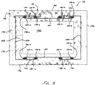
More specifically, with reference to FIGS. 3 and 4, illustrated is a force-
based
sensing device 110 in accordance with one exemplary embodiment. The exemplary
sensing device 110 is shown as comprising a base support 114 having an outer
periphery
118. A plurality of apertures 120, 122, 124, and 126 can be formed in the base
support
114 within the periphery 118. The apertures 120, 122, 124, and 126 can be
located along
the periphery 118 and can circumscribe and define a substantially rectangular
input
portion 150, shown by dashed lines in FIG. 3, that functions as the sensing
portion of the
sensing device 110, as identified above in FIG. 1. The plurality of apertures
can also
define a plurality of isolated beam segments, shown as isolated beam segments
130, 132,
134, and 136, located between the periphery 118 and the corners of the sensing
portion
172, parallel to the sides of the sensing portion 172.
Various sensors may be disposed on or about each isolated beam segment,
respectively. As shown, each isolated beam segment 130, 132, 134, and 136
comprises
two sensors, shown as sensors 138-a and 138-b located on and operable with
isolated
beam segment 130, sensors 140-a and 140-b located on isolated beam segment
132,
sensors 142-a and 142-b located on and operable with isolated beam segment
134, and
sensors 144-a and 144-b located on and operable with isolated beam segment
136. The
particular sensors are configured to detect and measure the force applied to
the sensing
portion 172, or a resulting characteristic thereof, as transferred thereto via
the transfer
elements discussed above and shown in FIGS 1 and 2. In addition, the sensors
are
configured to output an electronic signal, comprising sensor data, through a
transmission
device 146 attached or otherwise related to the sensors, which signal
corresponds to the
applied force as detected by the sensors.
In one exemplary embodiment, the sensors each comprise a strain gage
configured
to measure the strain within or across each of the respective isolated beam
segments.
Moreover, although each isolated beam segment is shown comprising two sensors
located
or disposed thereon, the present invention is not limited to this
configuration. It is
contemplated that one, two or more than two sensors may be disposed along each
of the
isolated beam segments depending upon system constraints and other factors. In
addition,
it is contemplated that the isolated beam segments themselves may be
configured as
sensors. The sensor are discussed in greater detail below.
21
CA 02659647 2009-01-30
WO 2008/016614 PCT/US2007/017127
The transmission device 146 is configured to carry the sensors' output signal
and
sensor data to one or more signal processing devices, shown as signal
processing device
147, wherein the signal processing devices function to process the signal in
one or more
ways for one or more purposes. For example, the signal processing devices may
comprise analog signal processors, such as amplifiers, filters, and analog-to-
digital
converters. In addition, the signal processing devices may comprise a micro-
computer
processor that feeds the processed signal to a computer 148, as shown in FIG.
4. Or, the
signal processing device may comprise the computer 148, itself. Still further,
any
combination of these and other types of signal processing devices may be
incorporated
and utilized. Typical signal processing devices and methods are known in the
art and are
therefore not specifically described herein.
Processing means and methods employed by the signal processing device for
processing the signal for one or more purposes, such as to determine the
coordinates of a
force applied to the force-based touch pad, are also known in the art. Various
processing
means and methods are discussed in further detail below.
With reference again to FIGS. 3 and 4, the base support 114 is shown
comprising
a substantially flat, or planar, pad or plate. The base support 114 can have
an outer
mounting portion 170 and an inner mounting portion 168 that can lie
essentially within
the same plane in a static condition. The outer mounting portion 170 can be
located
between the periphery 118 and the apertures 120, 122, 124, and 126. The inner
mounting
portion 168 can be located between the sensing portion 172 and the apertures
120, 122,
124, and 126. The isolated beam segments 130, 132, 134, and 136 can operably
connect
the inner mounting portion 168 with the outer mounting portion 170. The outer
mounting
portion 170 can be mounted to any suitably stationary mounting structure
configured to
support the sensing device 110, and the projected contacting surface (not
shown) operable
therewith. The sensing portion 172 can be a separate structure mounted to the
inner
mounting portion 168, or it may be configured to be an integral component that
is formed
integrally with the inner mounting portion 168. In the embodiment where the
sensing
portion is a separate structure, one or more components of the sensing portion
can be
configured to be removable from the inner mounting portion. For example, the
sensing
portion 172 may comprise a large aperture formed in the base support 114, and
a
22
CA 02659647 2009-01-30
WO 2008/016614 PCT/US2007/017127
removable force panel configured to be inserted and supported within the
aperture, which
force panel may be configured to receive the applied force as transferred
thereto from
either direction.
The base support 114 can be formed of any suitably inelastic material, such as
a
metal, like aluminum or steel, or it can be formed of a suitably inelastic,
hardened
polymer material, as is known in the art. In addition, the base support 114
may be formed
of glass, ceramics, and other similar materials. The base support 114 can be
shaped and
configured to fit within any type of suitable interface application.
It is noted that the performance of the sensing device 110 may be dependent
upon
the stiffness of the mounting portion, such as the outer mounting portion, of
the base
support 114. As such, the base support 114, or at least appropriate portions
thereof,
should be made to comprise suitable rigidity or stiffhess so as to enable the
sensing
device to function properly, particularly with the transfer and contacting
elements
operable with the sensing device. Altematively, instead of making the base
support 114
stiff, the base support 114, or at least a suitable portion thereof, may be
attached to some
type of rigid support. It is recognized that suitable rigidity functions to
facilitate more
accurate input readings.
The sensing portion 150 can be a substantially flat, or planar, pad or plate
and can
lie within the same plane as the base support 114. The sensing portion 172 can
be
circumscribed by the apertures 120, 122, 124, and 126.
The sensing portion 172 is configured to displace in response to various
stresses
induced in the sensing portion 172 resulting from application of a force
acting on the
contacting portion (not shown) and transmitted to the sensing element. The
sensing
portion 172 is further configured to transmit the stresses induced by the
applied force to
the inner mounting portion 168 and eventually to the isolated beam segments
130, 132,
134, and 136 where resulting strains in the isolated beam segments are induced
and
measured by the one or more sensors.
The base support 114 and sensing portion 172 can have a first side 180 and a
second side 182. The present invention projected force-based input device
advantageously provides for the transfer of force to either the first or
second sides 180
and 182 of the sensing portion 172, and the sensing portion 172 may be
configured to
23
CA 02659647 2009-01-30
WO 2008/016614 PCT/US2007/017127
displace out of the plane of the base support 114 in either direction in
response to the
applied force.
The sensing portion 172 can be formed of any suitably rigid material that can
transfer, or transmit the applied force to the sensors. Such a material can be
metal, glass,
or a hardened polymer, as is known in the art.
The isolated beam segments 130, 132, 134, and 136 can be formed in the base
support 114, and may be defined by the plurality of apertures 120, 122, 124,
and 126.
The isolated beam segments 130, 132, 134, and 136 can lie essentially in the
same plane
as the base support 114 and the sensing portion 172 when in a static
condition. In some
embodiments, the apertures 120, 122, 124, and 126 may be configured to extend
all the
way through the base support 114. For example, the apertures 120, 122, 124,
and 126 can
be through slots or holes. In other embodiments, the isolated beam segments
130, 132,
134 and 136 may be configured to extend only partially through the base
support 114.
As illustrated in FIG. 3, the isolated beam segment 130 can be formed or
defined
by the apertures 122 and 124. Aperture 122 can extend along a portion of the
periphery
118 and have two ends 122-a and 122-b. The aperture 124 can extend along
another
portion of the periphery and have two ends 124-a and 124-b. Portions of the
two
apertures 122 and 124 can overlap and extend along a common portion of the
periphery
118 where one end 122-b of aperture 122 overlaps an end 124-a of aperture 124.
The two
ends 122-b and 124-a, and the portions of the apertures 122 and 124 that
extend along the
common portion of the periphery 118, can be spaced apart on the base support
114 a pre-
determined distance. The portion of the aperture 122 that extends along the
common
portion of the periphery 118 can be closer to the periphery 118 than the
portion of the
aperture 124 that extends along the common portion of the periphery 118. The
area of the
base support 114 between the aperture 122 and the aperture 124, and between
the end
122-b and the end 124-a, can define the isolated beam segment 130.
The isolated beam segments 132, 134, and 136 can be similarly formed and
defined as described above for isolated beam segment 130. Isolated beam
segment 132
can be formed by the area of the base support 114 between the apertures 124
and 126, and
between the ends 124-b and 126-b, respectively. Isolated beam segment 134 can
be
formed by the area of the base support 114 between the apertures 120 and 122,
and
24
CA 02659647 2009-01-30
WO 2008/016614 PCT/US2007/017127
between the ends 120-a and 122-b. Isolated beam segment 136 can be formed by
the area
of the base support 114 between the apertures 120 and 126, and between the
ends 120-b
and 126-a. Thus, all of the isolated beam segments can be defined by the
various
apertures formed within the base support 114. In addition, the isolated beam
segments
may be configured to lie in the same plane as the plane of the sensing portion
172 and
base support 114, as noted above.
The plurality of apertures 120, 122, 124, and 126 can nest within each other,
wherein apertures 122 and 126 extend along the sides 190 and 192,
respectively, of the
rectangular base support 114, and can turn perpendicular to the short sides
190 and 192
and extend along at least a portion of the sides 194 and 196 of the base
support 114.
Apertures 120 and 124 can be located along a portion of the sides 196 and 194,
respectively, of the base support 114 and closer to the sensing portion 172
than apertures
122 and 126. Thus, apertures 120 and 124 can be located or contained within
apertures
122 and 126. Stated differently, the apertures may each comprise a segment
that overlaps
and runs parallel to a segment of another aperture to define an isolated beam
segment,
thus allowing the isolated beam segments to comprise any desired length.
As illustrated in FIG. 5, the isolated beam segment 130 may comprise an outer
or
periphery juncture 154, formed with the outer mounting portion 170, and an
inner
juncture 156, formed with the inner mounting portion 168 of the base support
114. The
inner juncture 156 and outer juncture 154 are configured to receive and
concentrate the
stresses induced on the base support 114 by the applied force to the isolated
beam
segment 130 by deflecting or bending in opposite directions. Upon the transfer
of a force
to the sensing portion 172 from the projected contacting element (not shown),
at least a
portion of the resultant forces are transmitted through or from the sensing
portion 172 to
the isolated beam segment 130 as a result of the configuration of the isolated
beam
segment 130, and specifically the inner and outer junctures 154 and 156, in
relation to the
sensing portion 172 and the inner mounting portion 168. For example, when a
force is
transferred to the sensing portion 172 from the contacting element via the
transfer
element(s), the sensing portion 172 displaces and induces stresses in the
sensing portion
172. A portion of these stresses can be transmitted from the sensing portion
172 to the
inner mounting portion 168, and ultimately to the isolated beam segment 130
where
CA 02659647 2009-01-30
WO 2008/016614 PCT/US2007/017127
sensors 138-a and 138-b function to detect and measure the strain within the
isolated
beam segment 130. It is this measured characteristic or attribute of the
applied force that
the sensor data coinprises. Although not shown in FIG. 5, each of the other
isolated beam
segments (see FIGS. 3 and 4) discussed above function in a similar manner.
With reference again to FIGS. 3 and 4, upon receiving the forces or stresses,
the
isolated beam segments 130, 132, 134, and 136 are configured to deflect in
response to
the displacement of the sensing portion 172 in response to the force being
applied to the
sensing portion 172 as transferred thereto from the contacting element (not
shown).
Thus, the force as transferred and applied to the sensing portion 172 and the
resultant
stresses induced in the sensing portion 172 can be directed to and
concentrated in the
isolated beam segments 130, 132, 134, and 136. The concentrated stresses can
result in
deflection of the isolated beam 130, 132, 134, and 136 segments, and the
deflection can
be measured by the sensors 138-a and 138-b, 140-a and 140-b, 142-a and 142-b,
and 144-
a and 144-b, respectively.
The sensors 138-a and 138-b, 140-a and 140-b, 142-a and 142-b, and 144-a and
144-b can be located along each isolated beam segment 130, 132, 134, and 136,
respectively, essentially in the same plane as the base support 114 and the
sensing portion
172 when in a static condition. Specifically, as shown in FIGS. 3 and 4, a
sensor can be
located at each end of each isolated beam segment. Thus, a sensor 138-a can be
located
on isolated beam segment 130 near the end 124-a of the aperture 124.
Similarly, another
sensor 138-b can be located on the isolated beam segment 130 near the end 122-
b of the
aperture 122. The sensor 140-a can be located on isolated beam segment 132
near
aperture end 126-b of aperture 126, and sensor 140-b can be located on
isolated beam
segment 132 near aperture end 124-b of aperture 124. The sensor 142-a can be
located on
isolated beam segment 134 near aperture end 120-b of aperture 120, and sensor
142-b can
be located on isolated beam segment 134 near aperture end 122-b of aperture
122. The
sensor 144-a can be located on isolated beam segment 136 near aperture end 126-
a of
aperture 126, and sensor 144-b can be located on isolated beam segment 136
near
aperture end 120-b of aperture 120.
The sensors 138-a and 138-b, 140-a and 140-b, 142-a and 142-b, and 144-a and
144-b can also be located along each isolated beam segment 130, 132, 134, and
136 in a
26
CA 02659647 2009-01-30
WO 2008/016614 PCT/US2007/017127
different plane than the base support 114 and the sensing portion 172 when in
a static
condition. The sensors 138-a and 138-b, 140-a and 140-b, 142-a and 142-b, and
144-a
and 144-b do not necessarily have to be in the same plane as the sensing
portion 172, nor
do they have to lie within the same plane with respect to one another. In the
embodiment
shown, the sensors 138-a and 138-b, 140-a and 140-b, 142-a and 142-b, and 144-
a and
144-b do lie within the same, what may be referred to as, sensor or sensing
plane. For
example, an isolated beam segment having a side in the same plane as the
sensing portion
172, and a side in an offset plane from the sensing portion 172 can have the
sensor plane
located on the side that is in the same plane as the sensing portion 172, or
can have the
sensor plane located on the side that is offset to the plane of the sensing
portion 172. In
either case, the sensors are configured to lie within a common sensor plane.
Alternatively, the sensing element may comprise a structure having a non-
planar
configuration, or one with different elevations along its surface. In this
case, the sensors
may lie within different planes with respect to one another, and therefore,
the sensing
element may comprise a number of different sensor planes. The complexity of
the
sensing element and any resulting complexity in the location of the sensors
may be
accounted for in the processing means used to determine the location and
profile of the
applied force.
The sensors 138-a and 138-b, 140-a and 140-b, 142-a and 142-b, and 144-a and
144-b are configured to measure the deflection in the isolated beam segments
130, 132,
134, and 136, respectively, caused by the applied force acting on the sensing
portion 172
as transferred thereto from the contacting element via the transfer
element(s). The
sensors 138-a and 138-b, 140-a and 140-b, 142-a and 142-b, and 144-a and 144-b
can be
any type of sensor capable of measuring properties related to displacement of
the isolated
beam segments 130, 132, 134, and 136. For example, the sensors can be strain
gages,
capacitance gages, liquid level gages, laser level gages, piezo sensors or any
suitable
sensor as is known in the art. The sensors 138-a and 138-b, 140-a and 140-b,
142-a and
142-b, and 144-a and 144-b can generate an electrical signal comprising sensor
data
corresponding to the displacement of the isolated beam segments 130, 132, 134,
and 136.
The electrical signal can be transmitted from the sensors 138-a and 138-b, 140-
a and 140-
b, 142-a and 142-b, and 144-a and 144-b via one or more transmission means.
27
CA 02659647 2009-01-30
WO 2008/016614 PCT/US2007/017127
The transmission means may comprise a wired or wireless transmission means,
including for example, electrical wires 146, such as those shown in FIG. 4, a
radio
transmitter, optical communication devices, and/or others as known in the art.
The
transmission means is configured to carry the signal output by each of the
various sensors
to a signal processor or signal processing means, shown as signal processor
147,
configured to receive and analyze the electrical signal and corresponding
sensor data to
determine the location, profile and/or magnitude of the applied force on the
projected
contacting element and sensing portion 172. The processing means and analysis
methods
can be any known in the art.
FIG. 6 illustrates a force-based sensing device 210 in accordance with still
another
exemplary embodiment of the present invention. In this particular embodiment,
the
sensing device 210 comprises a base support 214 having an outer periphery 218.
A
plurality of apertures 220, 222, 224, and 226 can be formed in the base
support 214
within the periphery 218. The apertures 220, 222, 224, and 226 can be located
along the
periphery 218 and can define a substantially rectangular sensing portion 272
formed
about the periphery 218, as delineated by dashed lines in FIG. 6. The
plurality of
apertures can also define a plurality of isolated beam segments, 230, 232,
234, and 236,
near the corners of, and parallel to the sides of the sensing portion 272,
each of which
may be operable with one or more sensors as shown.
The base support 214 is shown comprising a substantially flat, or planar, pad
or
plate. The base support 214 can have an outer mounting portion 270 and an
inner
mounting portion 268 that can lie essentially within the same plane in a
static condition.
The outer mounting portion 270 can be located between the periphery 218 and
the
apertures 220, 222, 224, and 226, as well as between the input pad 250 and the
various
apertures. In other words, the input pad 250 may be configured to circumscribe
the outer
mounting portion 270. The inner mounting portion 268 can be located inside of
the
various apertures 220, 222, 224, and 226, or in other words be circumscribed
by the
various apertures 220, 222, 224, and 226. The isolated beam segments 230, 232,
234, and
236 can connect the inner mounting portion 268 with the outer mounting portion
270.
The outer mounting portion 270 can be mounted to any suitably stationary
mounting
structure configured to support the sensing device 210. The sensing portion
272 can be a
28
CA 02659647 2009-01-30
WO 2008/016614 PCT/US2007/017127
separate structure mounted to the outer mounting portion 270, or it may be
configured to
be an integral component that is formed integrally with the outer mounting
portion 270.
The sensing portion 272, as supported about and integral with the periphery
218 is
configured to displace in response to various stresses induced in the sensing
portion 272
resulting from application of a force acting on the projected contacting
element (not
shown) and transferred to the sensing portion 272. The sensing portion 272 is
further
configured to transmit the stresses induced by the applied force to the outer
mounting
portion 270 and eventually to the isolated beam segments 230, 232, 234, and
236 where
resulting strains in the isolated beam segments are induced and measured by
the one or
more sensors in a similar manner as described above with respect to the
embodiment
shown in FIG. 3.
Essentially, the sensing device embodiment illustrated in FIG. 6 is similar to
that
shown in FIG. 3, except that the sensing portion 272 of FIG. 6 is located
about the
perimeter or periphery of the sensing device with the inner and outer mounting
portions
being positioned inside or interior to the sensing portion 272. In other
words, the sensing
device of FIG. 6 may be considered to comprise a structural configuration that
is the
inverse of the sensing device shown in FIG. 3. This particular embodiment is
intended to
illustrate that the present invention broadly contemplates some embodiments of
the
sensing device as comprising a first structural element supported in a fixed
position, and a
second structural element operable with the first structural element, wherein
the second
structural element is dynamically supported to be movable with respect to the
first
structural element to define a sensing portion configured to displace under an
applied
force.
With respect to the embodiments shown and others described in the above-
identified patent applications which have been incorporated by reference, the
combination
of providing isolated beam segments, such as isolated beam segments that lie
in or
substantially in the same plane as the sensing portion or modular-type
isolated beam
segments or those that lie in different planes, and configuring the sensing
element to
direct and concentrate the stresses occurring within the sensing portion
to/within the
isolated beam segments, as well as the coplanar or substantially coplanar or
non-planar
relationship of the sensors with the sensing portion, provides significant
advantages over
29
CA 02659647 2009-01-30
WO 2008/016614 PCT/US2007/017127
prior related force-based sensing devices. These advantages include, but are
not limited
to, being able to create the entire sensing device, including the mounting
elements or
portions, from a single piece of material by means of appropriately forming
and locating
the apertures in the material; being able to reduce the sensitivity of the
sensing device to
longitudinal forces or moments transmitted to the sensing portion; being
mechanically
simple; being able to eliminate preload springs; being able to provide a
rugged and robust
design that protects the sensing device from the environment; being able to
minimize size
and weight by making the sensors integral with and coplanar to the sensing
portion; and
being able to register forces from either side of the sensing device.
Furthermore, ceramic
piezoelectric transducers deployed in the more sensitive longitudinal mode
with the strain
applied perpendicular to the axis of the poles and parallel to the electrodes
makes the
sensors more sensitive to elongation or strain and less sensitive to shear and
transverse
forces, thereby reducing the need for elaborate mechanisms to isolate the
transducers
from unwanted forces.
The present invention sensing element may comprise several other embodiments
or other types of force-based sensing devices, some of which may or may not
funetion in
a similar manner as the exemplary force-based sensing devices described above
or
incorporated by reference herein. As such, those discussed or incorporated by
reference
herein are not intended to be limiting in any way. Indeed, it is contemplated
that other
embodiments and other types of sensing elements (e.g., other types of force-
based sensing
devices) will fall within the scope of the present invention that are not
specifically set
forth herein. For example, some additional force-based sensing devices that
may be used
with the present invention projected or elevated contacting element are
described in
United States Patent Nos. 3,657,475 to Peronneau et al.; 4,121,049 to Roeber;
4,340,777
to DeCosta et al.; 4,389,711 to Hotta et al.; 4,511,760 to Garwin et al.; and
4,558,757 to
Mori et al. Still other types of force-based sensing devices are contemplated.
The sensing element 54 may be comprised of any material that provides
sufficient
strength so as to be operable within a particular application, that provides
sufficient
elastic deformation under the forces to be detected by the sensors, and that
provides a
repeatable response under environmental conditions (e.g., force, temperature,
etc.). In the
case of strain gages, this includes many metals (e.g., aluminum, steel,
bronze, etc.), and a
CA 02659647 2009-01-30
WO 2008/016614 PCT/US2007/017127
variety of polymers (e.g., polycarbonate). In the case of piezo sensors, much
less elastic
materials may be used, such as a thicker, tempered steel. Most sensors will be
constructed of metals (due to its high ratio of elasticity to deformation) or
polymers (due
to their inexpensive production costs).
With reference again to FIG. 2, the general projected force-based input device
10
is configured to receive one or more applied forces about the contact surface
18 of the
contacting element 14, which applied forces are shown as forces F. The input
device 10,
and particularly the contacting element 14, may be configured to receive an
applied force
anywhere along its contact surface 18. Alternatively, the contact surface 18
may
comprise a designated input portion or area 26 that may be defmed by one or
more
boundaries, which input portion 26 may be caused to exist anywhere along the
contact
surface 18. In addition, the designated input portion 26 may comprise all or
only a
portion of the area about the contact surface 18.
The contacting element 18, as indicated above, is a projected or elevated
element
with respect to the sensing element 54, which is the element actually
configured to sense
the applied force(s). As such, the projected contacting element 14 is intended
to be
supported in such a projected or elevated position, and to relate to the
sensing element 54
in such a way so as to properly transmit the forces applied to its contact
surface 18 to the
sensing element 54. This is done using one or more transfer elements 94 that
act to both
support the contacting element 14 in a projected position, as well as to
provide a conduit
for the applied forces to be transmitted from the contacting element 14 to the
sensing
element 54 in such a manner so as to provide an accurate measurement of the
force(s)
and/or one or more measurable characteristics thereof. Each of the contacting
element
18, the sensing element 54 and the transfer elements 94 are designed so that
all or
substantially all of the forces are transferred to the sensing element 54.
The transfer elements 94, as coupled to the contacting element 14 and the
sensing
element 54, each comprise a central mounting point and a longitudinal central
axis
extending therethrough. Generally speaking, a force may be applied at any
location on
the contacting element 14, which force may be offset from the central mounting
point and
longitudinal axis of the transfer elements 94. The location of the applied
force with
respect to the location of the transfer elements 94 will affect the resultant
force transferred
31
CA 02659647 2009-01-30
WO 2008/016614 PCT/US2007/017127
to the sensing element 54. As shown in FIG. 2, force F, will induce an inverse
affect on
the contacting element 14, the transfer element 94, and the sensing element 54
as
compared with force F2 due to their relative points of application about the
contacting
element 14 with respect to the location and the longitudinal axis of the
transfer element
94. The forces and the location of the forces as applied are discussed in
greater detail
below.
The present invention projected force-based input device may further comprise
multiple projected contacting elements located in a projected or elevated
position away
from a sensing element, as supported by corresponding transfer elements. As
shown in
FIG. 2 in phantom, the input device 10 compri ses a second projected
contacting element
14-a and corresponding one or more transfer elements 94-a to support the
second
contacting element 14-a. The single sensing element 54 is shown as having
first and
second contacting elements 14 and 14-a, respectively, located in opposing
projected
positions thereabout, with each being supported by one or more transfer
elements. In this
configuration, the sensing element 54 is configured to sense any applied
forces acting on
one or both of the contacting elements and to determine the location and
profile of the
applied forces acting on the various contacting elements. This double-sided
configuration
may be suitable for one or more applications.
As one or more forces are being applied to the contacting element, no matter
the
location of the applied forces about the surface of the contacting element,
the applied
forces are conveyed or transferred to the transfer elements and subsequently
to the
sensing portion of the sensing element as transferred forces where they are
sensed by the
sensor elements in the sensing portion of the sensing element to determine the
location,
profile and/or magnitude of the applied force(s).
The following FIGS. 7-A - 9-B illustrate various exemplary alternative design
embodiments for a projected or elevated force-based input device having one or
more
suitably rigid components. With specific reference to FIGS. 7-A and 7-B,
illustrated are
respective top and side views of a projected or elevated force-based input
device in
accordance with one exemplary embodiment. As shown, the elevated force-based
input
device 310 comprises a projected contacting element 314 supported in a
different
elevation from the sensing element 354. The contacting element 314 is operably
related
32
CA 02659647 2009-01-30
WO 2008/016614 PCT/US2007/017127
to the sensing element 354 via the several transfer elements 394 (shown as
four in
number) configured to support the contacting element 314 in its projected or
elevated
position, as well as to receive and transfer all or substantially all of the
forces acting on or
about the contacting element 314 to the sensing element 354, as discussed
above.
In this particular embodiment, the contacting element 314 comprises a flat,
planar
structure having a rectangular geometric configuration, with its entire
periphery or
perimeter 322 contained within the edges of the sensing element 354 (as viewed
from a
top view). In other words, there is no portion of the cointacting element 314
that extends
beyond the sensing element 354, when observed from the top, as shown in FIG. 7-
A, or
from the side as shown in FIG. 7-B. Furthermore, it is also shown that no
portion of the
contacting element 314 extends beyond the sensing portion 372 of the sensing
element
354, as viewed from the top.
The contacting element 314 is further shown as comprising a cut-out portion
320
having a periphery or perimeter 321. The cut-out region 320 may be any size,
and the
contacting element 314 may comprise any number of cut-outs. The cut-out
portion 320
does not affect those portions of the surface 318 of the contacting element
314 capable of
receiving and registering an applied force. The cutout portion 320 may be used
for a
variety of purposes. For example, the cutout portion may be support a glass or
acrylic
screen for use as a display. The cutout portion 320 may also be used to
facilitate the
mounting of various items to the contacting element 314. In another
application, the
cutout portion may be used to create a "virtual touch" region. In this sense,
forces may be
applied to the contacting element to effectively cause the input device 314 to
register a
touch in a location within the cutout region as if the contacting element
comprised
structure or surface structure in that region. Stated differently, the present
invention may
be configured to average the location of multiple simultaneous applied forces,
such that
the sum of these forces causes the system to register a location at
coordinates within a
cutout region. For example, if a virtual touch was desired to be registered in
the center of
the cutout region 320, multiple simultaneous forces may be applied to the
contact surface
318 of the contacting element 314, which multiple simultaneous forces are
equidistant
from the center of the cutout region, along the same axis, and of the same
magnitude.
The idea behind this being that the input device may be used in applications
requiring a
33
CA 02659647 2009-01-30
WO 2008/016614 PCT/US2007/017127
safety function in order to operate a device (e.g., where two hands are
required to start a
piece of equipment to prevent one hand from being inside the equipment and the
device
inadvertently started).
The sensing element 354 is also shown as comprising a flat, planar structure
having a rectangular geometric configuration. The sensing element 354
comprises a
sensing portion 372 that is configured and that functions in a similar manner
as that
discussed above and described in FIGS. 3-5.
FIGS. 7-A and 7-B further illustrate transfer elements 394 as comprising the
same
length, thus supporting the flat, planar contacting element 314 in an elevated
or projected
plane parallel to that defined by the flat, planar sensing element 354. The
transfer
elements 394 are strategically positioned about the sensing portion 372 of the
sensing
element 354, namely near its edges or perimeter, but such is not required as
the transfer
elements may extend between the contacting and sensing elements at various
positions.
Each transfer element 394 extends upward and contacts the projected contacting
element
314, being coupled to the underside of the contacting element 314 near its
edges or
perimeter 322, so that a majority of applied forces will take place on or
about the surface
of the contacting element 314 at a location within or interior to the transfer
elements 394,
and between the transfer elements 394 and a central axis of the input device
310. More
specifically, the transfer elements 394 are shown as being positioned or
located in each of
the four corners of the contacting element 314.
The transfer elements 394, as configured to transfer forces, are configured
with a
degree of rigidity. In some embodiments, the transfer elements will be more
rigid than in
other embodiments. This may depend upon the particular application, the types
of loads
or forces that will be applied, and other factors. Another factor that may
determine the
needed rigidity of the transfer elements is the distance the projected
contacting element is
to be away from the sensing element, as defined by the height of the transfer
elements
394. Generally speaking, the greater the length of the transfer elements 394
and the
resulting projected height of the contacting element 314 with respect to the
sensing
element 354, the more rigid the transfer elements 394 may need to be in order
to avoid
interference of the contacting or sensing elements with the mounting structure
or another
object (e.g., a partition, such as a wall, trim plate or panel). In essence,
and in most cases,
34
CA 02659647 2009-01-30
WO 2008/016614 PCT/US2007/017127
the transfer elements 394 are intended to be designed so that all or
substantially all of the
applied forces on the contacting element 314 are transferred to the sensing
element 354
via the force transfer elements 394. While the height of the transfer elements
themselves
does not necessarily affect the transfer of forces, their height may
contribute to their
overall flexibility. The particular design or configuration of the transfer
elements 394, as
well as their material makeup, may be determined by those skilled in the art
when
considering the particular application in which the input device 310 will be
used. It has
been discovered that as the contacting element 314 is spaced further from the
sensing
element 354, the sensing element 354 becomes increasingly sensitive to the
components
of the force parallel to the sensing element 354, or off-axis forces (those in
acting along
or within the x-y coordinates or axes or plane of the input device), which
may, in some
cases, impose a practical limit on the separation or projection distance of
the contacting
element 314.
FIG. 7-B further illustrates one or more lighting means or light sources 386
supported between the contacting element 314 and the sensing element 354, and
located
at various locations within the input device. By installing lights between the
contacting
element 314 and the sensing element 354 (or between the contacting element and
a
partition (see FIG. 13)), various aesthetic effects or functional capabilities
may be
realized. The light sources 386 may be any known in the art, such as LED's,
incandescent, fiber optics, light pipes, and others. In addition, the light
sources 386 may
be any color, and can be configured to provide different effects, such as
continuously on,
blinking, strobing, dimming, synchronized with music, etc. The light sources
may be
controlled by a on/off touch region on the contacting element, or by more
traditional
means, such as a physical switch.
As shown, the light sources are mounted to the sensing element 314, but they
could also be mounted to the contacting element 354, the transfer element(s)
394, or any
other structure operating with the input device 310.
With reference to FIG. 8, illustrated is a projected force-based input device
in
accordance with another exemplary embodiment. As shown, the projected force-
based
input device 410 comprises a projected contacting element 414 supported in a
different
elevation from the sensing element 454. The contacting element 414 is operably
related
CA 02659647 2009-01-30
WO 2008/016614 PCT/US2007/017127
to the sensing element 454 via the several transfer elements 494 (shown as
four in
number) configured to support the contacting element 414 in its projected
position, as
well as to receive and transfer all or substantially all of the forces acting
on or about the
contacting element 414 to the sensing element 454, as discussed above.
In this particular embodiment, the contacting element 414 comprises a flat,
planar
structure having an arbitrary geometric configuration, wherein a combination
of
differently curved and straight segments define the perimeter 422 of the
contacting
element 414. The purpose of this particular embodiment is to illustrate that
the contacting
element 414 may comprise any arbitrary shape, as well as to also define a
perimeter that
may be within or without the perimeter of the sensing element (as viewed from
a top
view), or both. As such, the particular arbitrary shape shown in FIG. 8 is not
intended to
be limiting in any way.
FIG. 8 further illustrates various portions of the contacting element 414
extending
beyond the perimeter of the sensing portion 472, as well as the edges or
perimeter of the
sensing element 454. As such, there is provided various portions or segments
of the
surface of the contacting element 414 also extending beyond the sensing
portion 472 and
sensing element 454, which surfaces may receive a force. With the transfer
elements 494
positioned about the edges of the sensing portion 472, or more specifically
substantially
within its corners, and with various portions of the contacting element 414
providing
surface areas that extend beyond the sensing portion 472, it is possible that
the contacting
element 414 may receive forces that are applied between the transfer elements
494 and a
central axis of the input device, as well as forces that are applied between
the perimeter
422 of the contacting element 414 and the transfer elements 494. As such, the
sensing
element 454 is configured to account for the different affects such forces
will have on the
input device 410. Indeed, the contacting element 414 and the input device 410
will
operate even though a portion of the touch receiving surface of the contacting
element
414 extends beyond the sensing element 454. Forces that are applied outside of
the
sensor locations of the sensing element 454 will cause opposing sensors to
respond as if
to a negative force. However, as stated, the processing means may be
configured to
account for such in order to provide accurate results.
36
CA 02659647 2009-01-30
WO 2008/016614 PCT/US2007/017127
Moreover, adequate rigidity within the contacting element and the transfer
elements should be maintained for any portion of the contacting element that
is to receive
a force. The projected distance of the contacting element away from the
sensing element
does not significantly affect the accuracy of the input device for forces
applied
orthogonally to the contacting element. However, the projection distance does
amplify
the effect of any off-axis forces. This amplification is directly related to
the ratio of the
projection distance to the separation distance of the sensors. The larger the
projected
distance of the contacting element relative to the spacing between sensors,
the larger the
amplification of the off-axis forces, and the more potential for error in the
calculated x-y
position of the applied force. However, such may be accounted for
electrically, via
software, mechanical modifications, or any of these in combination.
The sensing element 454 is also shown as comprising a flat, planar structure
having a rectangular geometric configuration, which is configured and
functions in a
similar manner as the sensing element 354 of FIGS 7-A and 7-B. Alternatively,
in other
exemplary embodiments, the sensing element may comprise a configuration having
a
non-planar surface, or a surface with different elevations. In addition, the
sensing
element may comprise a configuration similar to the contacting element shown
in FIG. 8.
Suffice it to say, the present invention contemplates a sensing element, a
projected or
elevated contacting element, and one or more force transfer elements, with
each of these
being able to exist in many different configurations. Although some
configurations may
make the calculations performed by the processing means more difficult, the
input device
can easily be made to operate with the sensing and contacting elements (and
also the
transfer elements) comprising planar or non-planar configurations, as well as
various
arbitrary or other shapes.
FIG. 8 further illustrates transfer elements 494, which are also configured
and
function in a similar manner as the transfer elements of FIGS. 7-A and 7-B,
namely to
support the flat, planar contacting element 414 in an elevated or projected
plane parallel
to that defined by the flat, planar sensing element 454.
FIGS. 9-A and 9-B illustrate a projected force-based input device in
accordance
with another exemplary embodiment. As shown, the projected force-based input
device
510 comprises a projected contacting element 514 supported in a different
elevation from
37
CA 02659647 2009-01-30
WO 2008/016614 PCT/US2007/017127
the sensing element 554. The contacting element 514 is operably related to the
sensing
element 554 via the several transfer elements 594 (shown as four in number)
configured
to support the contacting element 514 in its projected position, as well as to
receive and
transfer all or substantially all of the forces acting on or about the
contacting element 514
to the sensing element 554, as discussed above.
In this particular embodiment, the contacting element 514 comprises a
contoured,
nonpianar structure having a multi-elevational, frustroconical geometric
configuration, as
viewed from the top, with a portion of its periphery or perimeter 522
contained within the
edges of the sensing element 554 (as viewed from the top) and a portion
extending
beyond the edges of the sensing element 554, as shown. This embodiment also
illustrates
the ability to provide a contacting element that is comprised of different
topographical
elevations. As such, the particular design shown in FIGS. 9-A and 9-B is not
intended to
be limiting in any way. To the contrary, as will be recognized by those
skilled in the art,
the contacting element 514 may comprise any number of elevational changes,
particularly
along its upper contact or force receiving surface. In addition, an embodiment
comprising a contoured surface may further comprise any geometric
configuration.
The sensing element 554 is shown as comprising a similar configuration as that
of
FIGS. 7-8. As in other embodiments, the sensing element 554 comprises a
sensing
portion 572 that is configured and that functions in a similar manner as that
discussed '
above and described in FIGS. 3-5.
FIGS. 9-A and 9-B further illustrate transfer elements 594 as comprising
different
lengths, thus supporting the contoured contacting element 514 in an elevated
or projected
position relative to the flat, planar sensing element 554. Different lengths
are provided in
order to account for the nonplanar configuration and the various elevations
formed in the
contacting element 514. Nonetheless, the transfer elements 594 are configured
to provide
the same function as otherwise discussed herein. If needed, the processing
means may be
configured to account for the nonplanar configuration. However, the
calculations to
determine the location, profile and/or magnitude of the forces being applied
to the
contacting element 514 may or may not be more complex.
The transfer elements 594 are strategically positioned about the sensing
portion
572 of the sensing element 554, namely near its edges or perimeter. Likewise,
each
38
CA 02659647 2009-01-30
WO 2008/016614 PCT/US2007/017127
transfer element 594 extends upward and contacts the projected contacting
element 514,
being coupled to the underside of the contacting element 514 near its edges or
perimeter
522. With the contacting element 514 so configured, some of the applied forces
will take
place on or about the surface of the contacting element 514 within or interior
to the
transfer elements 594, and between the transfer elements 594 and a central
axis while
some of the applied forces will occur between the perimeter 522 and the
transfer elements
594.
Despite the multi-elevational configuration of the contacting element 514,
normal
z-axis forces will be transferred to the sensing element 554 much the same way
they are
with a flat, planar contacting element. The non-planar, multi-elevational
contacting
element may tend to produce a higher ratio of off-axis (x-y) forces to on-axis
(z-axis)
forces that may have to be accounted for and accommodated either mechanically,
electrically or with software, or any combination of these. However, the
normal forces
will translate properly and the input device may be made to function with a
contacting
element having such a configuration.
FIGS. 10-A and 10-B illustrate a projected force-based =input device 610 in
accordance with another exemplary embodiment. As shown, the projected force-
based
input device 610 comprises a contacting element 614 operably coupled and
related to a
sensing element 654 in a projected position, having a height h, via transfer
elements 694.
This embodiment is similar in form and function to the one described above and
shown in
FIGS. 3-5, but with some differences. As such, every feature and function is
not set forth.
The contacting element 614 comprises an upper contacting surface 618
configured
to receive a force applied thereto. The contacting element 614 is shown as a
plate-like
structure having a uniform thickness. The contacting element 614 may be formed
of
many different materials, including, but not limited to, glass, marble, stone,
ceramic,
steel, plastic, and others. In addition, also as described above, the
contacting element 614
may comprise different sizes and shapes.
The sensing element 654 comprises a plurality of apertures, shown as apertures
630 and 632, which extend through the sensing element 654, and which function
to create
and define a plurality of isolated beam segments within the sensing element
654, only one
of which is shown, namely isolated beam segment 634. The isolated beam segment
634
39
CA 02659647 2009-01-30
WO 2008/016614 PCT/US2007/017127
is shown as being positioned or oriented on an incline where it is located
diagonally with
respect to the perimeter 662 of the sensing portion 654. The sensing element
654
comprises additional isolated beam segments (not shown) situated in a similar
manner.
Each of these isolated beam segments contain one or more sensors, or are
comprised of
sensing material. The funetion of these isolated beam segments and any sensors
located
thereon is taught above.
The apertures 630 and 632, as well as the mounting portion 666 and movable
component 638 further define a sensing portion 672 configured to receive the
applied
forces acting on the contacting element 614 as transferred to the sensing
portion 672
. through the transfer elements 694. The transfer element 694 comprises a
first end 696
securely coupled to the underside of the contacting element 614, and a second
end 698
that is securely coupled to the sensing element 654 via fasteners 644, which
may be bolts,
screws, etc. The transfer element, as well as those not shown, are each
coupled to the
sensing element 654 at a location within the sensing portion 672.
The sensing element 654 may be mounted via mounting portion 666, which
consists of an inner mounting portion 668 and an outer mounting portion 670.
The
mounting portion 666 may be securely coupled to any structure capable of
supporting the
projected force-based input device 610. For example, the mounting portion 666
may be
securely mounted to the partition 650.
FIG. 10-B further illustrates an optional partition 650 in the form of a trim
plate
(not shown in FIG. 10-A for clarity) that may be used for aesthetic purposes
to hide or
conceal the sensing element 654 as mounted in its intended position about a
structure.
The partition 650 may also be functional in that it may facilitate mounting of
the sensing
element 654. The partition 650 may be located at any point between the
contacting
element 614 and the sensing element 654, and may comprise any size,
configuration,
color, etc. The partition 650 comprises apertures through which the transfer
elements 694
may extend. However, the partition 650 is preferably configured to not
interfere with the
function of either the contacting element, the transfer elements or the
sensing element.
FIG. 10-B further illustrates the sensing element 654 as comprising a
protruded
member 640 extending upward from the sensing element 654 about its perimeter.
The
protruded member is configured to support the partition 650 in an offset
position so that
CA 02659647 2009-01-30
WO 2008/016614 PCT/US2007/017127
no part of the partition 650 is allowed to contact the sensing element 654,
which may
skew the transfer of forces and/or any readings by the sensors, thus
interfering with the
accuracy of the projected force-based input device 610.
With reference to FIGS. 11-A and 11-B, shown is a projected force-based input
device 710 in accordance with yet another exemplary embodiment of the present
invention. In this embodiment, the projected force-based input device 710
comprises a
floating design, wherein the components of the input device 710 are all
supported in an
elevated manner via a support 738 coupled to the mounting portion 766 of the
sensing
element 754. The mounting portion 766 extends around the perimeter of the
sensing
element 754, but may be located elsewhere on the sensing element 754. The
support 738
further extends upward from the top surface of the sensing element 754 to
operably
support a trim plate 750.
The contacting element 714, with its upper contact surface 718, is located in
a
projected position and is operably related to the sensing element 754 via
transfer elements
(e.g., transfer element 794), which is secured within the sensing portion 772
of the
sensing element 754 via a fastener 744 having a nut 746. In this particular
embodiment,
the transfer element 794 is concealed within a decorative shroud or cover 776
having a
decorative cap 778. The contacting element 714 and sensing element 754
function in a
similar manner as described elsewhere herein, wherein the sensors (e.g.,
sensor 784) are
configured to measure the force as transferred by the transfer elements from
the
contacting element 714 to the sensing portion 772 of the sensing element 754.
The projected force-based input device 710 further comprises a gasket 780
retained by a retainer 782. The gasket 780 is positioned adjacent the
underside of the trim
plate 750 and is held in place against the trim plate 750 by a gasket retainer
782. The
gasket 780 functions as a seal to ensure any moisture, rain, dust, dirt, other
contaminants,
etc. in the environment in which the input device is used is kept out of the
interior of the
input device where the sensors, the sensing portion, and the various
electronics are
supported. The gasket 780 may comprise a washer, and should be flexible enough
so as
to not absorb a significant amount of the applied force. Alternatively, all
gaskets in a
given design should be configured to absorb an equal percentage of the applied
force.
41
CA 02659647 2009-01-30
WO 2008/016614 PCT/US2007/017127
FIGS. 12-A and 12-B illustrate a projected force-based input device 810 in
accordance with still another exemplary embodiment of the present invention.
In this
particular embodiment, the construction and design of the various components
of the
input device 810 are similar to those described above and illustrated in FIGS.
10-A and
10-B, with some notable differences.
One difference between the exemplary input device 610 illustrated in FIGS. 12-
A
and 12-B as opposed to the exemplary input device 810 illustrated in FIGS. 10-
A and 10-
B is the elimination of the dedicated, separate transfer elements from the
input device
810. Instead, the input device 810 comprises a protruded portion 840
integrally formed
with the sensing element 854, which extends upward from the sensing element
854. In
the embodiment shown, the protruded portion 840 is located about the perimeter
of the
sensing element 854, but this is not intended to be limiting in any way. The
protruded
portion 840 is configured to operably relate the contacting element 814 to the
sensing
element 854. In other words, the protruded portion 840 functions to transfer
the forces
applied to the contacting element 814 to the sensing element 854 much the same
way the
individual transfer elements do in other described embodiments. In this case,
the forces
are transferred to the outer portion of the sensing element 854. As such, the
sensing
portion 872 of the sensing element 854 is defined as that part of the sensing
element 854
that is without or exterior to the apertures (e.g., apertures 830 and 832). In
addition, the
resultant location of the mounting portion 866 is interior to or within the
apertures of the
input device 810. Indeed, the mounting portion 866 is shown attached or
coupled to the
structure 838, which extends between each of the apertures of the input device
810.
The protruded portion may be comprised of the same or different'material, but
should be sufficiently stiff or rigid so as to effectively transfer the forces
from the
contacting element 814 to the sensing element 854, and to ensure proper
operation of the
input device as described above.
FIG. 13 illustrates projected force-based input device 910 as comprising a
contacting element 914 operably related to a sensing element 954 in a
projected manner,
as supported by a transfer element 994. In this particular embodiment, the
input device
910 is shown as passing through a partition 906, such as a wall, trim plate,
etc., which
may be functional (e.g., utilitarian) or nonfunctional (aesthetic) or both.
The partition 906
42
CA 02659647 2009-01-30
WO 2008/016614 PCT/US2007/017127
may be formed or modified to receive the transfer elements 994 therethrough,
thus
allowing the contacting element 914 to still be projected from the sensing
element 954,
but also to maintain and conceal the sensing element 954 behind the partition
906.
If desired, or if needed, the partition 906 may be sealed with a sealing
means, such
as the rubber diaphragm 908 shown in FIG. 13. The sealing means may extend
between
the transfer element 994 and the partition 906, thus sealing the sensing
element 954 from
the environment in which the contacting element 914 is located. This may be
advantageous for those applications in which the contacting element may be
subjected to
harsh or wet operating conditions, where it would be desirable to further
protect the
sensing element from such conditions. The sealing means may comprise other
types and
materials as commonly known in the art.
FIG. 14 illustrates a projected force-based input device in accordance with
another
exemplary embodiment of the present invention. As shown, the force-based input
device
1010 comprises a contacting element 1014 supported in a projected manner and
related to
a sensing element 1054 in a similar manner as discussed herein. However, the
transfer
elements 1094 supporting the contacting element are comprised of compression
springs,
made from high aspect ratio rectangular wire so that they are not easily
displaced or bent
in the x-y direction, but are sufficiently rigid so as to transfer a force in
the z-direction.
With reference to FIGS. 15-A and 15-B, illustrated is a projected force-based
input device formed in accordance with still another exemplary embodiment of
the
present invention. As shown, the input device 1110 comprises a flat, planar
sensing
element 1154, and a plurality of individual elevated or projected contacting
elements,
shown as contacting elements 1114-a, 1114-b and 1114-c, each being connected
by
corresponding transfer elements, namely 1194-a, 1194-b and 1194-c,
respectively. Also
shown are sensors 113 8 supported within the sensing element 1154, which
sensors detect
and measure forces applied to any one of the multiple contacting elements
1114.
This particular embodiment illustrates several different concepts at work
within a
single input device. First, multiple projected or elevated contacting elements
are
supported about and operable with a single sensing element, which multiple
contacting
elements are physically independent of one another. Second, projected or
elevated
contacting elements may be coupled to either side of the sensing element, with
the input
43
CA 02659647 2009-01-30
WO 2008/016614 PCT/US2007/017127
device operable to detect a force being applied to either of the contacting
elements on
either side of the sensing element. Third, multiple transfer elements are
shown relating
the multiple contacting elements to the sensing element, which multiple
transfer elements
are located at different locations. Fourth, the elevated contacting elements
may be
configured at different orientations with respect to one another and the
sensing element.
In addition, the transfer elements operable with the contacting elements may
be of a
different size.
Multiple elevated contacting elements supported on opposite sides of the same
sensing element functions to generate inverse measurements. Indeed, a force
applied on
contacting element 1114-a will create a measurement that is inverse to the
same force
applied on the contacting element 1114-c. However, the inverse nature of the
signals will
be largely irrelevant with respect to processing the signals, determining the
location and
profile of the applied forces about the various contacting elements, and
registering these
locations to cause the input device to perform the intended functions.
FIG. 15-B further illustrates multiple contacting elements about one another.
Specifically, input device 1110 comprises a contacting element 1114-d
supported about
the contacting element 1114-a. In this configuration, any forces applied to
the contacting
surface of the contacting element 11 14-d are projected onto the sensing
element 1154 via
the transfer elements 1 194-d, the contacting surface 111 g-a, and the
transfer elements
1194-a, just as if the applied force were occurring directly on the sensing
element 1154.
As such, the input device of the present invention may comprise multiple
elevated or
projected contacting elements supported about one another, keeping in mind
that
sufficient rigidity should be maintained to permit proper operation and force
transfer.
With reference to FIG. 16, illustrated is a projected force-based input device
in
accordance with still another exemplary embodiment of the present invention.
The input
device 1210 comprises a flat, planar projected or elevated contacting element
1214 and a
flat, planar sensing element 1254 configured as any of the sensing elements
discusses
herein. In this particular embodiment there are no transfer elements as the
contacting
element 1214 is supported directly about the sensing element 1254. The
contacting
element 1214 is sized and configured to fit within or to be contained within
the sensing
portion 1272 of the sensing element 1254 such that a force applied to any part
of the
44
CA 02659647 2009-01-30
WO 2008/016614 PCT/US2007/017127
contacting surface 1218 of the contacting element 1214 will register a force
detectable by
the sensing element 1254. In this configuration, any forces acting on the
contacting
element 1214 are transferred to the sensing element 1254 via the contacting
element
1214. The overall effect is the same as if transfer elements were present.
This particular
embodiment may be useful in applications in which a more low-profile design is
needed,
or if it is not practical to use transfer elements. It is noted that the
thickness of the
contacting element 1214 may be any thickness.
Alternative to that shown, the contacting element may comprise a size and
shape
defining a perimeter that extends outside or beyond the sensing portion 1272.
In this
case, whatever mounting or other structures or objects are to be configured
and positioned
so as to not interfere with the contacting or sensing elements, similar to the
other
embodiments discussed herein.
FIG. 17 illustrates a projected force-based input device in accordance with
still
another exemplary embodiment of the present invention. In this configuration,
the input
device 1310 comprises a projected or elevated contacting element 1314
supported from a
sensing element 1354 via transfer elements 1394. Unlike the other embodiments
discussed herein, the sensing element 1354 is shown as having a cut-out
portion 1320
formed therein to allow a force Fl to be applied to a contacting surface 1318
of the
contacting element 1314, which contacting surface 1318 is proximate the
sensing element
1354 rather than distal. As such, the sensing element 1354 detects and
registers a tension
(-z) force rather than a compression (+z) force. However, this is accounted
for by
processing means operable with the input device to receive the signals output
by the
various sensors in the sensing element.
As indicated elsewhere herein, the input devices of the present invention may
be
configured to operate with forces acting on either side of the contacting
element and the
sensing element, or both. In other words, each of the contacting and sensing
elements
may be configured to receive an applied force from either side, which forces
are
detectable and measurable by the sensors supported within the sensing element.
This is
shown herein by the contacting element 1314 having forces Fl and F2 applied
thereto on
respective opposing sides or surfaces. The cut-out 1320 is illustrated in
phantom view as
it is conceivable that the sensing element 1354 may comprise multiple sensing
elements
CA 02659647 2009-01-30
WO 2008/016614 PCT/US2007/017127
not coupled together, but each operable within the same input device to
support different
portions of the elevated contacting element 1314.
FIG. 18 illustrates another exemplary projected force-based input device 1410,
wherein the transfer elements 1494 relating the sensing element 1454 to the
elevated or
projected contacting element 1414 are supported on an incline with respect to
the
contacting element 1414 or sensing element 1454 or both. This may be due to
design
constraints, such as a partition 1406 that requires transfer elements oriented
other than
perpendicular or orthogonal to the sensing or contacting elements. FIG. 18
further
illustrates means for sealing the transfer element with respect to the
partition 1406, which
means for sealing is shown as comprising a rubber gasket 1408.
FIGS. 19-A and 19-B illustrate a projected input device 1510 formed in
accordance with still another exemplary embodiment. In this embodiment, the
input
device 1510 comprises a projected or elevated contacting element 1514
supported about a
sensing element 1554 having a non-planar, multi-elevational configuration. The
sensing
element 1554 comprises multiple sensors (not shown) that are operable to sense
a force
acting on the contacting element 1514 and transferred to the sensing portion
1572 of the
sensing element 1554 via transfer elements 1594. The transfer elements 1594
are shown
as comprising different sizes in order to support the projected or elevated
contacting
element 1514 in a horizontally oriented position, and to conform to the
multiple
elevations of the sensing element 1554. This embodiment illustrates that,
similar to the
contacting element, the sensing element may comprise a shape and configuration
other
than simply a flat, planar configuration. As the size of the transfer elements
has no
bearing on the transfer of forces from the contacting element to the sensing
element, this
particular input device embodiment functions similar to that shown in FIG. 1.
FIG. 20 illustrates a top view of a projected force-based input device 1610
having
an exemplary user interface layout. It is noted that the layout may be
configured in any
way desired to provide many different types of user interfaces. In addition,
the input
device 1610 may be configured to function in any manner as set forth above
with respect
to any of the several embodiments discussed herein. Different user interfaces
are
described in copending United States Provisional Application No. 60/ 931,400,
filed May
22, 2007, and entitled, "User Interfaces Operable with a Force-Based Input
Device"
46
CA 02659647 2009-01-30
WO 2008/016614 PCT/US2007/017127
(Attorney Docket No. 02089-32356.PROV, which is hereby incorporated by
reference.
Types of interfaces include, but are not limited to, tactile buttons, non-
tactile buttons,
visual paints or adhesives, removable objects, engravings, static attachments
and/or
dynamic attachments.
As shown, the contacting element 1614, or rather the upper contact surface
1618
of the contacting element 1614, comprises a plurality of delineated areas or
regions, each
having one or more identifying indicia, whereupon a force acting on the
contacting
element 1614 within any one of these regions would cause the input device 1610
to
execute a pre-determined or designated function. More specifically, in the
embodiment
shown, the contacting element 1614 comprises a sort of keypad 1663 having a
plurality of
input regions or keys representing a plurality of numbers. It is noted that
each of the
various keys of the keypad 1663 are not mechanical buttons, but simply input
areas to be
touched that are delineated on the contacting element 1614. Each key is
defined by its
location on the contacting element 1614, such that when a touch occurs within
that region
or key the input device performs the desired=fixnction.
The contacting element 1614 may comprise any number of defined input regions
or areas, such as the group of input regions 1665 that may be used to control
one or more
additional functions. These input regions are configured to receive a force,
which forces
are then transferred to the sensing portion 1672 of the sensing element 1654.
The sensing
portion 1672 is defined by the location of the various transfer elements 1694,
the
apertures 1630 and 1632 (which define the isolated beam segments, such as beam
segment 1634), and the mounting portion 1666 (which in this case is an outer
mounting
portion extending around the perimeter of the sensing portion 1654).
The input device 1610 is shown as further comprising a display screen 1671 and
a
speaker 1677. These are designed to be operable with corresponding holes or
cutouts (not
shown, but existing) in the contacting element 1614. The display 1671 may be a
separate
device mounted to the underside of the contacting element 1614, or it may be
integrally
formed with the contacting element 1614 (e.g., glass or acrylic). As such, the
display
1671 may also comprise any number of input regions that are configured to
receive and
register a touch or force input to cause the input device 1610 to perform a
designated
function. Indeed, with the display located within the sensing portion 1672 of
the input
47
CA 02659647 2009-01-30
WO 2008/016614 PCT/US2007/017127
device 1610, and with the display 1671 being coupled to or integrally formed
with the
contacting element 1614, the display is capable of comprising one or more
defined input
regions.
It is specifically noted herein that the contacting element 1614 comprises
several
holes or apertures formed in its surface. These are intended to provide the
input device
with added functionality. However, these holes or apertures have no affect on
the
operation of the input device. In other words, the contacting element in this
or any of the
other embodiments discussed herein may comprise various holes, cutouts,
recesses, etc.
formed in or about its surface that do not affect the other portions of the
contacting
element. Indeed, a touch or applied force at a given location on a contacting
element with
no holes or cutouts would register the same as a touch or applied force at a
respective
given location on a contacting element of the same size and configuration,
except with
one or more holes formed therein. To illustrate, with respect to the exemplary
input
device 1610 of FIG. 14, a force applied at the location on the contacting
element
delineated by the number 3 (the number 3 key) would register the same no
matter if the
contacting element 1614 had a cutout or not for a display 1671. In essence, an
elevated or
projected contacting element of the present invention may comprise any number
of holes
or cutout regions, without affecting the operation of the input device to
detect forces
applied about the actual surface regions of the contacting element.
It is noted herein that each of the above-described embodiments of input
devices
may comprise similar components and functions as any other embodiment, as
applicable
and recognized by those skilled in the art. Indeed, some components described
specifically in some embodiments, and their functions, may operate with the
input devices
of other embodiments, as appropriate, and as will be recognized by those
skilled in the
art. As it was not necessary, each embodiment was not specifically set forth
in complete
detail, only how they differed from one another. However, each of the
embodiments is
based upon and comprises many of the same functions as the input device shown
and
described in FIGS. 1-5, which description is intended to be incorporated into
each of the
additional embodiments, as appropriate.
PROCESSING MEANS
48
CA 02659647 2009-01-30
WO 2008/016614 PCT/US2007/017127
As indicated above, the present invention projected force-based input device
may
comprise one or more sensors configured to output a data signal that may be
used to
facilitate the determination of a location and profile of the applied force
about the
contacting element. Based on this, it is contemplated that the present
invention further
comprises one or more processing means that may receive and utilize the data
signals
output by the sensors and perform various processing steps to determine the
location or
coordinates of the applied forces acting on the contacting element for one or
more
purposes.
The method for calculating the location, profile and/or magnitude of an
applied
force acting on the contacting element is the same as for an input device
having a non-
projected contacting element. Any amplification of the x-y forces induced by
the
projected distance is inherently minimized by the sensing portion, and what is
not
minimized is inherently read by the sensors and induces some error in the x-y
position
just as an off-axis force on the non-projected contacting element is minimized
by the
sensing portion. Again, the location, number, size and methods of construction
of the
transfer elements have no effect on the calculation of the applied force
location, as long as
the input device is sufficiently rigid. In addition, the projection distance
has no effect on
the method of calculation of the applied force location, although, as noted
above, this may
affect the overall accuracy of the applied force location if the flexibility
of the transfer
elements is capable of permitting interference of either the contacting or
sensing element
with one or more structures or objects.
Exemplary techniques for processing signals from the sensors are also
disclosed in
commonly owned co-pending U.S. Patent Application Serial No. 11/402,985, filed
April
11, 2006, and entitled "Sensor Signal Conditioning in a Force-Based Input
Device"
(attorney docket 24415.NP1), and U.S. Patent Application Serial No.
11/402,692, filed
April 11, 2006, and entitled "Sensor Baseline Compensation in a Force-Based
Touch
Device" (attorney docket 24415.NP2), each of which are incorporated herein by
reference
in their entirety.
Indeed, other processing means and methods may be employed by the present
invention that are known to those skilled in the art. For example, United
States Patent
Nos. 4,121,049 to Roeber; and 4,340,772 to DeCosta et al. disclose and discuss
49
CA 02659647 2009-01-30
WO 2008/016614 PCT/US2007/017127
exemplary processing methods. As such, the present invention should not be
limited to
any particular processing means or methods, as each of these is contemplated
for use and
may be implemented with the force-based touch pad of the present invention to
perform
its intended function of processing the signal(s) received from the various
sensors for one
or more.purposes.
The foregoing detailed description describes the invention with reference to
specific exemplary embodiments. However, it will be appreciated that various
modifications and changes can be made without departing from the scope of the
present
invention as set forth in the appended claims. The detailed description and
accompanying
drawings are to be regarded as merely illustrative, rather than as
restrictive, and all such
modifications or changes, if any, are intended to fall within the scope of the
present
invention as described and set forth herein.
More specifically, while illustrative exemplary embodiments of the invention
have
been described herein, the present invention is not limited to these
embodiments, but
includes any and all embodiments having modifications, omissions, combinations
(e.g., of
aspects across various embodiments), adaptations and/or alterations as would
be
appreciated by those skilled in the art based on the foregoing detailed
description. The
limitations in the claims are to be interpreted broadly based on the language
employed in
the claims and not limited to examples described in the foregoing detailed
description or
during the prosecution of the application, which examples are to be construed
as non-
exclusive. For example, in the present disclosure, the term "preferably" is
non-exclusive
where it is intended to mean "preferably, but not limited to." Any steps
recited in any
method or process claims may be executed in any order and are not limited to
the order
presented in the claims. Means-plus-function or step-plus-function limitations
will only
be employed where for a specific claim limitation all of the following
conditions are
present in that limitation: a) "means for" or "step for" is expressly recited;
and b) a
corresponding function is expressly recited. The structure, material or acts
that support
the means-plus function are expressly recited in the description herein.
Accordingly, the
scope of the invention should be determined solely by the appended claims and
their legal
equivalents, rather than by the descriptions and examples given above.
What is claimed and desired to be secured by Letters Patent is: