Note: Descriptions are shown in the official language in which they were submitted.
CA 02659674 2009-01-30
WO 2008/115258 PCT/US2007/074864
1
Multifunctional Nanoscopy for Imaging Cells
Cross-Reference and Priority Claim to Related Patent Application:
This patent application claims priority to U.S. provisional patent application
60/821,040, filed August 1, 2006, and entitled "Multifunctional Nanoscopy for
Imaging Cells", the entire disclosure of which is incorporated herein by
reference.
Statement Regarding Federally Sponsored Research or Development:
This invention was made with government support under NIH grants such as
EB002168, HL042950, and CO-27031 awarded by the National Institutes of Health
(NIH). The government may have certain rights in the invention
Field of the Invention:
The field of this invention relates generally to techniques for measuring
characteristics of an object (such as the cell function and structure of one
or more
living cells) on a nanoscale via an array of integrated nanosensors that are
responsive
to various perturbations such as acoustic waves, light, or electric charge.
Background and Summary of the Invention:
The rapid acquisition and analysis of high volumes of data in biological
samples had its advent in the early days of the human genome sequencing
project.
Microarray technology has facilitated the interrogation of large numbers of
samples
for biologically relevant patterns in a variety of physiological, drug-induced
or
clinically relevant cellular states. A challenge has now presented itself with
respect
to how these large volumes of information can be integrated into an accurate
model
of cellular behavior and processes. For example, information relating the
effect of a
drug to the extent and duration of apoptosis in cancer cells would be
invaluable
information in a screen for cancer drugs. Similarly, information of
cytoskeletal
changes leading to invasiveness would greatly streamline the development of an
efficient anti-angiogenic drug strategy.
The discipline of cytomics has emerged to meet these and other demands in
both the academic and industrial research communities. The importance of
cytomics derives from the fact that the cell is the minimal functional unit
within
CA 02659674 2009-01-30
WO 2008/115258 PCT/US2007/074864
2
our physiology. An attendant technology to the emergence of cytomics is High
Content Screening (HCS) which is generally defined as a simultaneous, or near
real-
time, multiparametric analysis of various aspects of cell state.
The complexity of cell function is only part of why cytomics will likely
become a major field of study in the near future. Every cell is different, and
by
studying each cell's unique function, that cell type can be further modeled
for
subsequent analysis using statistical techniques. Within a short time, the
inventors
herein forecast that most pharmaceutical companies will not operate without
encompassing the essential features of cytomics-drugs-design; a process that
will
increasingly operate at the level of modified cellular functions. Future
cancer
strategies may place greater emphasis on cytome-alignment or cytomic-
realignment,
which may be viewed as the "cellular form" of tissue engineering. Such an
approach
will require a better-than-ever understanding of how the cell operates, of how
to
measure cell function, and of how to characterize a live cell in minute
detail. To
meet this challenge, there is need in the art for the development of new
technologies
and new analytical tools for exquisitely sensitive single-cell analysis.
A primary goal of cytomics is the discovery of functional relationships
between the cell (cytome) and the metabolic pathways (i.e., proteomics, which
enables rapid identification of proteins from specific cell populations)
resulting from
genetic control mechanisms (i.e., genomics; some in the art relate cytomics to
functional genomics). With cytomics, the amount of information being collected
from the cell is expanded in order to obtain functional data, not just
morphological,
phenotypic, or genotypic data.
Currently, there are two major branches of cytomics: analytical cytology and
image cytology. The first, analytical cytology, is comprised of traditional
analytical
techniques such as: flow cytometry, single cell analysis systems and tissue
analysis
(after cell separation). The second, image cytology (and analysis) is
comprised of
techniques such as "quantitative" fluorescence assays, high throughput cell
culture
assays (96-384-1536 well plates), drug effect assays of cytotoxicity,
toxicology assays,
apoptosis assays, cell proliferation assays, cell ploidy assays, and DNA array
assays.
These techniques are typically applied to single cells, tissues and sections,
and cell
culture systems in both 3D and 4D cell culture environments. Laser Scanning
Cytometry (LSC) is a well-known example of this type of assay.
CA 02659674 2009-01-30
WO 2008/115258 PCT/US2007/074864
3
At the highest level, cytomics links technology to functional biology at the
cellular level by relating measurement and detection to structure and
function. To
achieve this end, cytomics integrates tools like flow cytometry, image
cytometry, etc.
with proteomics and this brings together traditional cytometry and non-
traditional
cytometry. With the application of so many different measurement technologies
to
the same problem, informatics now assumes a primary rather than a secondary
role
in cytomics. For instance, in a typical flow cytometry system, there are
120,000
events per second per output channel, with measurements being acquired for
multiple channels. Another example is offered by very high speed cell culture
plate
imaging systems applied to detect fluorescent markers in cells.
The term HCS is used to differentiate assays that use live cells and to
provide
single point readouts (e.g., High Throughput Screening (HTS) assays), which
are
often based on the biochemistry of ligand binding. HCS combines cell-based
arrays
with robotics, informatics, and advanced imaging to provide richly detailed
information on cell morphology and other responses in large quantities.
Many protocols for generating data are already well developed in their
respective disciplines, from quantitative Polymerase Chain Reaction (PCR), to
flow
cytometry, to antibody staining. The methods for acquisition of this data,
such as
different types of optical microscopy, have already undergone extensive
development.
Perhaps the most important image acquisition methods for HCS relate to
cellular
imaging, including drug effect assays for cytotoxicity, apoptosis, cell
proliferation,
and nucleocytoplasmic transport. Frequently, these approaches utilize cell
sensors
based on fluorescent proteins and dyes, and thus provide researchers with an
ability
to screen drugs and to answer more complex biological questions such as target
identification and validation and to investigate gene and protein function.
In an effort to fill a need in the art for improved cellular imaging
techniques,
the inventors herein disclose a new, inexpensive, and easy-to-use imaging
technology suitable for simultaneous capture of multiple measurements from
individual cells that will enable molecular colocalization, metabolic state
and
motility assessment, and determination of cell cycle, texture, and morphology.
This
technology will be capable of not only HCS, but also permit selection of
single cells
for subsequent high-resolution imaging based on the outputs of the HCS. By
increasing the analytical resolution to assess the sub-cellular state in vivo,
the
inventors herein hope to increase biological resolution by providing a means
to
CA 02659674 2009-01-30
WO 2008/115258 PCT/US2007/074864
4
follow the location, timing, and interdependence of biological events within
cells in a
culture.
The present invention builds upon the previous works by one of the
inventors herein, wherein the extraordinary magnetoresistance (EMR) and
extraordinary piezoconductance (EPC) properties of hybrid semiconductor/metal
devices were used to develop improved sensing techniques for a wide variety of
applications. For EMR devices, examples include but are not limited to read
heads
for ultra high density magnetic recording, position and rotation sensors for
machine
tools, aircraft and automobiles, flip phone switches, elevator control
switches, helical
launchers for projectiles and spacecraft, and the like. For EPC devices,
examples
includes but are not limited to a myriad of pressure sensors, blood pressure
monitors, and the like. See U.S. patent application publication 2004/0129087
Al
entitled "Extraordinary Piezoconductance in Inhomogeneous Semiconductors",
U.S.
patents 6,714,374, 6,707,122, 5,965,283, and 5,699,215, Solin et al., Enhanced
room-temperature geometric magnetoresistance in inhomogeneous narrow-gap
semiconductors, Science, 2000;289, pp. 1530-32; Solin et al., Self-biasing
nonmagnetic giant magnetoresistance sensor, Applied Physics Letters, 1996;69,
p.
4105-4107; Solin et al., Geometry driven interfacial effects in nanoscopic and
macroscopic semiconductor metal hybrid structures: Extraordinary
magnetoresistance and extraordinary piezoconductance, Proc. of the
International
Symposium on Clusters and Nanoassemblies, Richmond, 2003; Rowe et al.,
Enhanced room-temperature piezoconductance of metal-semiconductor hybrid
structures, Applied Physics Letters, 2003; 83, pp. 1160-62; Solin et al., Non-
magnetic semiconductors as read-head sensors for ultra-high-density magnetic
recording, Applied Physics Letters, 2002; 80, pp. 4012-14; Zhou et al.,
Extraordinary
magnetoresistance in externally shunted van der Pauw plates, Applied Physics
Letters, 2001; 78, p. 667-69; Moussa et al., Finite element modeling of
enhanced
magnetoresistance in thin film semiconductors with metallic inclusions,
Physical
Review B (Condensed Matter and Materials Physics) 2001; 64, pp. 184410/1-
184410/8; Solin et al., Room temperature extraordinary magnetoresistance of
non-
magnetic narrow-gap semiconductor/metal composites: Application to read-head
sensors for ultra high density magnetic recording, IEEE Transactions on
Magnetics,
2002; 38, pp. 89-94; Pashkin et al., Room-temperature Al single-electron
transistor
made by electron-beam lithography, Applied Physics Letters, 2000; 76, p. 2256-
58;
CA 02659674 2009-01-30
WO 2008/115258 PCT/US2007/074864
Branford et al., Geometric manipulation of the high field linear
magnetoresistance in
InSb epilayers on GaAs (001), Applied Physics Letters, 2005, 86, p. 202 1 1
6/1-
202116/3; and Rowe et al, A uni-axial tensile stress apparatus for temperature-
dependent magneto-transport and optical studies of epitaxial layers, Review of
5 Scientific Instruments, 2002; 73, pp. 4270-76, the entire disclosures of
each of
which being incorporated by reference herein.
The inventors herein extend upon the EMR and EPC sensors referenced
above to disclose arrays comprised of a plurality of individual hybrid
semiconductor/metal devices that can be used to measure voltage responses that
are
indicative of various characteristics of an object that is in proximity to the
hybrid
semiconductor/metal devices (such as one or more cells, either in vivo or in
vitro)
and from which images of the object characteristics can be generated. These
hybrid
semiconductor/metal devices may comprise a plurality of EXX sensors on a
microscale or a nanoscale. Preferably, these EXX sensors comprise nanoscale
EXX
sensors. As used herein, "nanoscale" refers to dimensions of length, width (or
diameter), and thickness for the semiconductor and metal portions of the EXX
sensor that are not greater than approximately 1000 nanometers in at least one
dimension. As used herein, "microscale" refers to dimensions of length, width
(or
diameter), and thickness for the semiconductor and metal portions of the EXX
sensor that are not greater than approximately 1000 micrometers in at least
one
dimension. The term "EXX sensor" refers to a class of hybrid
semiconductor/metal
devices having a semiconductor/metal interface whose response to a specific
type of
perturbation produces an extraordinary interfacial effect XX or an
extraordinary bulk
effect XX. The interfacial or bulk effect XX is said to be "extraordinary" as
that
would term would be understood in the art to mean a many-fold increase in
sensitivity relative to that achieved with a macroscopic device for the same
perturbation. Examples of XX interfacial effects include the MR
(magnetoresistance)
and PC (piezoconductance) effects known from previous work by one of the
inventors herein as well as EC (electroconductance) effects. It should be
noted that
AC (acoustoconductance) effects are effectively the same as the PC effects in
that
both the EAC and EPC devices can have identical structure. An EAC device can
be
thought of as a subset of a class of EPC devices, wherein the EAC device is
designed
to respond to a strain perturbation that is produced by an acoustic wave. An
example of an XX bulk effect includes OC (optoconductance) effects. Thus,
CA 02659674 2009-01-30
WO 2008/115258 PCT/US2007/074864
6
examples of suitable nanoscale EXX sensors for use in the practice of the
present
invention include nanoscale EMR sensors, nanoscale EPC sensors, nanoscale EAC
sensors, nanoscale EOC sensors, and nanoscale EEC sensors.
The inventors herein believe that the use of nanoscale EAC sensors and
nanoscale EPC sensors in an imaging array will provide improved imaging
resolution, improved signal-to-noise ratio (SNR), and higher bandwidth than
conventional ultrasonic or other modes of detectors. Accordingly, the use of
an
array having a plurality of nanoscale EAC sensors and/or a plurality of
nanoscale
EPC sensors can be used for a myriad of applications, including but not
limited to in
vitro cell imaging, in vivo invasive catheter-based applications for medical
imaging,
endoscopic imaging for gastrointestinal, prostate, or urethraUbladder/ureteral
applications, transdermal medical imaging for disease characterization,
detection of
abnormal cells in serum samples, acoustic imaging, pressure sensing in
nanofluidics,
and blood pressure monitoring inside small vessels.
The inventors herein further believe that the use of nanoscale EOC sensors
in an imaging array will produce ultra high resolution images of individual
cells or
tissues that are indicative of the presence of fluorescence in the
cells/tissues, a result
that can be highly useful in the investigation of cancer and cancer
therapeutics,
optical microsccopy, photosensors and photodetectors, image intensifiers,
position
sensitive detectors, and position and speed control systems. The inventors
further
believe that additional uses for nanoscale EOC sensors in an imaging array
include
their use in static charge detection, EM radiation sensors, and EKG sensors.
The inventors herein further believe that the use of nanoscale EEC sensors in
an imaging array will produce ultra high resolution images of electric charge
distribution over the surface of one or more living cells, a result that can
provide
valuable information for monitoring cancer metastasis and targeted drug
delivery,
particularly so when a series of such images are taken over time to track the
progression of the cell's electric charge over time. The inventors herein
believe that
the nanoscale EEC sensors of the present invention will serve as a
significantly more
accurate and effective measure of cell electric charge than the conventional
electrophoresis technique that is known in the art because electrophoretic
measurements suffer from a complicated instrumental dependence and a lack of
spatial resolution.
CA 02659674 2009-01-30
WO 2008/115258 PCT/US2007/074864
7
The inventors herein further believe that the use of nanoscale EMR sensors
in an imaging array will produce ultra high resolution images of
magnetoresistance
over the surface of one or more living cells, a result that can provide
valuable
information for studying the magnetic fields produced by nonmagnetic particles
embedded in cancer cells, for monitoring magnetically labeled nanoparticles
that are
trafficking inside the cells or for sensing the evolution of imposed magnetic
resonance spin orientations.
As perhaps the most powerful embodiment of the present invention, the
inventors herein envision that a multi-modal array having a plurality of
different
types of EXX sensors can be used to simultaneously (or nearly simultaneously)
generate multiple images that are representative of different characteristics
of one or
more cells that are imaged by the array. For example, with a multi-modal array
having a plurality of EOC sensors and a plurality of EEC sensors, multiple
images
can be simultaneously generated that are representative of both fluorescent
emissions by the cell(s) and the surface charge of the cell(s). Such images
would
exhibit a nanoscale resolution. As used herein, the term "type" as used in
connection with EXX sensors refers to the type of XX interfacial effect or
bullz effect
relied upon by the sensor. For example, an EAC sensor is of a different type
than an
EEC sensor.
The inventors further note that the ultra high resolution images produced in
the practice of the present invention can not only be two-dimensional images,
but
optionally can also be three-dimensional images through the use of confocal
imaging
techniques.
These and other features and advantages of the present invention will be
described hereinafter to those having ordinary skill in the art.
Brief Description of the Drawino:
Figure 1 is a perspective view of an exemplary EMR/EPC/EAC/EOC sensor;
Figure 2 is a perspective view of an exemplary EAC sensor that is perturbed
by an acoustic perturbation source;
Figure 3 is a perspective view of an exemplary EOC sensor that is perturbed
by a light perturbation source;
Figure 4 depicts graphs that compares the optoconductance of a shunted
GaAs/In EOC sensor versus a bare GaAs sensor;
CA 02659674 2009-01-30
WO 2008/115258 PCT/US2007/074864
8
Figure 5 is a graph depicting the temperature dependence of the EOC effect
observed in a GaAs/In EOC sensor;
Figure 6 depicts a top view of an exemplary EOC sensor showing how lead
geometry can be adjusted;
Figure 7(a) illustrates a voltage response calculation for a uniformly
illuminated EOC sensor as determined for different voltage lead geometries;
Figure 7(b) illustrates a voltage response calculation for an EOC sensor that
is partially covered to achieve nonuniform illumination as determined for
different
voltage lead geometries;
Figure 7(c) illustrates a plot of a voltage response and an EOC response for a
uniformly illuminated EOC sensor and a bare semiconductor device as a function
of
the ratio Yma,~Xm~;
Figures 8(a) and (b) depict a top view and side view for an exemplary EOC
sensor having a cover to block light from illuminating a portion of the EOC
sensor;
Figure 9 is a perspective view of an exemplary EEC sensor;
Figure 10 depicts an I-V curve measured between the shunt and the
semiconductor for an exemplary EEC sensor;
Figure 11 depicts an EEC measurement for an exemplary EEC sensor;
Figure 12(a) is a cross-sectional view of an exemplary array of EXX sensors;
Figure 12(b) is a perspective view of the array of Figure 12(a);
Figure 13 depicts schematic diagrams for exemplary multi-EXX sensor arrays
showing various pixel geometries;
Figure 14(a) is a top view of an exemplary array whose nanosensors are
organized as a plurality of pixels;
Figure 14(b) is a top view of a pixel corresponding to a plurality of
different
types of nanosensors;
Figures 15(a) and (b) depict exemplary arrays that show how different
nanosensors can be grouped into composite pixels;
Figure 16(a) is a cross-sectional view of an exemplary array of EXX sensors
having an integral macro-scale PZT transducer;
Figure 16(b) is a perspective view of the array of Figure 16(a);
Figure 17 is a top view of a cell culture dish having an array of nanoscale
EXX sensors incorporated therein;
CA 02659674 2009-01-30
WO 2008/115258 PCT/US2007/074864
9
Figure 18 depicts an exemplary pitch-catch linear array of multiple PZT
transducers;
Figure 19 is a flowchart describing an exemplary method for fabricating a
nanoscale EXX sensor; and
Figure 20 indicates a synthetic aperture focusing technique applied to a
plurality of transmit array elements.
Detailed Description of the Preferred Embodiments:
Figure 1 illustrates a preferred architecture for a nanoscale EXX sensor 100
of
the types EMR, EPC, EAC, and EOC. As shown in Figure 1, nanosensor 100 is a
hybrid semiconductor/metal device comprising a semiconductor portion 102 and a
metal shunt portion 104. The semiconductor 102 and the metal shunt 104 are
disposed on a substrate 106. Together, the semiconductor portion 102 and the
metal shunt portion 104 define a semiconductor/metal interface 108.
Preferably, the
semiconductor portion 102 and the metal shunt portion 104 are substantially co-
planar as shown in Figure 1. Furthermore, the semiconductor portion 102 and
metal shunt portion 104 preferably lie in a substantially parallel plane as
the
substrate 106. Also, the plane of the semiconductor/metal interface 108 is
preferably substantially perpendicular to the plane of the substrate 106. The
architecture of the nanosensor 100 of Figure 1 is referred to as an externally
shunted
van der Pauw (vdP) plate.
The semiconductor portion 102 is preferably a thin semiconductor film
having a thickness of approximately 1000 nm. However, it should be understood
that other thickness values can be used, for example a thickness in a range
between
approximately 25 nm and approximately 2000 nm. Furthermore, the
semiconductor film 102 preferably has a length of approximately 100 nm and a
width of approximately 50 nm. However, it should be noted that other lengths
and
widths for the semiconductor film can be used, for example any nanoscale value
with a lower limit only bounded by lithography capabilities (currently
believed to be
around 5 nm, but this lower limit may further decrease with the passage of
time and
improvements in technology). As used herein, the term "thickness" will refer
to the
dimension along the z-axis as shown in Figure 1, the term "length" will refer
to the
dimension along the y-axis as shown in Figure 1, and the term "width" will
refer to
the dimension along the x-axis as shown in Figure 1.
CA 02659674 2009-01-30
WO 2008/115258 PCT/US2007/074864
The dimensions for the metal shunt 104 can be a thickness of approximately
1000 nm, a length of approximately 100 nm, and a width of approximately 100
nm.
However, it should be understood that (1) other thickness values could be
used, for
example a thickness within a range of approximately 25 nm to approximately
2000
5 nm, and (2) other lengths and widths could be used, for example any
nanoscale
length or width whose minimum value is only restricted by available
lithography
techniques, as noted above. It should also be noted that the dimensions of the
metal shunt 104 relative to the semiconductor film 102 are expected to be
continuously variable, and this relationship defines the filling factor for
the device.
10 Also, relative to the dimensions of the semiconductor film 102, it should
be noted
that the width of the shunt is typically less than or equal to the width of
the
semiconductor film. Typically, the thickness of the shunt will be the same as
the
thickness of the semiconductor film, although the shunt may be thinner than
the
semiconductor film (normally the shunt would not be thicker than the
semiconductor film).
Preferably, the dimensions of the substrate 106 are much larger than the
semiconductor film and metal shunt. The dimensions for the substrate 106 are
preferably a thickness of approximately 400 m and a diameter of approximately
2
inches. However, it should be understood that these values can vary
considerable
based upon the design choices of a practitioner of the invention.
The nanosensor 100 also preferably includes two current leads 110 and two
voltage leads 112. These leads contact the semiconductor film 102 but not the
metal shunt 104. Also, these leads preferably contact the semiconductor film
102
on a surface opposite the semiconductor/metal interface 108, as shown in
Figure 1.
With respect to the geometry of the leads, the two voltage leads 112 are
preferably
disposed between the two current leads 110 as shown in Figure 1. Furthermore,
the
spacing between leads is preferably selected in a manner to maximize the
extraordinary magnetoresistance/
piezoconductance/acoustoconductance/optoconductance effect of the nanosensor
100.
The use of the architecture of Figure 1 as an EMR sensor and an EPC sensor
is known in the art, as explained in the patents and publications cited above
and
incorporated by reference herein. However, their principles of operation will
be
briefly re-iterated. The 4-lead effective resistance of the hybrid
semiconductor/metal
CA 02659674 2009-01-30
WO 2008/115258 PCT/US2007/074864
11
device 100 of Figure 1 is Reff = V23/I14i wherein I and V represent the
current and
voltage leads 110 and 112 respectively. The value of Reff will depend on the
relative
conductivities of the metal 104 and semiconductor 102 (typically, 6metaY
6semiconductor >
1000), on the resistance of the interface 108, and on the specific placement
of the
current and voltage leads (the lead geometry). When the hybrid
semiconductor/metal device 100 is in a non-perturbed state, the highly
conductive
metal acts as an effective current shunt, provided that the resistance of
interface 108
is sufficiently low, and Ren can be close to that of the metal. However, with
a
relatively small perturbation such as a change in the magnetic field,
pressure/strain
or temperature applied to the hybrid semiconductor/metal device 100, a
significant
change can be induced in the bulk resistance of the semiconductor 102 and/or
the
interface 108 resistance, and concomitantly the current flow across the
interface 108
will be significantly altered. These induced changes will manifest themselves
as a
relatively large change in Reff which can then be easily measured via the
output
voltage signal from the voltage leads 112 when a current flow is provided to
the
hybrid semiconductor/metal device 100 via current leads 110.
Figure 2 illustrates a use of the sensor 100 of Figure 1 as an EAC sensor.
With an EAC nanosensor, the perturbation that results in the measurable
voltage
response is an acoustic wave 202. The acoustic wave 202 from an acoustic
perturbation source 200 generates a strain at the interface 108 that results
in a
measurable voltage via the extraordinary piezoconductance effect. In this
manner,
the EAC sensor is highly similar to the EPC sensor. Preferably, the direction
of the
acoustic wave 202 is generally along the z-axis (or perpendicular to the plane
of the
semiconductor film 102 and metal shunt 104 or substantially in the same plane
as
the plane of the interface 108).
With an EAC/EPC sensor, the semiconductor/metal interface 108 produces a
Schottky barrier to current flow. A tensile (compressive) strain along the
direction of
the interface 108 increase (decreases) the interatomic spacing, thereby
increasing
(decreasing) the barrier height. Because the tunneling current through the
barrier
depends exponentially on the barrier height and any change in that tunneling
current is amplified by the EAC geometry, a small strain results in a large
voltage
change/signal. Experimentation by the inventors has shown that the
piezoconductance is largest for an EPC sensor whose geometry is characterized
by a
filling factor of 9/16. See U.S. patent application publication 2002/0129087
Al.
CA 02659674 2009-01-30
WO 2008/115258 PCT/US2007/074864
12
Examples of acoustic perturbation sources that can be used in the practice of
the invention include scanning acoustic microscopes (SAMs), ultrasound
emitters
using synthetic aperture focusing (SAFT), medical imagers with phased array
transducers or single element focused or unfocused ultrasound transducers,
shock
wave devices, mid-to-high intensity focused ultrasound arrays, or alternative
sources
that are capable of inducing mechanical waves in cells and tissues. As
examples, the
characteristics of the acoustic perturbation can be as follows: a frequency
across the
ultra high frequency (UHF) band (300 MHz to 3 GHz, with corresponding
wavelengths between 5 m and 500 nm), a frequency in the lower portions of the
super high frequency (SHF) band (3 GHz to 30 GHz, with corresponding
wavelengths from 500 nm to 50 nm).
Figure 3 illustrates a use of the sensor 100 of Figure 1 as an EOC sensor.
With an EOC nanosensor, the perturbation that results in the measurable
voltage
response is light 302. The light 302 from a light perturbation source 300 that
impacts the light exposed surfaces of the semiconductor film 102 and metal
shunt
104 results in a measurable voltage via the extraordinary optoconductance
effect.
Preferably, the direction of propagation for the light 302 is generally along
the z-axis
(or perpendicular to the plane of the semiconductor film 102 and metal shunt
104 or
substantially in the same plane as the plane of the interface 108). However,
as
noted below, as the size of the EOC nanosensor decreases, the light will more
uniformly illuminate the EOC nanosensor due to the EOC nanosensor's small
size.
The light perturbation source 300 can be any source of light emissions, such
as a laser emitting device or even a cell with fluorescent emissions (such as
would be
emitted with the introduction of a fluorine-based contrast agent). Further
still, the
perturbing light can be electromagnetic radiation, spanning infrared to
ultraviolet
ranges, with wavelengths measured in the hundreds of nanometers.
Figure 4 depicts (1) the photo response of a macroscopic GaAs-In
semiconductor-metal hybrid EOC sensor 100 (wherein the semiconductor film 102
comprises GaAs and the metal shunt 104 comprises In) (upper panel) when
exposed
to a focused Ar ion laser beam of wavelength 476 nm, diameter 10 m and power
5
mW at 15K, and (2) the photo response of macroscopic bare GaAs (without the In
shunt) (lower panel) to the same laser radiation. Figure 4 plots the
optoconductance
versus a scan position of the laser beam along the x-axis of the EOC sensor
100 for a
plurality of discrete scan z positions, wherein the x and z directions are
characterized
CA 02659674 2009-01-30
WO 2008/115258 PCT/US2007/074864
13
by the insets of Figure 4. The panels of Figure 4 illustrate three noteworthy
characteristics of the EOC sensor: (1) the output voltage signal amplitude
peaks
near the voltage probes 112 (see the peaks in the voltage response at
locations on the
x-a)ds corresponding to the locations of the voltage probes 112), (2) the
voltage
response is much larger (-500%) for the shunted EOC sensor than for the bare
GaAs (thereby demonstrating the EOC effect), and (3) the output voltage signal
amplitude decreases as the focal spot of the laser moves in the z-direction
toward the
In shunt (which translates to the y-axis direction in the sensor 100 of Figure
3).
These EOC effects can be understood as follows. The laser perturbation is
absorbed by the semiconductor film 102 and creates a very high density of
electron-
hole pairs that is much larger than the ambient "dark" density. Because the
electrons have a much higher mobility, and therefore a much large mean free
path
than the holes, the electrons are effectively shorted to ground by the metal
shunt
104, leaving a positively charged region of excess holes that extends radially
outward
from the center of the impacting laser beam on the surface of the sensor 100.
This
excess positive charge creates an additional electric field at the voltage
leads 112
which results in an enhanced signal as the laser beam passes the probes 112
along
the X-direction. However, as the region of excess positive charge moves closer
to the
shunt 104 along the Z-direction (or y-axis of Figure 3), more and more of the
holes
are also shorted to ground and the excess decreases. This results in a
decrease in
signal with increasing Z direction laser impact. An additional contribution to
this
decrease comes from the drop off in the excess hole induced electric field at
the
voltage contact with the Z direction distance of the laser spot from those
voltage
contacts. When there is no shunt 104 present, the electrons cannot be
effectively
shorted to ground and the amount of excess positive (hole) charge in the
region of
the laser spot is significantly reduced.
Figure 5 plots the temperature dependence of the EOC effect for the sensors
of Figure 4. For the GaAs devices, the EOC effect is most pronounced at low
temperatures because it is at these temperatures that the mean free path of
the
excess electrons is sufficiently long for them to reach and be shorted by the
metal
shunt 104. The carrier mean free path is proportional to the carrier mobility
which
is temperature independent and varies inversely with temperature for holes.
The
plot of Figure 5 also shows a least squares fit to the data with a function
that varies
as 1/T where T is the sample temperature in degrees K, thereby indicating the
CA 02659674 2009-01-30
WO 2008/115258 PCT/US2007/074864
14
temperature dependence of the EOC effect. On the basis of this analysis, we
conclude that by using a direct gap but narrow gap semiconductor (such as
InSb; the
room temperature mobility of which is 70 times that of GaAs) and/or a
nanoscopic
structure for the EOC sensor, the EOC effect should be realizable at room
temperature.
Also, to alleviate any thermal drifts of the output voltage, the InSb
semiconductor can be doped with Si or Te donors so that an extrinsic carrier
concentration in the saturation (e.g., temperature independent) range is
achieved.
Also, the inventors note that as the size of the EOC sensor decreases, a point
will be reached where the illumination caused by the light perturbation source
becomes effectively uniform over the EOC sensor. This uniformity would operate
to
effectively integrate the plot of Figure 4 over the X position, which results
in a
significant decrease in the strength of the voltage response from the EOC
sensor.
One solution to this problem is to asymmetrically position the leads 110
and/or 112 along the x-axis. In one embodiment, such asymmetrical positioning
can be achieved by asymmetrically positioning only the voltage leads 112 along
the
x-axis. Figure 6 depicts a top view of an exemplary EOC sensor 100 showing the
semiconductor portion 102, the metal shunt portion 104, and the voltage leads
1121
and 1122 (corresponding to the leads V2 and V3 from Figure 3 respectively).
The
positions of the voltage leads 112 along the x-axis are shown in Figure 6,
wherein
the full distance along the x-axis for the semiconductor 102 is shown by
Xm,,x. Using
the leftmost position along the x-axis in Figure 6 as the origin and the
rightmost
position along the x-axis as the value Xma,t, it can be seen that the x-axis
position of
voltage lead 1121 is represented by xl, and that the x-axis position of
voltage lead
1122 is represented by x2. The voltage leads are said to be symmetrical if xl
and x2
exhibit values such that x2 = Xm.,x - xl. To improve the voltage response of
the EOC
sensor 100, it is preferred that the voltage leads 112 be asymmetrically
positioned
along the x-axis.
The voltage potential V23 between voltage leads 1121 and 1122 shown in
Figures 3 and 6 can be calculated as the integral of the surface charge
density over
the distance to the charge:
1 X'"~ y'~ 1 1
V 2 3 (x1 ) x2 /- J J 6(Y 2 2- ~z z dY
4;L80 0 0 (.x' - x,) + y (x - x2 + y
CA 02659674 2009-01-30
WO 2008/115258 PCT/US2007/074864
wherein Ym,,. is the length along the y-axis for the semiconductor portion
102,
wherein 6(y) represents the surface charge density, and wherein Eo represents
the
permittivity of free space. The surface charge density a(y) can be modeled in
any of
a number of ways. For example, in one model, the assumption is made that
5 uniform illumination creates a uniform charge density, which could be
represented
as:
6(.Y)=C"" 1+~9(Y-vs)J
wherein C,~t,,i represents the total charge,wherein 0 represents the step
(Heaviside)
function, wherein the factor 1/2 is derived from the fact that proximity to
the shunt
10 104 increases the net positive charge as the more mobile electrons are
taken to
ground more effectively, and wherein the parameter ys (see Figure 6) reflects
the
intrinsic differential mobility of the material of interest. A large value of
ys would
indicate that all of the mobile carriers have access to ground via the shunt
104,
while a small value of ys would indicate that a limited number of the mobile
carriers
15 have access to ground via the shunt. In this model, ys can be the distance
along the
y-axis as shown in Figure 6 over which it is assumed that the electrons are
effectively shunted to ground.
Another model can be made for the surface charge density by fitting a(y) to
experimentally measured V23(y) data. In an experiment where V23 was measured
for
an EOC sensor 100 employing degenerately doped GaAs that is exposed to a
focused
laser spot for the values of Xm,. = 10 mm, xl = 3.4 mm, x2 = 6.6 mm, and Ym,,,
= 1
mm, the V23 values for different values of xl and x, can be calculated using
the
formula above for V23 with x and y limits of integration over a 40 m square
(which
approximates lengths corresponding to the diameter of the laser spot). Because
the
resultant V23 data from such an experiment indicates that V23(y) is
approximately
Gaussian, the integrand in the formula above for V23 must be of the form:
y`exp(-
y'). Taking in mind a 1/y positional dependence, one can solve for the
experimentally fit 6(y) as follows:
I Y Yn
6(.Y)f t= Crorar v+ v2e
The effective radii of the Gaussian fit, rh, can be 1.5 mm, with an offset yh
of -0.88
mm.
CA 02659674 2009-01-30
WO 2008/115258 PCT/US2007/074864
16
The plot of Figure 7(a) depicts the calculated voltage output V23 of the EOC
sensor 100 assuming a uniform charge density, a fixed ys of 0.5 mm, and a
Yma,jXm"
ratio of 1/10. The different lead positions xl and x2 are displayed on the xy
plane
and the voltage is displayed on the ordinate. In this plot, the symmetry of
the
voltage response is apparent. In this plot, the optimal lead position can be
defined
as the (xl,x2) positions of (0 mm, 5 mm) and (10 mm, 5 mm) where the voltage
response is at maximum. These positions, with one lead in the middle of the
XM,'
distance and the other lead at either end of the X. distance, can be
understood
qualitatively as the middle lead being closest to the most charge compared to
the
lead on the edge that has access to the least charge.
It should also be noted that in another embodiment, asymmetrical lead
positioning can be achieved by asymmetrically positioning only the current
leads
112 along the x-axis. Further still, it should be noted that asymmetrical lead
positioning can also be achieved by asymmetrically positioning both the
current
leads 110 and the voltage leads 112 along the x-axis.
Another solution to the uniform illumination problem is to shield a portion
of the EOC nanosensor that would be exposed to the light perturbation using a
cover
800, as shown in Figures 8(a) (top view) and 8(b) (side view). In this way,
nonuniform illumination can be achieved by blocking some of the light from
perturbing the exposed surfaces of the semiconductor 102 and metal shunt 104.
For
example, cover 800 can be used to block half of the otherwise exposed surfaces
of the
semiconductor 102 and metal shunt 104. Cover 800 can be formed from materials
such as a thin film (e.g., 20 nm) layer of an insulator (e.g., SiOz) for a
bottom surface
of the cover 800 followed by a thicker layer (e.g., 50 nm or more) of any
metal as an
exposed surface of the cover 800. As another example, cover 800 can be formed
from a single layer (e.g., a 50 nm layer) of any opaque insulator.
The plot of Figure 7(b) depicts the calculated voltage output V23 of the EOC
sensor 100 assuming a uniform charge density, a fixed ys of 0.5 mm, and a
Yma,/X.
ratio of 1/10, wherein a cover 800 is used to block half of the exposed
surface of the
EOC sensor 100. The different lead positions xl and x2 are displayed on the xy
plane
and the voltage is displayed on the ordinate. As can be seen, symmetrical
leads can
be used without the degradation that one finds in the plot of Figure 7(a).
Another geometric parameter that is result-effective to increase the voltage
response of the EOC sensor under uniform illumination is the ratio Yma,,/~a.,.
This
CA 02659674 2009-01-30
WO 2008/115258 PCT/US2007/074864
17
can be seen by way of example in Figure 7(c). Figure 7(c) depicts a plot of a
calculated
output voltage from a uniformly illuminated EOC sensor as a function of the
ratio
Yma,~/Xm~. Figure 7(c) also depicts a plot of an EOC response, wherein the EOC
response is defined as the percent difference in the measured output voltage
of the
EOC sensor as compared to that of a bare semiconductor sensor. Figure 7(c)
also
depicts the voltage response for the bare device as a function of the ratio
Yma,lXm,'X.
Figure 9 illustrates a preferred architecture for a nanoscale EEC sensor 900.
As shown in Figure 9, nanosensor 900 is a hybrid semiconductor/metal device
comprising a semiconductor portion 902 and a metal shunt portion 904. The
metal
shunt portion 904 is disposed on a surface of the semiconductor portion 902,
and
the semiconductor portion 902 is disposed on a surface of substrate 906 such
that
the semiconductor portion 902 is sandwiched between the metal shunt portion
902
and the substrate 906. As shown in Figure 9, the metal shunt portion 904, the
semiconductor portion 902, and the substrate portion 906 preferably lie in
substantially parallel planes. Together, the contact between the metal shunt
portion
904 and the semiconductor portion 906 define a semiconductor/metal interface
908.
Thus, unlike the nanosensor 100 of Figure 1, the plane of the
semiconductor/metal
interface 908 of nanosensor 900 is substantially parallel with the plane of
the metal
shunt/semiconductor/substrate.
The semiconductor portion 902 is preferably a thin semiconductor film
having a thickness of approximately 1000 nm. However, it should be understood
that other thickness values can be used, for example a thickness in a range
between
approximately 25 nm and approximately 2000 nm, wherein the thickness value is
selected to reduce the input resistance for an improvement in thermal noise
reduction and signal-to-noise ratio. Furthermore, the semiconductor film 902
preferably has a length of approximately 100 nm and a width of approximately
50
nm. However, it should be noted other nanoscale length and width values of the
semiconductor film 902 can be used, for example nanoscale length and widths
whose lower limit is only bounded by lithography capabilities.
The dimensions for the metal shunt 904 are preferably a thickness of
approximately 1000 nm, a length of approximately 100 nm, and a width of
approximately 50 nm. For an EEC nanosensor, the width and length of the metal
shunt 904 are preferably less than or equal to and do not exceed those of the
semiconductor film 902. However, it should once again be understood that other
CA 02659674 2009-01-30
WO 2008/115258 PCT/US2007/074864
18
thicknesses can be used (for example, any value within a range of
approximately 25
nm to approximately 2000 nm, wherein the thickness value is selected to reduce
the
input resistance for an improvement in thermal noise reduction and signal-to-
noise
ratio). Also, the shunt's nanoscale length and width can also be other values
selected so as to not exceed the length and width of the semiconductor film,
with
the lower limit bounded only by lithography capabilities.
Preferably, the dimensions of the substrate 906 are sized appropriately to
support the dimensions of the semiconductor film 902, and as such the
substrate
906 is typically much larger than the semiconductor film and metal shunt.
Exemplary dimensions for the substrate 906 are preferably a thickness of
approximately 400 m and a diameter of approximately 2 inches. However, it
should be understood that other dimensions could be used.
The nanosensor 900 also preferably includes two current leads 910 and two
voltage leads 912. These leads contact the semiconductor film 902 but not the
metal shunt 904. Also, these leads preferably contact the semiconductor film
902
on a surface along the xz thickness of the semiconductor film 902, as shown in
Figure 9. With respect to the geometry of the leads, the two voltage leads 912
are
preferably disposed between the two current leads 910 as shown in Figure 9.
Furthermore, the spacing between leads is preferably selected in a manner to
maximize the extraordinary electroconductance effect of the nanosensor 900.
With the EEC nanosensor of Figure 9, in the absence of an external
perturbing electric field, bias current entering at current lead Il and
exiting a current
lead I4 will flow primarily through the metal shunt 904 due to its much higher
conductivity than the semiconductor film 902. However, to access the metal
shunt
904, this current must, for the proper choice of materials, tunnel through the
Schottky barrier at the interface 908. This tunneling current varies
exponentially
with the external bias that is applied to the barrier. Thus, if a perturbing
electric
field impacts the interface 908 (such as the surface charge of a cancer cell
that is
deposited on the surface of the EEC sensor), then the perturbing electric
charge will
be normal to the interface 908. This perturbing field will cause a
redistribution of
the surface charge on the metal shunt 904, which will result in a bias field
applied to
the Schottky barrier. The resultant exponential change in tunneling current
will
result in the reapportionment of current flow between the semiconductor 902
and
CA 02659674 2009-01-30
WO 2008/115258 PCT/US2007/074864
19
the metal shunt 904, which will result in a large detectable change in the
voltage
measured between voltage leads 912.
The inventors have estimated the magnitude of the electric field that one can
expect from a cancer cell as follows. A claim is commonly made that normal
cell in
vivo have a negative charge, and values between -100 to -10 mV (which does not
have the correct units for charge) are cited in the literature. These voltage
values are
obtained using electrophoresis measurements, which are only indirectly related
to
the actual cell charge. Frequently, these "charge" measurements are made using
a
turn-key device such as a Zeta-Sizer, which works by using laser light
scattering to
measure drift velocity of charged particles in an electric field (while
suspended in a
buffer solution). The directly measured quantity is the velocity v given by:
v=fcE
where E is the applied field (typical value: E- 10-1 V/m), and where u is the
electrophoretic mobility, a derived quantity that depends on the properties of
the
charge particle. For particles having sizes near those of a cell, one has:
P = Er o ,; l 77
(Smoluchowski's equation) where e, is the relative permittivity, where 77 is
the
viscosity, where so is the permittivity in vacuo, and where,; is the Zeta
potential.
For a typical measurement, one has ; - 10' to 10-1 V, q - 10-3 Pas, and sr -
80,
which implies p - 0.7-7.0x10⁻⁸ m2s-1V"', which in a typical field of E - 10-1
V/m
implies:
v =,uE = (0.7x 10⁻⁸m2s-1 V-'to7.0x10-8m2s-'V-') x (10-'v/m~
= 0.7 x 10⁻⁹ ms-'to7.0 x 10-9 ms-'
Assuming that the particles are small, the electric force F that they
experience is:
F=Exq
where q is the total charge on the particle. This is balanced by the viscous
drag of
the suspending medium given by:
F = 6m7Rv
for a small spherical particle, of radius R, moving at velocity v, which is
low enough
to prevent turbulence. If one assumes a typical cell radius of R - 10-5 m and
use the
typical values for v and 27 cited above, one has:
F - 67rr7Rv=67r x10-3Pasx10-Smx0.7-7.0x10⁻⁹m/s=1.3-13x10-16N
CA 02659674 2009-01-30
WO 2008/115258 PCT/US2007/074864
Inserting this value into F=Eq above, and using the typical value of E - 10-1
V/m
gives:
F : (1.3x10⁻¹⁶ N.to.1.3x10-15 N) =10-' (V / m)xq
which solves as q = 1.3x10"15 to 13x10-15 coulombs. If one assumes that this
charge
5 resides on the surface of the cell, it will produce a normal electric field
on the order
of 100 V/cm to 1000 V/cm. The inventors estimate that a field in this range
will
produce an output voltage of 27 to -270 V in a nanoscale EEC sensor 900 with
a
0.5 V forward bias voltage applied between the metal shunt and output current
lead.
Thus, the surface charge induced bias field at the semiconductor/metal
interface 908
10 should be easily detectable in the voltage response of the EEC sensor.
Moreover, in instances where the Schottky barrier of the EEC nanosensor is
detrimentally perturbed by chemical impurities at the semiconductor/metal
interface
908, the inventors believe that adding a forward bias voltage to the barrier
should
alleviate this issue.
15 Figure 10 depicts a measured current-voltage plot of a horizontal
configuration for an EEC sensor 900 having a Schottky barrier interface
between
GaAs and In as shown in the inset of Figure 10. The dimensions of this EEC
sensor
were 60 m x 30 m x 50 nm, with respect to the x, y, and z axes respectively.
From this plot, it can be noted that there is an exponential increase of
current with
20 forward bias (positive) voltage in the 0 - 0.5 V range and that the current
is nil in
the reverse bias range to about -1.5 V. At higher reverse bias, current
leakage results
as indicated in Figure 10.
Figure 11 depicts a measured EEC characteristic of a circular EEC sensor as
shown in the inset of Figure 11. These EEC measurements were made as a
function
of the geometric filling factor, a=r/R (see Figure 11 inset) and of the direct
forward
and reverse bias on the Schottky barrier for fields in the range of -1050 V/cm
to
+ 450 V/cm, as indicated in Figure 11. It can be noted that the estimates of
the field
at the surface of a cancer cell due to the known total charge of - 1 ` 10-15
Coulomb is
in the range 10Z - 105 V/cm. In this regard, as a quantitative measure of the
EEC
effect, one can define the EEC effect as:
EEC =100% LGw/ field - Gn/o.field J
Gn/o.field
CA 02659674 2009-01-30
WO 2008/115258 PCT/US2007/074864
21
wherein G is the conductance of the EEC sensor, and wherein "with field" means
in
the presence of the external field that perturbs the EEC sensor (e.g., the
field
produced by the surface of a cancer cell).
As can be seen in Figure 11, the EEC depends strongly and increases with
filling factor in both the forward and reverse bias directions, reaching
values in
excess of 50% on saturation in the forward direction. By selectively doping
the
semiconductor 902 with Si to tune the properties of the Schottky barrier,
further
improvements to the EEC sensor performance can be expected.
With respect to these nanoscale EXX sensors, a variety of combinations of
semiconductor materials, metal shunt materials, and substrate materials can be
chosen.
For EMR nanosensors, examples of suitable semiconductor materials include
InSb, InAs, and Hgl_XCdXTe, or any narrow gap semiconductor, and an example of
a
suitable metal is Au or any good non-magnetic metal. Examples of suitable a
substrate material for EMR nanosensors include any highly insulating wide gap
semiconductor or insulator, with the preferred material being GaAs both
because of
its advantageous properties and cost.
For EPC and EAC nanosensors, examples of suitable semiconductor
materials include GaAs, InAs or other III-V semiconductors, and examples of
suitable metals include Au or any other high conductivity metal. With respect
to a
substrate material for EPC/EAC nanosensors, the choice of substrate material
may
vary based on the type of perturbation for the sensor. For example, one can
select a
"stiff" substrate such as GaAs to detect high frequency, large amplitude
acoustic
signals, whereas GaSb would be a more desirable choice for low amplitude, low
frequency signals. Signal selectivity can also be tuned through judicious
design of
the substrate's dimensional and geometric properties - for example, a long,
thin and
narrow substrate would also be linearly responsive to weak acoustic
perturbations
while a thick substrate would be more linearly responsive to stronger acoustic
perturbations. In situations where both the substrate and semiconductor film
are
made of GaAs materials, the GaAs used in the semiconductor film should have a
different impurity concentration than the GaAs used in the substrate.
For EOC nanosensors, examples of suitable semiconductor materials include
GaAs, InSb, and other direct gap semiconductors, and examples of suitable
metals
include In or any high conductivity metal. Examples of a suitable substrate
material
CA 02659674 2009-01-30
WO 2008/115258 PCT/US2007/074864
22
include GaAs and other high resistance materials. Once again, in situations
where
both the substrate and semiconductor film are made of GaAs materials, the GaAs
used in the semiconductor film should have a different impurity concentration
than
the GaAs used in the substrate.
For EEC nanosensors, examples of suitable semiconductor materials include
GaAs, and other doped semiconductors, and examples of suitable metals include
Au
or any other high conductivity metal. Examples of a suitable substrate
material
include GaAs or any suitably insulating substrate material. Once again, in
situations where both the substrate and semiconductor film are made of GaAs
materials, the GaAs used in the semiconductor film should have a different
impurity
concentration than the GaAs used in the substrate.
With respect to providing a current flow to the EXX nanosensors, a suitable
biasing current is preferably in a microamp or milliamp range depending upon
the
application and the actual type of EXX sensor.
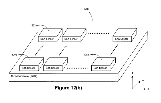
The nanosensors described above in connection with Figures 1-9 can be
combined to create an NxM array 1200 of multiple nanoscale EXX sensors 1202 as
shown in Figures 12(a) and 12(b). The values of N and M can be chosen by
practitioners of the present invention as a design choice based on their
intended use
of the nanoscale EXX sensors (e.g., 4x4, 16x16, 2x20, 64x64, etc. with upper
values
only bounded by manufacturing capabilities). For example, the inventors
contemplate that nanosensor matrix dimensions judging from current digital
display
technologies can also be 640x480, 800x600, 1024x768, 1600x1200, 2048x1536,
and 3200x2400. These nanoscale EXX sensors 1202 can be deposited on an array
substrate 1204 such as an SiO2 substrate. A preferred thickness for substrate
1204
is approximately 400 m, although other thicknesses can be used. It should be
noted that the voltage and current leads of the individual nanoscale EXX
sensors are
not shown in Figures 12(a) and (b) for ease of illustration. It should also be
noted
that a via design for row/column pin-out addressing from the matrix of
nanosensors
1202 in the array 1200 can be used, particularly for arrays having large
numbers of
nanosensors (see Figure 13). For the array structures shown in Figure 13, each
of
the 4-leads for the EXX sensors 1202 can be individually addressable, thereby
yielding 4n' pin-outs for an n x n array. Furthermore, these leads can be
selectively
combined to yield a reduction to 3n+ 1 pin-outs for an n x n array.
CA 02659674 2009-01-30
WO 2008/115258 PCT/US2007/074864
23
It should also be noted that in instances where the individual EXX sensors
are designed to have a substrate 106 of the same material as substrate 1204,
then
the EXX sensor 1202 that is located on array 1200 will not need to include
substrate
106 as the material of substrate 1204 can then serve as the appropriate
substrate.
However, if the substrate materials are dissimilar, then the individual EXX
sensors
1202 will preferably include their own substrate 106 (e.g., when the EXX
sensor
1202 has a GaAs substrate 106 while the array 1200 has an Si02 substrate
1204).
Preferably, the array 1200 exhibits tight spacing between EXX sensors 1202.
For
example, a spacing value that falls within a range of approximately 50 nm to
approximately 1000 nm can be used.
The selection of EXX sensor type(s) and distribution of EXX sensor type(s)
over the array 1200 can be highly variable. For example, the array 1200 can
include
only nanoscale EXX sensors 1202 of a single type (e.g., an array of only EAC
sensors,
an array of only EOC sensors, an array of only EEC sensors, etc.) Also, the
array
1200 can include a plurality of different types of nanoscale EXX sensors, such
as any
combination of nanoscale EMR/EPC/EAC/EOC/EEC sensors 1202. Integrating
multiple different types of EXX nanosensors in an array (such as EAC/EOC/EEC
nanosensors) will provide for a screening system capable of performing HCS for
prospective interrogation of cells based on the outcome of charge and
fluorescent
imaging, like LSC. However, the resolution of the acoustic subsystem will be
equal
to or greater than that obtained from optical microscopy, and moreover will
represent volumetric data (i.e., not be limited to a single focal plane at a
time), as the
time axis of the digitized ultrasound waveforms contains information that can
be
mapped to distance into the cell being imaged via the dispersion relationship
directly
analogous to imaging organ structures with currently available clinical
ultrasound
systems. This type of instrumentation would offer several advantages not
available
in current cytometry/microscopy instruments such as simultaneous acquisition
of
volumetric data based on nanoscale acoustic microscopy, higher resolution than
current optical microscopy without necessarily requiring expensive high
intensity
light sources, high precision and resolution surface charge measurements
without
the complications and ambiguities inherent in electrophoretic techniques, and
high
resolution, low noise fluorescent imaging.
It should also be noted that the array 1200 can be thought of as being
subdivided into a plurality of pixels 1400, as shown in Figure 14(a). Each
pixel 1400
CA 02659674 2009-01-30
WO 2008/115258 PCT/US2007/074864
24
can comprise one or more nanosensors 1202. For example, as shown in Figure
14(b), a pixel 1400 can comprise a plurality of different types of nanosensors
1202,
such as 4 nanosensors of types "A", "B", "C", and "D" (wherein type "A" could
correspond to an EOC nanosensor, wherein type "B" could correspond to an EPC
nanosensor, wherein type "C" could correspond to an EEC nanosensor, and
wherein
type "D" could correspond to an EMR nanosensor). Such groups of different
types of
nanosensors within a pixel 1400 can be helpful for increasing the sensitivity
of the
array 1200 by using signal averaging techniques on the voltage responses of
the
nanosensors.
Similarly, it should be noted that pixels 1400 or portions thereof can be
grouped with other pixels 1400 or portions thereof to form composite pixels.
For
example, Figure 15(a) depicts a composite pixel 1500 formed from a grouping of
4
pixels 1400 of the arrangement shown in Figure 14(b). Furthermore, the
composite
pixel 1500 can be formed of only a single type of nanosensors (e.g. only the
"A" type
nanosensors within those four pixels 1400, as shown by the boldface notation
in
Figure 15(a)). Once again, such arrangements of composite pixels can be
helpful for
increasing sensitivity through the use of signal averaging techniques.
Figure 15(b) depicts an example of a composite pixel 1502 that is formed
from a plurality of nanosensors of the same type that are arranged in a
straight line
and has a length of a plurality of pixels 1400 (e.g., the "A" type nanosensors
shown
in boldface within composite pixel 1502). Figure 15(b) also depicts an example
of a
composite pixel 1504 that is formed from a plurality of nanosensors of the
same
type that are arranged in a straight line orthogonal to composite pixel 1502
and has
a length of a plurality of pixels 1400. Composite pixels arranged such as
composite
pixels 1502 and 1504 can be useful for phase-type imaging of optical signals,
polarizing deflected light, or detecting different acoustical modes (e.g.,
shear,
transverse, various plate modes) depending on the type of nanosensor employed.
As an object such as one or more cells is placed into contact with the array
1200 on the exposed surfaces of the EXX sensors 1202, and as the EXX sensors
1202 of the array are perturbed, the voltage responses of the various EXX
sensors
1202 can be measured, digitized, stored, and processed by receiver electronics
including a signal processor (not shown). The collection of voltage responses
can in
turn be selectively pixelized based on the spatial relationship among the EXX
sensors to generate an image of the object that is indicative of one or more
CA 02659674 2009-01-30
WO 2008/115258 PCT/US2007/074864
characteristics of the object. Both single-modality images and multi-modal
parameterized images can be generated by registering and combining the output
from different types of nanosensors. Because of the nanoscale of the array's
EXX
sensors, the resultant images would also exhibit a resolution that is
nanoscale.
5 Furthermore, each nanoscale EXX sensor 1202 can be independently addressable
by
the receiver electronics to permit an increased data acquisition rate (imaging
frames
of a given area of an object per unit time). Also, it should be noted that to
enhance
the ability of cells to grow and adhere to the array surface, the exposed
surface of the
array on which the one or more cells contact the array can be coated with a
protein
10 such as fibronectin, vitronectin, collagen, or a protein-mimetic such as
poly-l-lysine
or silane.
For example, with an array 1200 comprised of multiple EAC and EEC
sensors 1202, after a cell is placed on that array, the array can be perturbed
with an
acoustic wave to obtain voltage responses from the EAC sensors from which an
15 ultrasonic image of the cell having nanoscale resolution can be generated.
At the
same time, the EEC sensors on the array 1202 can be perturbed with a surface
charge from the cell itself to produce voltage responses from the EEC sensors
from
which an image having nanoscale resolution and representative of the spatial
distribution of electric charge over the cell can be generated. Further,
still, because
20 the surface charge from the cell is not likely to perturb the EAC sensors
and because
the acoustic wave is not likely to perturb the EEC sensors, cross-talk between
the
EEC and EAC sensors can be minimized, and images of multiple characteristics
of
the cell can be simultaneously generated.
However, it should be noted that in instances where the array 1200 includes
25 both EAC/EPC sensors and EOC sensors, cross-talk can occur where the light
perturbation causes an undesired voltage response in the EAC sensor and the
acoustic perturbation causes an undesired voltage response in the EOC sensor.
To
reduce the effects of such cross-talk, one can selectively perturb the EAC
sensors at a
different time than the EOC sensors with sequentially applied perturbations
and
selective interrogation of the nanosensors based on which perturbation has
been
applied. In instances where the cell itself is the source of the light
perturbation
(presumably not a spontaneous light emission by the cell but rather a light
emission
following exposure to an external optical field), cross-talk can be reduced
when there
is a phosphorescent component present within the cell. In such a case, signal
CA 02659674 2009-01-30
WO 2008/115258 PCT/US2007/074864
26
processing techniques (lock-in amp, digital lock-in, pulse gating, time
correlation,
etc.) can be used to distinguish EAC and EOC signals. For EOC in the cases of
absorption and reflectance the response of the cell will be essentially
instantaneous,
e.g. the absorption and reflection signals will have essentially the same
profile as the
incident light signal with essentially no phase delay on the time scales of
relevance
here. So temporal separation of either absorption or reflection EOC from EPC
should not be problematic. In the case of fluorescence, the EOC signal will
depend
on the fluoroescence lifetime of the cell. If this is in the sub microsecond
range or
shorter, the fluorescence signal can be handled in the same way as absorption
and
transmission EOC. If it is of order a millisecond or longer, then an
(essentially DC)
EOC baseline shift can be added to the EPC signal but the signal above the
base line
should still be easily discernable. The corrollary is applicable for detection
of an
EPC signal in the presence of a long lived fluorescence, but by gating the
detection
system to coincide with the shorter time acoustic signal the baseline shift
can be
rejected. There are also hardware methods to accomplish signal selection. By
fabricating a substrate with thick and thin regions and depositing the EOC
sensors
on the thick regions and the EPC sensors on thin ones, the EOC regions can be
made impervious to acoustic signals, whatever their temporal properties.
Similarly,
by depositing a thin but optically opaque surface film on only the EPC
sensors, they
can be made impervious to any optical signals regardless of their temporal
properties.
The source of the pertubation(s) for the EXX sensors 1202 can be one or
more external perturbation sources as explained above, the object itself
(particularly
for EOC and EEC nanosensors), or a perturbation source that is integral to the
array.
For example, a laser source such as a near-field scanning optical microscope
(NSOM)
can use SAFT techniques to spatially localize a photon field to a small size
(on the
order of 1 micron or less and less than the spacing between EXX sensors on the
array) that can be scanned/driven in X and Y directions across the array by
the
piezoelectric X and Y motion controls of a scanning tunneling microscope (STM)
to
which the NSOM has been attached/adapted. The STM could be used to perturb
any EAC nanosensors while the NSOM could be used to perturb any EOC
nanosensors. The NSOM would guide light from the appropriate laser through a
submicron-sized aperture at the end of a tapered and metallized optical fiber.
The
near field method can provide photon fields with a lateral localization as
small as
CA 02659674 2009-01-30
WO 2008/115258 PCT/US2007/074864
27
500 nm in the visible region. Further still, a spatially localized field for
perturbing
EEC nanosensors could be obtained by mounting a tapered metallic tip to the
STM
scanner and applying a known voltage between the tip and a metallized back
surface
on the substrate 1204. For both the laser perturbation and the electric field
perturbation, the spatial resolution of the applied field would depend on its
maintaining close proximity to the surface of the sensor array. Such proximity
can
be maintained by feedback control of the STM's Z-motion via a signal from the
STM (guiding) tip.
It is also worth noting each of the array's EXX sensors can receive its own
biasing current flow such that not all of the array's EXX sensors will receive
the
same current flow. For example, EXX sensors 1-10 of an array may receive
current
A while EXX sensors 11-20 of that array may receive current B. As a further
example, 20 different currents could also be delivered to the array's 20 EXX
sensors.
Figures 16(a) and (b) illustrate another array embodiment for the present
invention wherein a perturbation source is integral to the array 1600. The
array
1600 includes an integral PZT transducer 1604 that serves to generate the
acoustic
wave for perturbing the array's EAC/EPC nanosensors 1202. As with the array
1200, the voltage and current leads of the individual nanoscale EXX sensors
1202
are not shown in Figures 16(a) and (b) for ease of illustration. However, it
should be
noted that ground-signal-ground (GSG) wiring geometries for electrical traces
deposited on substrate 1204 to the nanosensor leads can be employed to improve
characteristics in the UHF and SHF ranges of signal frequencies. With array
1600,
the EXX sensors 1202 and substrate 1204 can be arranged as explained above in
connection with Figures 12(a) and (b). However, due to the presence of the PZT
transducer 1604, it is preferred that at least some of the nanoscale EXX
sensors
1202 are EPC/EAC sensors. The array 1600 also preferably includes a transducer
backing material 1608 that lies in a plane substantially parallel to the plane
of
substrate 1204. A material and thickness for the backing material 1608 is
preferably
selected to have an acoustic impedance that is similarly-matched to the
acoustic
impedance of the piezoelectric thin-film transducer 1604 and lossy enough (to
attenuate the acoustic wave launched into the backing material) to minimize
undesired multiple reverberation resonance effects and to "spoil the Q" of the
thin-
film 1604 to effectively broaden the useful frequency bandwidth of the device
(corresponding to shorter time pulses and greater axial resolution). An
example of a
CA 02659674 2009-01-30
WO 2008/115258 PCT/US2007/074864
28
backing material 1608 could be an epoxy-resin with ground Tungsten particles.
However, it should be noted that other backing materials may be used as
explained
above. Furthermore, as the broadband transducer gets into the GHz range
(rather
than the MHz range), the inventors herein believe that the choice of backing
materials 1608 may be less impactful on performance.
Disposed between the substrate 1204 and the backing material 1608 is a
macroscale piezoelectric transducer 1604 in contact with a ground conductor
1602
and a hot conductor 1606. The macroscale piezoelectric transducer 1604 also
preferably lies in a plane that is substantially parallel to the plane of the
substrate
1204. By driving the piezoelectric transducer 1604 with a current flow through
conductors 1602 and 1606, the piezoelectric transducer emits a broadband
acoustic
plane wave whose plane is substantially parallel to the plane of substrate
1204 and
whose direction of propagation is substantially normal to the plane of
substrate
1204 (and by derivation in plane with the plane of the semiconductor/metal
interfaces 108 of the EPC/EAC nanosensors of the array). This broadband
acoustic
plane wave serves as the perturbation for the EPC/EAC nanosensors. The
piezoelectric transducer 1604 can be formed from a thin-film piezoelectric
transducer material, such as thin-film poly-crystalline or single crystal of
perovskite
ceramic materials (e.g., PZT: Lead Zirconate Titanate, and doped-derivatives
such as
PNZT: Niobium-doped PZT, PLZT: Lanthanum-doped PZT, PMN-ZT: magnesium
niobate-doped PZT, etc.), or polymer materials (e.g., PVDF: Polyvinylidene
difluoride) and exhibit a thickness between approximately 20 nm and
approximately
2000 nm to tune the frequency response to a desired range. However, it should
be
noted that other materials and thicknesses can be used. The frequency of the
broadband acoustic plane wave can be in the GHz range (e.g., approximately 1-5
GHz), although other frequency values can be used.
The broadband plane wave produced by the macroscale PZT transducer 1604
serves to improve the quality of images reconstructed from backscattered
ultrasound,
and the array 1600 permits insonification of an object being imaged at
pressure
levels that would be difficult to obtain using a nanoscaled acoustic
transmitter.
Moreover, by separating the transmit and receive elements (transducer 1604 and
nanosensors 1202 respectively), the receiving electronics (not shown) can be
greatly
simplified to permit higher drive levels on transmit and to improve both SNR
and
bandwidth aspects of signal receipt. Furthermore, by integrating both the
transmit
CA 02659674 2009-01-30
WO 2008/115258 PCT/US2007/074864
29
and receive elements into a single array, the need for external acoustic
perturbation
sources such as expensive SAMs can be avoided.
The integrated array 1600 or the array 1200 can be mass produced to provide
inexpensive (even disposable) imaging devices that could be incorporated into
the
bottoms of cell culture dishes 1700 (see Figure 17), thereby providing the
ability to
acoustically image either large numbers of or single cells and to continuously
provide
data that facilitates monitoring of the safety and efficacy of therapeutic
agents
intended for treatment of diseases such as cancer, heart disease, inflammatory
conditions, etc.
Figure 18 illustrates another embodiment of an imaging array in accordance
with the present invention. Figure 18 depicts a multi-element pitch-catch
array
1800. The array 1800 comprises 64 pairs of rectangular piezoelectric (e.g.,
PZT or
other piezoelectric materials such as described above) elements 1810 that are
spaced
evenly in a linear configuration of opposing pairs 1802 that are 20 m apart.
Base
1806 and supports 1804 hold the pairs 1802 of PZT elements 1810 in opposition
to
each other. Driving electronics (not shown) for delivering power to the PZT
elements will also be included in the array 1800. Exemplary dimensions for the
piezoelectric elements are 6.0 m high, 300 nm thick, 250 mn wide, and with a
50
nm spacing between elements (for a 300 nm element pitch and an overall azimuth
of 19.2 m for all 64 elements). However, other dimensions can be used,
wherein
Sol Gel deposition can be used as a technique to fabricate nanoscale PZT
elements.
The 64 PZT elements 1810 (that are shown in a front view in the bottom
portion of Figure 18) are configured to generate ultrasonic pulses that will
propagate
across the 20 m gap to their opposing partners, which will function as
receivers. In
a pulse/echo mode, the 64 PZT elements on the opposing side of the array will
act as
reflectors. An object to be imaged by array 1800 can be placed between the
opposing
pairs 1802 and ultrasound pulses can be used to generate ultrasound data from
which ultrasound images of the object can be reconstructed.
Furthermore, an NxM (e.g., 16x16) array like the one shown in Figures 12(a)
and (b) can be made of these PZT elements 1810, fabricated on the nanoscale,
for
use in the generation of ultrasound images. As with the arrays 1200 and 1600,
such
an array can be used to generate ultra high resolution images of a cancer cell
that is
grown on the array surface. Acoustic images of such a cancer cell can be made
with
ultrasound at frequencies such as 2.7 GHz or 5.2 GHz using SAFT techniques. To
CA 02659674 2009-01-30
WO 2008/115258 PCT/US2007/074864
improve such an array's SNR, the pulse-repetition frequency of the ultrasound
pulses may be increased, and/or signal averaging techniques can be used.
Because
the transmit frequency for the preferred ultrasound pulses is high (preferably
in the
GHz range; thereby implying short pulse lengths) and because the round trip
5 distance would be short, the inventors herein envision that signal averaging
for such
arrays will not face the usual problems that limit signal averaging's utility
to
conventional ultrasonics. It should also be noted that the arrays 1200 and
1600
described above could incorporate nanoscale PZT elements 1810 in combination
with the individual EXX sensors 1202 described above.
10 Figure 19 depicts a methodology for fabricating nanoscale EXX sensors using
a multi-step electron beam (e-beam) lithography process At step 1900, a thin
film
wafer of semiconductor material 102/902 is provided. Next at step 1902, a 30
nm
thick insulating film of Si3N4 (added to prevent shorting between the leads
and the
shunt) is deposited on the thin film wafer as a cap layer. At step 1904,
macroscopic
15 Au strips for wire bonding are deposited on the cap layer in a pattern that
radiates
outward from the edges of an 80 m square area that is defined on the
substrate
106/906. Next, at step 1906, a 30 nm thick calixarene film is spin coated onto
the
surface of the thin film wafer. At step 1908, four 30 nm x 3 m Au strips will
be
delineated in the calixarene in the corners of the 80 m square area by e-beam
20 lithography. This calixarene pattern and the macroscopic Au strips will
serve as a
mark for reactive ion etching (RIE) of the Si3N4 layer using conventional
methods
(step 1910). This RIE process (step 1910) produces a raised mesa of the thin
film on
its supporting substrate. For InSb films, an appropriate etchant is a CH4 + H2
mixture. The residual Si3N4 and Au strips serve as an RIE mask. Then, at step
25 1912, Au leads and an Au shunt will be deposited using a Ge stencil mask
and a
shadow evaporation technique. The inventors believe that such fabrication will
result in EXX nanosensors with a volumetric resolution of 35 nm (the voltage
probe
spacing set by the limits of suspended mask e-beam lithography) x 30 nm (the
width
of the mesa set by RIE etching properties and the resolution of calixarene
resist
30 patterns) x 25-250 nm (the thickness of the thin film material, along the x-
, y-, and
z-axes respectively. See Solin et al., Room temperature extraordinary
magnetoresistance of non-magnetic narrow-gap semiconductor/metal composites:
Application to read-head sensors for ultra high density magnetic recording,
IEEE
Trans Mag., 2002;38, pp. 89-94; Pashkin et al., Room-temperature Al single-
CA 02659674 2009-01-30
WO 2008/115258 PCT/US2007/074864
31
electron transistor made by electron-beam lithography, Applied Physics
Letters,
2000; 76, p. 2256; M. Sugawara, Plasma Etching, New York; Oxford, 1998, the
entire disclosures of each of which are incorporated by reference herein. As
would be
understood by a person having ordinary skill in the art, this technique can be
applied
to the fabrication of not only EPC, EAC, EOC, EMR, and EOC nanosensors but
also
EEC nanosensors (although the fabrication of the EEC nanosensors may be less
demanding because of the architectural difference therebetween).
To minimize leakage current through the floor of the mesa, an insulating
A1z,03 barrier can be first prepared by depositing and subsequently oxidizing
a layer
of Al to within 50 nm of the mesa sidewall. An alignment accuracy of about +/-
10
nm normal to the mesa sidewall is desired.
Furthermore, when fabricating an array 1200 or 1000, it is preferred that the
EXX nanosensors 1202 be designed and fabricated together as an array rather
than
individually fabricating each EXX nanosensor 1202 and then aggregating the
individual EXX nanosensors 1202 into an array.
Also, when fabricating an array of nanoscale EXX sensors, a substrate 1204
thinning process can be used to optimize the array's performance, although
this
thinning is preferably achieved using a feedback-controlled process that thins
the
substrate at increasingly slower and controllable rates to avoid a punch
through of
the EXX sensors through the substrate. Further still, when fabricating such
arrays of
interdigitated nanosensors, several additional mask steps can be used in the
suspended mask e-beam lithography process.
The SAFTs referenced above can be implemented using conventional SAFTs or
several variants thereof, wherein the variants of the conventional SAFT
algorithm
reduce the number of array elements required and offer improvements in SNR.
These variants include multielement-subaperture SAFT (see Gammelmark et al.,
"Multielement synthetic transmit apertum imaging using temporal encoding",
IEEE
Transactions on Medical Imaging, 2003; 22, pp. 552-63, the entire disclosure
of
which is incorporated herein by reference), which has been shown to achieve
higher
electronic signal to noise ratio and better contrast resolution than the
conventional
synthetic aperture focusing techniques. Another SAFT approach is based on
sparse
array SAFT which offers the advantage of a reduction in the number of array
elements (obtained at the price of lower transmitted and received signal).
These
drawbacks can be minimized by increasing the power delivered to each transmit
CA 02659674 2009-01-30
WO 2008/115258 PCT/US2007/074864
32
element and by using multiple transmit elements for each transmit pulse.
Another
SAFT option is to use a combination of B-mode and SAFT that has been shown to
improve lateral resolution beyond the focus of the transducer and by using
apodization to lower the sidelobes, but only at the expense of lateral
resolution, as
with classical synthetic aperture imaging. Results obtained by this technique
show
that, for a 15 MHz focused transducer, the 6-dB beamwidths at 3, 5, and 7 mm
beyond the focus are 189 m, 184 m, and 215 m, respectively. For images made
by scanning a 0.12 mm wire, SNR is 38,6 dB when the wire is at the focus, and
it is
32.8 dB, 35.3 dB and 38.1 dB after synthetic aperture processing when the wire
is 3,
5, and 7 mm beyond the focus, respectively. At 1-2 GHz, these beamwidths and
SNRs imply resolution would scale down to the nanometer range.
Figure 20 shows an approach to synthetic aperture imaging that follows
Frazier's description. Figure 20 depicts an array of elements labeled by the
index i.
In order to simplify the description, only the receive side of the imaging
problem
where each element is fired simultaneously will be considered. It is desired
to
process the backscattered signals S;(t) measured at each array element so that
those
signals are effectively focused at the point P. This may be achieved by
appropriately
delaying various signals from the array elements and summing them ("delay-and-
sum" beam forming). The field from the array will be focused at the point P if
all
pulses from the array elements arrive there simultaneously. This can be
effected in
post-processing if one shifts each backscattered pulse by
Ot; =2z/c(1- 1+ idlz )
and then summing each of the received waveforms according to:
A(t) N', (P)S1(t - Ot; )
where the w;(P) terms are weights assigned to each element and are functions
of the
chosen focal point P and also array element transmit properties that affect
the field
it transmits. These weights are used to achieve aperture apodization, which is
necessary to obtain increased resolution. The inventors have obtained
satisfactory
results using a unit rectangle function whose width is determined by the
transducer
used to acquire raw data. See Bracewell, RN, The Fourier Transform and its
Applications, New York, McGraw-Hill, 1978, the entire disclosure of which is
incorporated by reference herein. For applications where higher resolution is
desired
CA 02659674 2009-01-30
WO 2008/115258 PCT/US2007/074864
33
such as with the nanosensors described herein, other apodizations such those
described by Frazier can be used.
While the present invention has been described above in relation to its
preferred embodiment, various modifications may be made thereto that still
fall
within the invention's scope. Such modifications to the invention will be
recognizable upon review of the teachings herein. For example, the nanosensor
embodiments described herein have been described as having a generally
rectangular
plate shape. It should be noted that other geometries could be used for the
nanosensors. For example, a circular semiconductor material with an embedded
concentric metallic shunt. Also, it should be noted that the inventors
envision that
the nanoscale EXX sensors and/or arrays of such nanoscale EXX sensors can be
implanted into a patient's body (such as within a patient's vasculature) for
imaging
internal bodily conditions of the patient. These sensors or arrays could be
implanted in much that same way that subcutaneous pumps, or cardiac pacemakers
and defibrillators, or the routes for any prosthetic device are implanted. The
inventors contemplate that delivery and deployment via intravascular catheters
would be used. Such nanosensors and arrays can be configured with a telemetric
output, such as by transmitters incorporated into the arrays that produce
signals
(e.g. radio signals) that can be monitored remotely with appropriate
receivers, as it
the case with implanted pacemakers, to provide in vivo ultra high resolution
imaging of internal body conditions and processes or they can include on-board
local
memory in which the voltage responses can be stored for subsequent analysis
upon
retrieval of the array. For biasing currents, the nanosensors or arrays can be
configured with their own on board energy sources.
Further still, the nanosensors and arrays of the present invention may also be
used for other non-medical applications, including but not limited to real-
time in-
process monitoring of any nanoscale events detectable by the sensors and
incorporation into field sensors for environmental monitoring. For example,
the
inventors envision that nanoscale EOC sensors can be useful as position
sensitive
detectors and as photosensors and that nanoscale EEC sensors can be useful for
pixel monitoring in flat panel displays.
Accordingly, the full scope of the present invention is to be defined solely
by
the appended claims and their legal equivalents.