Note: Descriptions are shown in the official language in which they were submitted.
CA 02659706 2000-03-27
WO 00/60475 PCT/SG00/00045
1
A SYSTEM FOR MONITORING CONNECTION
PATTERN OF DATA PORTS
FIELD OF THE INVENTION
The present invention relates to the field of cabled systems and related
computer peripheral devices, and more particularly to a system and method for
determining interconnection pattem of data ports without n:quifing special
patching cables or patching panels.
BACKGROUND OF THE INVENTION
The problems of tradcing the interconnection pattem among the various
ports in a local area network are well known to those skilled in the arL At
least
one system which deals with this problem is described in the US Patent No.
5,483,467 entitled "Patching Panel Scanner". The patent describes a patching
panel scanner which automaticaity and continuously senses the interconnection
anangement of various ports such as computer ports and user ports. In this
type of system, the interconnection between the ports are provided b y
patching cables or a{tematively by apparatus of intemal connecfion in patching
panels such- as the CLPP cordless patching panel available from RIT
Technologies Ltd. of Tel Aviv, Israel.
In this type of system, in order to determine the interconnectiviiy pattem
of the various ports, a conductor needs to interconnect the ports and deliver
a
signal to the scanner indicating the connection status of a parbcxalar port.
In the
modem computer era, it is actually difficult to provide a conductor for this
purpose because most modem data cables being used to interconnect various
CA 02659706 2000-03-27
WO 00/60475 PCT/SG00/00045
2
devices have to meet a particular pre-determined standard in the industry. So
for instance, a standard cable such as RJ45 eight wires per cable, each having
an end which is adapted to mate with an RJ45 port. No free wire allows for
scanning for interconnectMty.
Therefore, in the prior art scanner systems, the ports needed to b e
interconnected via a patch panel which required a special patch cable or an
apparatus of intemal connecdons in the patch panels. In any case, the ports
could not be connected directly using standard cables. Although the need for
and desirability of having a scanner system which can utilize standard cables
cleariy exist, so far, the industry has been unable to come up with such a
system.
OBJECT OF THE INVENTION
It is therefore an objective of the present invention to provide a system
for monitoring and determining the interconnectivity of ports which overcomes
the shortcomings of the prior art system described above.
More particulatiy, it is an object of present invention to provide a system
for monitoring and determining the interconnectivdy of ports which does not
require special patch panels or patch cables.
More particularly, it is an object of present invention to provide a system
for monitoring and determining the interconnectivity of ports which utilizes
standard connection cables.
SUMMARY OF THE INVENTION
CA 02659706 2000-03-27
= t WO 00/60475 PCT/SGOO/00045
3
The present invention determines and monitors the connection pattem of
data ports which are connected by multiconductor cables without requiring
special patch cables or patch panels. In order to electronically determine the
connectivity between one port to another, it is generally well understood that
an
electrical conductor needs to connect one port to the other. Although this
principle is well known, in the modem era where many of the standardized
cables such as RJ1 1 and RJ45 are used, it is d'ifficuft to provide this
dedicated
conductor for connect'nrity-scanning purposes because each of the wires within
the cable is used for a standardized purpose which may interfere with the
1.0 connectivity-scanning operation.
In the present connectivity monitoring system, a dedicated conductor
which may be attached to an existing cable is provided. The conductor
interacts with an adapter board which is attached to a port where the cable is
to
be connected. To provide an additional contact point for the scanning
operation, an adapter jacket is provided which attaches to an RJ45 jadc. The
adapter jacket is attached to the jack at both ends of the cable. The
additional
contact point for the scanning operation is provided via an extemal contact
located on the outside of the adapter jacket. An extemal conductor wire
connects the extemal contact of the jack at each end of the cable such that
the
contact at each respective end will be electrically coupled to each other.
To provide a contact point for the extemal contact of the adapter jacket at
the port site, an adapter board is provided above the port sockets with each
of
the sockets having a socket contact. The socket oontact is positioned such
that
when the RJ45 jack having the adapter jacket is inserted into a socket, the
conW of the adapter jacket electrically mates with the socket contact of the
adapter board.
CA 02659706 2000-03-27
= ; :
WO 00/60475 PCT/SGOO/00045
4
In the overall system, the adapter board is coupled to an output module
and an input module. The output driver module has a plurality of output
drivers,
and the receiver module has a plurality of latches (other similar electronic
devices can be used instead of latches). Each of the socket contacts is
uniquely connected to one output driver and one latch. The output module and
the input module are both coupled to a m'icro-processor which is in tum
coupled
to a communication interfaoe. The system may be coupled to a local area
network or to a computer to report the information regarding the connection
pattem.
Both the output module and the input module can be implemented
using standard IC devices. The main function of the output module is to
provide a plurality of output drivers which address the adapter contacts and
to
send a signal to the contacts when instructed to do so by the micro-processor.
The main funcaon of the input module is to provide a plurality of latches (or
other similar devices) which also address the contacts and to receive the
signal
sent by the output drivers. The corrxnmication interface can also b e
implemented using standard devices cumendy available to interface between
the micro-processor and local area network and electronic devices.
Now to describe the operation of the present system, the micro-
processor has pre-designated one output driver as a first driver and the
socket
contact which it is connected to as the first contact. The latch in the input
module
which is connected to the designated first contact is designated as the first
latch.
The port corresponding to the first socket contact is considered to be the
first
port. Another driver is pre-designated as a second driver, and it.s
corresponding socket contact is designated as a second contact and itss
corresponding latch is designated as a second iatch. The same designation
. . . . . . . . . . . . . . . .
CA 02659706 2000-03-27
WO 00/60475 PCT/SGOO/00045
scheme is applied to third, fourth, fifth, and so on, driver/contact/latch
groupings
such that all groups are uniquely designated.
Initially, all of the socket contacts are at low state with no signal being
sent
to them by the output module. To monitor the connectivity of the various
ports,
5 the micro-processor causes the designated first output driver to send out a
pulse signal to the socket contact which the micro-processor has designated as
the first contact. This places the first socket contact at a high state, and
consequently, also places the first latch in the input module at the high
state.
After sending out the signal, the micro-processor scans the input module for a
latch having a high state. If only the first latch andicates a high, then the
rrdcro-
processor concludes that no valid connection has been made between the first
port and another port. If, however, a port other than the first port, port
one,
indicates a high state, for instance port seven, then the micro-processor
concludes that the port is validly connected to port seven. Once the
connectivity state of port one is determined, the resuft is stored in memory
and
the same process is repeated for port two and so on until all of the ports'
connection status has been determined.
BRIEF DESCRIPTION OF THE DRAWINGS
FIG. 1 A is a perspective illustration of a currat RJ45 cable which can
be adapted to work with the present system.
FIG. 1 B is a perspective illustration of the RJ45 cable of FIG. 1 A which
has been fitted with an adapter jacket of the present invention.
FIG. 1 C is an isolated perspective llustration of an adapter jacket of the
present invention which is adapted for an RJ45 cable jack.
CA 02659706 2000-03-27
WO 00/60475 PCT/SGOO/00045
6
FIG. 2 is a front view of a plurality of RJ45 sockets fitted with an adapter
board of the present invention.
FIG. 3 is a simplified schematic illustration of the present connectivity
monitoring system.
FIG. 4 is a simplified schematic iliustration which shows the relationship
between the output drivers, the socket contacts, and the receiver latches.
FIGS. 5A, 5B, 5C Olustrate various other standard cables which can be
adapted for use with the present system.
FIGS. 6A, 6B, 6C illustrate various other standard cables which can b e
adapted for use with the present system.
FIGS. 7A, 7B, 7C illustrate various other standard cables which can be
adapted for use with the present system.
FIG. 8 is a simplified schematic Blustration of the present connectivity
monitoring system incorporating the optional diagnostic pen.
FIG. 9 is a simplified schematic llustration which shows the relationship
between the output drivers, the socket oontacts, the receiver latches, and the
pen input latch.
FIG. 10 illustrates an embodiment where the extemal contact is a pin
which is supported by a spring.
FIG. 11 illustrates an embodiment where the exterrmal contact is placed in
the jack itself.
FIG. 12 illustrates adapter strip which is fabricated out of flex tape.
FIG. 13 is a simplified schematic lfustration of the present connectivity
monitoring system incorporating the optional diagnostic pen and LCD units.
FIG. 14 is a simplified schematic illustration which shows the relationship
between the output drivers, the socket contacts, the receiver latches, the pen
input latch, and LCD drivers.
CA 02659706 2000-03-27
WO 00/60475 PCT/SG00/00045
7
DETAILED DESCRIPTION OF THE INVENTION
In order to electronically determine the connectivity between one port to
another, it is generally well understood that an electrical conductor needs to
connect one port to the other. Although this principle is well known, n the
modem era where many of the standardized multi-conductor cables such as
RJ11 and RJ45 are used, ft is difficult to provide this dedicated conductor
for
connectivity-scanning purposes because each of the wires within the cable is
used for a standardized purpose which may interfere with the connectivity-
scanning operation. Although it may be possible to share an existing wire n
the cable for the scanning operation, this would require additional cir+cxuiby
for
differentiating between the signals used for the scanning purposes and the
signals used for other purposes such as data transfer. Moreover, in many
cases, it may be impossible to effectively share an existing wire or
conductor.
In the present connectivity monitoring system, a dedicated conductor
which may be attached to an existing cable is provided. The conductor
interacts with an adapter board which is attached to a port where the cable is
to
be connected. Ahhough in descdbing the preferred embodiment of the
present invention, a specific cablelport combination utilizing a common
standard
such as RJ45 will be shown, it should be appreciated that this is done for
illustration purposes only, and is not meant to limit the present invention to
this
illustrative example.
Now in referring to FIG. 1a, a standard RJ45 cable 3 having a jadc 5 is
shown. Although only one end of the cable is shown here in FIG. la for
illustration purposes, it should be understood that a similar jack is attached
to the
other end of the cable. The RJ45 jack 5 has eight standard contact points 6.
CA 02659706 2000-03-27
WO 00/60475 PCT/SGOO/00045
8
To provide an additional contact point for the scanning operation, an adapter
jacket 7, FIG. 1 c, is provided which attaches to the RJ45 jadc as shown in
FIG.
1 b. The adapter jacket is attached to the jadc 5 at both ends of the cable 3
(though only one is shown in the figure). The additional contact point for the
scanning operation is provided via an extemal contact 8 located on the outside
of the adapter jadcet 7. An external conductor wire 9 connects the extemal
contact 8 of the jack 5 at each end of the cable 3 such that the contact 8 at
each
respective end will be electrically coupled to each other.
Now referring to FIG. 2, a plurality of RJ45 sockets is shown which are
standard sockets which mate with a standard RJ45 jadc. The sockets may be
ports for a network equipment such as a 10 Base-T hub, PABX, and key-
phone system, or may be part of a patch panel, though a special patch panel
is not required for a successful operation of the present system. To provide a
contact point for the extemal contact 8 of the adapter jacket 7, an adapter
board
14 is provided above the sockets 12 with each of the sockets 12 having a
socket oontact 15. The socket contact 15 is positioned such that when the
RJ45 jack 5 having the adapter jacket 7, as shown in FIG. 1 B, is inserted
into a
socket 12 of FIG. 2, the contact 8 of the adapter jadcet 7 electrically mates
with
the socket contact 15 of the adapter board 14. Afthough here the adapter
board 14 is shown to cany a plurality of socket contacts 15, it is entirely
possible, and sometimes desirable, to have an adapter board 14 which canies
only one socket contact which is used on a single isolated socket
Referring now to FIG. 3, a simplified schematic iilustralon of the present
system 1 is shown. The adapter board 14 of FIG. 2 is coupled to an output
module 18 and input module 19. As shown in more detail in FIG. 4, the output
driver module 18 has a pl.uraliiy of output drivers 20, and the n3ceiver
module
19 has a plurality of latches 25 (other similar electronic devices can be used
CA 02659706 2000-03-27
WO 00/60475 PCT/SG00/00045
9
instead of latches). Each of the socket contacts 15 is uniquely connected to
one
output driver 20 and one latch 25. The output module 18 and the input module
19 are both coupled to a micro-processor 21 which is ai tum coupled to a
communication interface 22. The system 1 may be coupled to a local area
network 23 or to a computer 24 to report the infomiation regarding
connectivity.
Both the output module and input module can be implemented using
standard IC devices. The main function of the output module 18 is to provide a
plurality of output drivers 20 which address adapter contacts 15 and to send a
signal to the contacts 15 when instructed to do so by the micro-processor 21.
The main function of the input module 19 is to provide a plurality of latches
25
(or other similar devices) which also address the contacts 15 and to receive
the
signal sent by the output drivers. The communication interface 22 can also be
implemented using standard devices currently available to interface between
the micro-processor 21 and local area network 23 and electronic devices.
Now to describe the system 1 in greater detail, the adapter board 14
shown in FIG. 3 is placed over port sockets (not shown in FIG. 3 but shown in
FIG. 2). The micro-processor 21 has pre-designated one output driver as a
first driver and the socket contact which it is connected to as the first
contact. The
latch in the input module 19 which is conneded to the designated first oontact
is
designated as the first latch. The port corresponding to the first socket.
contaa
is considered to be the first port. Another driver is pre-designated as a
second
driver, and its corresponding socket oontact is designated as a second contact
and its corresponding latch is designated as a second latch. The same
designation scheme is applied to third, fourth, fifth, and so on,
driver/contact/latch groupings such that all groups are uniquely designated.
Of
course, the designations are somewhat arbitrary and the paraadar designation
. . . .. . . . . .. . .
CA 02659706 2000-03-27
WO 00/60475 PCT/SGOO/00045
number or scheme is not important so long as the individual groupings are
uniquely traceable by the micro-processor 21.
Initially, all of the socket contacts 15 are at low state with no signal being
sent to them by the output module 18. To monitor the connectiniity of the
5 various ports, the micro-processor 21 causes the designated first output
driver
to send out a pulse signal to the socket conW 15 which the micro-processor
21 has designated as the first oontact. This places the first socket contact
at a
high state, and consequently, also places the first latch in the input module
19 at
the high state. After sending out the signal, the micro-processor 21 scans the
10 input module 19 for a latch having a high state. If only the first latch
indicates a
high, then the micro-processor 21 concludes that no valid connection has been
made between the first port and another port. If, however, a port other than
the
first port, port one, indicates a high state, for instance port seven, then
the
micro-processor 21 concludes that the port 1 is validly connected to port
seven. Once the connectivity state of port one is determined, the result is
stored in memory and the same process is repeated for port two and so on
until all of the ports' connection status has been determined.
While other scanning scheme can be employed with the present
system, the scheme described above is the one employed in the -preferred
embodiment. The advantage of the scheme described above is that it allows
any port to be connected to any other port. This is unlike patch panel
scanning
systems where one panel may need to be designated as the input panel, and
the other panel is designated as the output panel, and a cable needs to
connect a port from the output panel to a port from the input panel. The cable
cannot connect, for instance, a port from the input panel to another port from
the
same input panel. This feature is particularly useful for the present
invention
CA 02659706 2000-03-27
WO 00/60475 PCT/SGOO/00045
11
because no special patch panels are required, and so the ports may b e
randomly spread out in no particular order.
In some situations, a user may wish to know the identity of a particular
data port which has been fitted with the present invention. In previous
systems, unless the port is properly labeled at the socket site, it is
difficult for a
user to ascertain the identity of the port without tracing the cable
cotunecdng the
port all the way to its source. To provide a solution to this problem, the
present
system can optionally include a diagnostic pen which can assist in identifying
a
port simply by making contact with the socket contact corresponding to the
port
the user wishes to identify.
The block diagram of the present system incorporating this diagnostic
pen is shown in FIG. 8. As shown in FIG. 8, the pen 80 has an electrica0y
conductive tip 82. The tip 82 is electrically coupled to a pen input module
84.
The pen input module 84 is communicably coupled to the micro-processor 21.
As shown in greater detail in FIG. 9, the pen input module 84 basically
comprise a single latch 27 (or other similar device) for receiving an
electrical
signal.
To determine which socket contact 15 is making contact with the tip 82 of
the diagnostic pen 80, the micro-processor 21 continually monitors the status
of
the pen input module 84. As explained above, the output module continually
sends out an electrieal signal to each of the socket contacts 15. Because each
of the socket contacts 15 is uniquely addressed at the output module 18, each
socket contact 15 is uniquely traceable. Therefore, the micro-processor 21 is
aiways able to uniquely determine which socket contact 15 is being sent the
electrical signal by the output module 18 at any given moment. Initially, when
the tip 82 of the pen 80 is not making oontact with any of the socket
contacts,
the pen input module 84 is at a low state because it has not receive any
. ... . . .. . . .
CA 02659706 2000-03-27
WO 00/60475 PCT/SG00/00045
12
electrical signal. When the tip 82 touches one of the socket contacts 15,
however, the pen input module 84 goes high. By determining which socket
contact 15 the output module 18 has sent the signal to when the pen input
module 84 goes high, the micro-processor 21 is able to determine which
socket contact 15 has made contact with the pen tip 82. The data port
corresponding to that particular socket contact 15 then can be identified.
To further assist in the identfioation of the data ports, and also to
facilitate
greater flexibility to the present system, the present system can optionally
further include liquid crystal display (LCD) urirts 100 for each of the ports
as
shown in FIG. 13. The LCD units 100 are mounted adjacent to the data ports,
and are communicably coupled to an LCD module 102. The detailed
schematic is shown in FIG. 14. The LCD module 102 basically comprise a
plurality of output drivers 28 which are uniquely connected to the LCD units
100. The LCD un'its 100 will indicate information about a particular port, or
a
row of ports. For instance, the LCD unit may indicate the device which is
connected to the port, the user name, IP address, etc. The LCD may be used
in oonjunction with the pen 80 such that by touching the socket contact of a
particular port, the micro-processor sends the information about the port to
the
LCD unit corresponding to the socket contact which made contact with the pen
80. The LCD units 100 may also cany an interactivve feature where a user can
select different options based on a simple menu such as a YES/NO menu
scheme where the. user can indicate his choice by touching the socket contact
(or altematively a separate dedicated contact pad for the LCD units) with the
pen 80. Although here the LCD units 100 were shown here to be separate
units, it should be understood that -a single oartinuous strip of LCD may be
used.
CA 02659706 2000-03-27
WO 00/60475 PCT/SGOO/00045
13
Although the present invention has been illustrated using the RJ45
standard, one skilled n the art should appreciate that the present invention
can
be implemented using other existing standards. Some such examples are
shown in FIG. 5, 6, and 7, where the cuffently available SC connectors, ST
connectors, and BNC connectors, respectively, are fitted with an adapter
jacket
and their respective ports are provided with an adapter board.
In FIG. 5, 5A, 5B, and 5C, a standard SC connector 30 is fitted with an
adapter jacket 31 having a contact 32 to yield an adapted SC connector 33.
Also, the SC connector sockets 35 have been fitted with adapter boards 34
with adapter contact points 36.
In FIG. 6, 6A, 6B, and 6C, a standard ST connector 40 is fitted with an
adapter jacket 41 having a contact 42 to yield an adapted ST connector 44.
Also, the ST connector sockets 45 have been fdted with adapter boards 44
with adapter contact points 46.
In FIG. 7, 7A, 7B, and 7C, a standard BNC connector 50 is fitted with an
adapter jacket 51 having a contact 52 to yield an adapted BNC connector 55.
Also, the BNC connector sockets 55 have been fitted with adapter boards 54
with adapter contact points 56.
In an aftematnre embodiment of the present invention, the external
contact 8 of the adapter jacket 7(as shown in FIG.1 c) is in the form of a
oontad
pin 60 as shown ki FIG. 10. In this embodiment, the pin 60 is slidably
engaged in a barrel 62 which is placed inside the adapter jacket 64. The
oontact pin 60 is supported by a spring 66 which resides inside the barrel 62
and provides tension to the pin 60 when it is depressed in the direction shown
by the arrow 65. The tension provided by the spring 66 .allows the contact pin
60 to make better contact with the socket contact 15 of the adapter board 14
(FIG. 2). It should be appreciated by those slalied 'n the art that although a
. . .. . . . . . . .
CA 02659706 2000-03-27
WO 00/60475 PCTISGOO/00045
14
spring was shown here, the spring 66 may be replaced with other devices that
can provide the necessary tension to the pin 60.
In another embodiment of the present invention, the extemal contact is
placed within the standardized jack itself. An example of such an embodiment
is shown in FIG. 11: Here, the contact pin 70 is placed on the RJ45 jack 72
itseff. Similar to the embodiment shown in FIG. 10, the contact pin 70 is
slidably engaged in a barrel 74 and also supported by a spring 76. It is to be
understood however, that it is possible to have an extemal contact without the
barrel 74 and the spring 76. In this embodiment, the socket contact is placed
inside the socket itself to make contact with the contact pin 70.
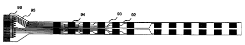
In yet another embodiment of the present invention, a flex tape may be
used to form an adapter strip 90, as shown in FfG.12, which is an embodiment
of the adapter board. The adapter strip 90 may be provided with an adhesive
such that it can be conveniently pasted adjacent to the sockets. The adapter
strip 90 comprises a main body 92 and a head poraon 93 which are fabricated
from flex tape which is a common substrate material currently being used to
support electronic circuitry. The main body 92 has a plurality of contacts 94
which are spaced in correspondence with the spacing of the data ports for
which the adapter strip is to be placed adjacent to. Two rows of contacts may
be provided such as shown in FIG. 12 to accommodate two rows of ports
located above and below the adapter strip 90. However, an adapter strip
having only a single row is clearly possible. Each contact 94 is connected by
a
conductor such as a wire which ends in a conductor strip 96 at the head
portion
93. The wire strips 96 provide a convenient way to eiectrically mate the
adapter strip 90 to the output 18 and input modules 19.
In yet another embodiment of the present invention, the socket contact
is in the form of a port or a socket which tightly mates with the extemal
contact.
CA 02659706 2000-03-27
WO 00/60475 PCT/SGOO/00045
In yet another embodiment of the present invention, the adapter jacket is
integrated with the standardized multi-conductor cable.
The present invention may be embodied in other specific forms without
departing from the spirit or essential characteristics thereof. The presently
5 disclosed embodiments are, therefore, to be considered in all respects as
illustrative and not restrictive, the scope of the invention being indicated
by the
appended claims and all changes which come within the meaning and range of
equivalency of the claims are, therefore, to be embraced therein.