Note: Descriptions are shown in the official language in which they were submitted.
CA 02660080 2009-02-05
WO 2008/019157 PCT/US2007/017734
THIN-FILM EAS AND RFID ANTENNAS
BACKGROUND
Field of the Disclosure
The present disclosure relates to antenna assemblies for electronic article
surveillance (EAS) or radiofrequency identification (RFID) which are made of
thin films
and/or thin film materials.
Background of Related Art
Electronic article surveillance (EAS) systems project a electromagnetic field
into an interrogation zone usually at the exit of a retail store. The
electromagnetic field
excites a marker that returns a signal to the EAS system which alarms to
indicate the
presence of,an EAS marker within the interrogation zone. EAS markers may be
placed on
merchandise to prevent unauthorized removal of tagged merchandise from a
retail
establishment, while EAS system transmitter antennas are used to project the
electromagnetic field into the interrogation zone. EAS system receiver
antennas are used
to detect the returned signal from the EAS masker. EAS system transceiver
antennas are
constructed to perform both transmit and receive functions. By proper design
and
configuration of the EAS antennas, the system may provide an electromagnetic
field of
sufficient intensity to adequately excite the EAS marker and provide adequate
receive
sensitivity so that the return signal received by the EAS system may be
detected above the
electromagnetic noise in the retail environment.
= Properly designed EAS system antennas provide electromagnetic fields that
provide the following characteristics:
= cover the entire interrogation.zone with sufficient intensity field to
excite
an EAS marker;
= have adequate intensity in all spatial orientations throughout the
interrogation zone;
= do not extend beyond the interrogation zone at high intensities that
would
cause tagged merchandise outside the interrogation zone to alarm the
system; and
= comply with regulatory requirements for electromagnetic field emissions.
CA 02660080 2009-02-05
WO 2008/019157 PCT/US2007/017734
In addition, because the interrogation zone is often located in locations
where
retailers desire to display merchandise for sale, typical EAS antenna systems
are either
concealed or small and streamlined so that the system installation meets the
retailer's
aesthetic requirements.
In addition, the system also needs to be designed so that the transmitter(s)
and
the antenna(s) meet the various regulatory or safety agency requirements.
Traditional EAS systems have relied on antennas that are placed in pedestals
positioned on opposite sides of an entrance. The antennas project the magnetic
field across
the opening. However, there is a practical limit as to how wide of an opening
may be
covered by an EAS system due to limitations in the size of the antennas and
the regulatory
or safety limitations on the intensity of the electromagnetic field strength.
As a result, the use of pedestals is often impractical to provide an
interrogation
zone to cover very large openings such as those at mall entrances or exits due
to the
challenges in meeting the above listed requirements.
In order to adequately cover a wide area such as a mall entrance or exit, an
array of several wire loop antennas may be buried in the concrete under the
flooring. Such
loop antennas are designed as transceivers and project magnetic fields into
the region
above the floor to detect the returned signal from the EAS marker. Typically
these types of
antennas are capable of covering an interrogation zone extending up to about
1.2 meters
above the floor. Such an antenna also has the advantage of being modular so
that it may be
extended to cover various width openings. One such system is marketed by
Sensorrnatic
Electronics (Boca Raton, Florida, USA) under the brand name "Floormax".
Typically, this type of design has the following installation characteristics:
= The antenna coils are mounted in the floor and require significant
excavation of the sub-floor for installation;
= After installation the antennas are encased in concrete that is re-poured
over
and around the antennas making them inaccessible without further
excavation.
In installations where no metal is present the antennas may be mounted over
the sub-floor without excavation. But, due to the thickness of the antenna
coil, when
antennas are mounted above the sub-floor, layers of additional concrete must
be floated
onto the surface of the sub-floor to form a gradual slope to cover the
antenna. This
2
CA 02660080 2014-05-23
77496-295
gradually sloped region may extend several feet on all sides of the antenna.
This concrete
work is often expensive and may be impractical in some cases.
U.S. Patent Application Publication No. US 2004/0135690 AI, entitled "WIDE
EXIT ELECTRONIC ARTICLE SURVEILLANCE ANTENNA SYSTEM" by Copeland.
et. al., published on July 15, 2004, and U.S. Patent Application Publication
No. US
2004/0217866 Al, also entitled "WIDE EXIT ELECTRONIC ARTICLE
SURVEILLANCE ANTENNA SYSTEM" by Copeland et al., published November 4,
2004, describe several different systems to cover wide exits or entrances and
use various
combinations of the following antenna characteristics:
= overhead / ceiling mounted ferrite core transceiver or transmitter
antennas;
= side / wall mounted ferrite core transceiver or transmitter antennas;
= overhead / ceiling mounted wire-loop transceiver or transmitter antennas;
= side/wall mounted wire-loop transceiver or transmitter antennas;
= perimeter wire-loop transceiver or transmitter antennas that extend around
the entire perimeter of the interrogation zone;
= side / wall mounted core receiver antennas;
= overhead / ceiling mounted core receiver antennas;
= floor mounted core receiver antennas designed to be mounted in trenches
in
the sub-floor;
= floor mounted loop receiver antennas also designed to be mounted in small
trenches in the sub-floor.
However, systems using receivers in the floor still require cutting trenches
in
the sub-floor for routing of wire-loop or core receiver antennas. This is
often undesirable
due to the expense and inconvenience to the retailer.
Other efforts have been disclosed using a perimeter wire-loop transceiver or
transmitter antenna with added overhead / ceiling mounted or side / wall
mounted core
receiver antennas to cover the interrogation zone. This solution has been
successfully
deployed for openings up to 3 meters high and about 5 meters in width. Again,
this
system also requires cutting trenches in the floor to install wire-loop
antenna which is
undesirable.
As a result, many known approaches require excavation or trenching of the
3
CA 02660080 2009-02-05
WO 2008/019157 PCT/US2007/017734
subfloor to allow installation.
SUMMARY OF THE INVENTION
The embodiments of the present disclosure provide a very thin antenna
structure that may be used as a transmitter antenna, a receiver or a
transceiver that is thin
enough to be mounted under the flooring without any need for cutting or
modification of
the structure of the subfloor.
More particularly, the present disclosure relates to an antenna assembly
particularly suitable for an electronic article surveillance (EAS) and/or a
radiofrequency
i 0 identification (RFID) network. In one embodiment, the antenna assembly
is capable of
being installed in a structure wherein the structure comprises a covering and
a substructure
and the antenna assembly is configured with thin film materials to have a
total thickness
such that the antenna assembly can be disposed between the substructure and
the covering.
The antenna assembly may have a total thickness not greater than about 15
millimeters
(mm).
The antenna assembly may include at least one of (a) a transmitter antenna (b)
a transceiver antenna, and (c) a receiver antenna, with the receiver antenna
being
configured as one of an air core antenna and a non-air core antenna. The
antenna
assembly may include a base insulating layer, and at least one of the
transmitter antenna,.
the transceiver antenna and the receiver antenna may be at least partially
disposed on the
base insulating layer. The base insulating layer may include a common planar
surface,
and at least one of the transmitter antenna, the transceiver antenna and the
receiver antenna
may be at least partially disposed on the common planar surface of the base
insulating
layer.
The receiver antenna may be configured as a non-air core receiver antenna and
may be substantially disposed in an internal compartment that is over the
common planar
surface of the base insulating layer or within the base insulating layer. The
antenna
assembly may further include an enclosure insulating layer. The enclosure
insulating layer
may be at least partially disposed on the at least one of the transmitter
antenna, the
transceiver antenna and the receiver antenna. The antenna assembly may further
include a
support insulating layer, with the base insulating layer being at least
partially disposed on
the support insulating layer. A filler insulating layer may be at least
partially disposed
between the base insulating layer and the support insulating layer.
4
CA 02660080 2009-02-05
WO 2008/019157 PCT/US2007/017734
In one embodiment, the transmitter antenna and/or the transceiver antenna
and/or the receiver antenna may include at least one antenna trace conductor
including a
start end conductor layer portion and a finish end conductor layer portion
each having a
thickness, wherein the finish end conductor layer portion crosses one of over
and under the
start end conductor layer portion to form an end crossover section of the
antenna
assembly, and wherein the end crossover section includes the antenna trace
conductor and
an antenna assembly base insulating layer having a thickness and disposed
between the
start end conductor layer portion and the finish end conductor layer portion.
In one embodiment, the antenna assembly may be at least partially housed
within a housing assembly, with the housing assembly configured with thin film
materials
such that both the housing assembly and the antenna assembly can be disposed
between
the substructure and the covering. The housing assembly may include the
enclosure
insulating layer, the base insulating layer and an outer wall along an outer
periphery of the
antenna assembly so that the housing assembly at least partially houses the
antenna
assembly thereby. The housing assembly may further include an inner wall along
an inner
periphery of the antenna assembly, so that the housing assembly at least
partially houses
the antenna assembly thereby. The housing assembly may be configured such that
the
antenna assembly is hermetically sealed. When the antenna assembly is at least
partially
housed within a housing assembly, the housing assembly may be configured with
thin film
materials such that both the housing assembly and the antenna assembly can be
disposed
between the substructure and the covering.
In one embodiment, when the receiver antenna is configured as a non-air core
receiver antenna and is substantially disposed in the internal compartment
within the base
insulating layer, the base insulating layer may have a thickness including a
first sub-layer
having a thickness, a second sub-layer having a thickness, and a base sub-
layer disposed
therebetween having a thickness wherein the base sub-layer includes the
internal
compartment defined therein formed by the first and second sub-layers. The
receiver
antenna configured as a non-air core receiver antenna may include a wire loop
at least
partially coiled around at least one bar of magnetic material formed in a thin-
film
construction.
5
CA 02660080 2014-05-23
77496-295
According to one aspect of the present invention, there is provided an
Electronic Article Surveillance ("EAS") antenna assembly for use in
conjunction with a
structure, the structure comprising a substructure and a covering, the EAS
antenna assembly
comprising: a substrate comprising a first portion and a second portion, the
substrate being a
base insulating layer; a first EAS transceiver antenna and a second EAS
transceiver antenna,
the first EAS transceiver antenna being disposed on the first portion of the
substrate, the
second EAS transceiver antenna being disposed on the second portion of the
substrate in a co-
planar orientation with respect to the first EAS transceiver antenna, the
second EAS
transceiver having one of an air core and a non-air core; and thin film
materials forming said
substrate, first EAS transceiver antenna and second EAS transceiver antenna
such that the
antenna assembly can be disposed between the substructure and the covering
without altering
a structural feature of the structure; an enclosure insulating layer at least
partially disposed on
at least one of the first and second EAS transceiver antenna; the antenna
assembly being at
least partially housed within a housing assembly, the housing assembly
configured with thin
film materials such that both the housing assembly and the antenna assembly
can be disposed
between the substructure and the covering.
According to another aspect of the present invention, there is provided an
Electronic Article Surveillance ("EAS") antenna assembly for use in
conjunction with a
structure, the structure comprising a substructure and a covering, the EAS
antenna assembly
comprising: a substrate comprising a first portion and a second portion, the
substrate being a
base insulating layer; a first EAS transceiver antenna and a second EAS
transceiver antenna,
the first EAS transceiver antenna being disposed on the first portion of the
substrate, the
second EAS transceiver antenna being disposed on the second portion of the
substrate in a co-
planar orientation with respect to the first EAS transceiver antenna, at least
one of the first and
second EAS transceiver antennas being disposed on a common planar surface of a
base
insulating layer, the second EAS transceiver being a non-air core transceiver
antenna
substantially disposed in an internal compartment of one of (a) over the
common planar
surface of the base insulating layer and (b) within the base insulating the
base insulating layer
having a thickness including: a first sub-layer having a thickness; a second
sub-layer having a
thickness; and a base sub-layer disposed therebetween having a thickness,
wherein the base
5a
CA 02660080 2014-05-23
77496-295
sub-layer includes the internal compartment defined therein formed by the
first and second
sub-layers; and thin film materials forming said substrate, first EAS
transceiver antenna and
second EAS transceiver antenna such that the antenna assembly can be disposed
between the
substructure and the covering without altering a structural feature of the
structure.
According to still another aspect of the present invention, there is provided
an
Electronic Article Surveillance (EAS) antenna assembly for use in conjunction
with a
structure, the structure comprising a substructure and a covering, the EAS
antenna assembly
comprising: a substrate comprising a first portion and a second portion; a
first EAS
transceiver antenna and a second EAS transceiver antenna and a receiver
antenna, the first
1 0 EAS transceiver antenna being disposed on the first portion of the
substrate, the second EAS
transceiver antenna being disposed on the second portion of the substrate in a
co-planar
orientation with respect to the first EAS transceiver antenna, the receiver
antenna configured
as a non-air core comprising a wire loop at least partially coiled around at
least one bar of
magnetic material formed in a thin-film construction; and thin film materials
forming said =
1 5 substrate, the first EAS transceiver antenna and second EAS transceiver
antenna such that the
antenna assembly can be disposed between the substructure and the covering
without altering
a structural feature of the structure.
5b
CA 02660080 2009-02-05
WO 2008/019157 PCT/US2007/017734
BRIEF DESCRIPTION OF THE DRAWINGS
The subject matter regarded as the embodiments is particularly pointed out and
distinctly claimed in the concluding portion of the specification. The
embodiments,
however, both as to organization and method of operation, together with
objects, features,
and advantages thereof, may best be understood by reference to the following
detailed
description when read with the accompanying drawings in which:
FIG. 1 is a plan view of a single loop air core transmitter or transceiver
assembly using thin film construction and partially illustrating a housing
assembly housing
the transmitter or transceiver assembly according to one embodiment of the
present
disclosure;
FIG. IA is a plan view of the area of detail of the transmitter or transceiver
assembly and partially illustrated housing assembly of FIG. 1;
FIG. 1B is a cross-sectional elevation view of the area of detail of the
transmitter or transceiver assembly and housing assembly completely
illustrated at a cross-
5 over region taken along line 1B-1B of FIG. 1 A and as disposed in a
floor;
FIG. 1B' is a cross-sectional elevation view of the area of detail of the
transmitter or transceiver assembly at a cross-over region and a variation of
the completely
illustrated housing assembly taken along line 1B'-1B' of FIG. IA and as
disposed in a
floor;
FIG. 1C is a cross-sectional elevation view of the completely illustrated
housing assembly and transmitter or transceiver assembly taken along line 1C-
1C of FIG.
1 and as disposed in a floor;
FIG. 1C' is a cross-sectional elevation view of the variation of the
completely
illustrated housing assembly and transmitter or transceiver assembly taken
along line 1C'-
1C' of FIG. 1 and as disposed in a floor;
FIG. 2 is a plan view of an alternate embodiment of a single air core
transmitter
or transceiver loop winding antenna assembly using thin film construction
methods and
partially illustrating a housing assembly housing the antenna assembly
according to the
present disclosure;
FIG. 2A is a plan view of the area of detail of the single transmitter or
transceiver loop assembly and partially illustrated housing assembly of FIG.
2;
FIG. 2B is a cross-sectional elevation view of the area of detail of the
transmitter or transceiver assembly and the housing assembly completely
illustrated at a
6
CA 02660080 2009-02-05
WO 2008/019157 PCT/US2007/017734
cross-over region taken along section line 2B-2B of FIG. 2 and as disposed in
a floor;
FIG. 2B' is a cross-sectional elevation view of the area of detail of the
transmitter or transceiver assembly at a cross-over region and a variation of
the completely
illustrated housing assembly taken along line 2B'-2B' of FIG. 2 and as
disposed in a floor;
FIG. 2C is a cross-sectional elevation view of the completely illustrated
housing assembly and transmitter or transceiver assembly taken along line 2C-
2C of FIG.
2 and as disposed in a floor;
FIG. 2C' is a cross-sectional elevation view of the transmitter or transceiver
assembly and the variation of the completely illustrated housing assembly
taken along line
2C'-2C' of FIG. 2;
FIG. 3 illustrates one embodiment of an antenna assembly showing separate air
core transmitter and receiver windings using thin film construction and
partially
illustrating a housing assembly housing the antenna assembly according to the
present
disclosure;
FIG. 3A is a plan view of the area of detail of the antenna assembly showing
separate transmitter and receiver windings and of the partially illustrated
housing assembly
of FIG. 3;
FIG. 3B is a cross-sectional elevation view of the area of detail of an end
cross-
over region of the housing assembly completely illustrated and antenna
assembly of FIGS.
3 and 3A taken along section line 3B-3B of FIG. 3A and as disposed in a floor;
FIG. 3B' is a cross-sectional elevation view of the area of detail of an end
cross-over region of the housing assembly completely illustrated and antenna
assembly of
FIGS. 3 and 3A taken along section line 3B-3B of FIG. 3A and as disposed in a
floor;
FIG. 3C is a cross-sectional elevation view of the area of detail of an end
cross-
over region of the antenna assembly and housing assembly completely
illustrated of FIGS.
3 and 3A taken along section line 3C-3C of FIG. 3A and as disposed in a floor;
FIG. 3C' is a cross-sectional elevation view of an end cross-over region of
the
antenna assembly and housing assembly completely illustrated of FIGS. 3 and 3A
taken
along section line 3C-3C of FIG. 3A and as disposed in a floor;
FIG. 3D is a cross-sectional elevation view of the completely illustrated
housing assembly and antenna assembly taken along line 3D-3D of FIG. 3 and as
disposed
in a floor;
FIG. 3D' is a cross-sectional elevation view of the antenna assembly and the
7
CA 02660080 2009-02-05
WO 2008/019157 PCT/US2007/017734
variation of the completely illustrated housing assembly taken along line 3D'-
3D' of FIG.
3
FIG. 4 is a plan view illustrating one embodiment of an air core antenna
assembly showing a single transmitter winding with multiple receiver windings
and
partially illustrating a housing assembly housing the antenna assembly
according to the
present disclosure;
FIG. 4A is a cross-sectional elevation view of the antenna assembly and
housing assembly completely illustrated taken along section line 4A-4A of FIG.
4 and
disposed in a floor;
FIG. 5 is a plan view illustrating one embodiment of an air core antenna
assembly with multiple transmitter and multiple receiver windings and
partially
illustrating a housing assembly housing the antenna assembly according to the
present
disclosure;
FIG. 5A is a cross-sectional elevation view of the antenna assembly and
housing assembly completely illustrated taken along section line 5A-5A of FIG.
5 and
disposed in a floor;
FIG. 6 is a plan view illustrating one embodiment of an air core antenna
assembly with multiple transceiver windings and partially illustrating a
housing assembly
housing the antenna assembly according to the present disclosure;
FIG. 6A is a cross-sectional elevation view of the antenna assembly and
housing assembly completely illustrated taken along section line 6A-6A of FIG.
6 and
disposed in a floor;
FIG. 7 is a plan view illustrating thin film conductors for an alternative
antenna
assembly having a transmitter antenna assembly with an internal compartment
for a non-
air core receiver antenna assembly and partially illustrating a housing
assembly according
to the present disclosure;
FIG. 7A is a cross-sectional elevation view of the antenna assembly of FIG. 7
with the housing assembly completely illustrated and taken along line 7A-7A of
FIG. 7
and as disposed in a floor;
FIG. 7B is a cross-sectional elevation view of the antenna assembly of FIG. 7
and a variation of the completely illustrated housing assembly taken along
line 7B-7B of
FIG. 7 and as disposed in a floor;
8
CA 02660080 2009-02-05
WO 2008/019157 PCT/US2007/017734
FIG. 7C is a cross-sectional elevation view of the antenna assembly of FIG. 7
and an alternate embodiment of the completely illustrated housing assembly
taken along
line 7C-7C of FIG. 7 and as disposed in a floor;
FIG. 7D is an enlarged view of a portion of the antenna assembly and housing
assembly shown in FIG. 7C;
FIG. 7E is an enlarged view of another portion of the antenna assembly and
housing assembly shown in FIG. 7C;
FIG. 8 is a plan view illustrating thin film conductors for an alternative
antenna
assembly having a pair of transmitter antenna assemblies each with an internal
compartment for a non-air core receiver antenna assembly and partially
illustrating a
housing assembly according to the present disclosure; and
FIG. 8A is a cross-sectional elevation view of the antenna assembly of FIG. 8
with the housing assembly completely illustrated and taken along line 8A-8A of
FIG. 8
and as disposed in a floor;
9
CA 02660080 2009-02-05
WO 2008/019157 PCT/US2007/017734
DETAILED DESCRIPTION
Numerous specific details may be set forth herein to provide a thorough
understanding of the embodiments of the invention. It will be understood by
those skilled
in the art, however, that various embodiments of the invention may be
practiced without
these specific details. In other instances, well-known methods, procedures,
components
and circuits have not been described in detail so as not to obscure the
various
embodiments of the invention. It can be appreciated that the specific
structural and
functional details disclosed herein are representative and do not necessarily
limit the scope
of the invention.
It is worthy to note that any reference in the specification to "one
embodiment"
or "an embodiment" according to the present disclosure means that a particular
feature,
structure, or characteristic described in connection with the embodiment is
included in at
least one embodiment. The appearances of the phrase "in one embodiment" in
various
places in the specification are not necessarily all referring to the same
embodiment.
Some embodiments may be described using the expression "coupled" and
"connected" along with their derivatives. For example, some embodiments may be
described using the term "connected" to indicate that two or more elements are
in direct
physical or electrical contact with each other. In another example, some
embodiments
may be described using the term "coupled" to indicate that two or more
elements are in
direct physical or electrical contact. The term "coupled," however, may also
mean that
two or more elements are not in direct contact with each other, but yet still
co-operate or
interact with each other. The embodiments are not limited in this context.
The present disclosure relates to a very thin antenna structure that may be
used
as a transmitter, a receiver or a transceiver that is thin enough to be
mounted under the
flooring without any need for cutting or modification of the structure of the
subfloor.
Various embodiments of the antenna assembly are shown that provide for single
or
multiple transmitter or transceiver loop antennas; single or multiple receiver
loop
antennas; and separate transmitter and receiver loop antennas.
Turning now to the specific embodiments of the present disclosure, FIGS. 1,
1A, 1B and 1C illustrate an embodiment of a single loop transmitter or
transceiver
assembly using thin film construction that may be used for EAS or RFID systems
according to the present disclosure. More particularly, FIG. 1 is a plan view
of single loop
transmitter or transceiver assembly 100a using thin film construction. For
purposes of
CA 02660080 2009-02-05
WO 2008/019157 PCT/US2007/017734
simplification, FIG. 1 only partially illustrates a housing assembly 1100
housing the
transmitter or transceiver assembly 100. FIG. lA is a plan view of the area of
detail of the
transmitter or transceiver assembly 100a and partially illustrated housing
assembly 1100
of FIG. 1. FIG. 1B is a cross-sectional elevation view of the area of detail
of the
transmitter or transceiver assembly 100a and housing assembly 1100 completely
illustrated at a cross-over region taken along line 1B-1B of FIG. 1A. FIG. 1C
is a cross-
sectional elevation view of the completely illustrated housing assembly 1100
and
transmitter or transceiver assembly 100a taken along line 1C-1C of FIG. 1. As
described
in more detail below, the housing assembly 1100 includes an outer wall 1110
and an inner
wall 1120.
Antenna assembly 100a includes an antenna 101 at least partially disposed on a
common planar surface 165 of antenna assembly base substrate or insulating
layer 160.
Antenna 101 includes an antenna trace conductor 102 having a start end
conductor layer
portion 104 and a finish end conductor layer portion 106. The antenna trace
conductor
102 may be configured as a rectangular spiral as illustrated in FIGS. 1 and
1A. However,
alternate configurations such as square, circular, elliptical, or other such
shapes may be
employed. The embodiments are
not limited in this context. The start end conductor layer portion 104 forms
one end of the
rectangular spiral while the finish end conductor layer portion 106 forms
another end of
the rectangular spiral.
As shown in FIG. 1, starting at a first corner region 108 with the start end
conductor layer portion 104, the antenna trace conductor 102 proceeds in an
inward spiral
to second, third and fourth corner regions 110, 112 and 114, respectively, to
form a first
loop 116. At the first corner region 108, the antenna trace conductor 102
proceeds to form
a second loop 118, parallel to first loop 116, in an inward spiral to second,
third and fourth
comer regions 110, 112 and 114, respectively. Similarly, at the first corner
region 108, the
antenna trace conductor 102 proceeds to form a third loop 120, parallel to
first loop 116
and second loop 118, in an inward spiral to second, third and fourth corner
regions 110,
112 and 114, respectively. Those skilled in the art will recognize that a
greater or a fewer
number of loops 116 to 120 may be employed to configure the antenna 101, and
that three
loops 116, 118 and 120 are by way of illustration only. Therefore, the antenna
101 is
configured to have a multiplicity of loops such as loops 116 to 120. The
embodiments are
not limited in this context.
11
CA 02660080 2009-02-05
WO 2008/019157 PCT/US2007/017734
Although the loops 116, 118 and 120 are described as spiraling inwardly, the
loops 116, 118 and 120 may be described as, or installed on the antenna
assembly base
insulating layer 160 in a manner so as to effect, an outward spiral as opposed
to an inward
spiral. The embodiments are not limited in this context.
As best shown in FIGS. 1A and 1B, at the first corner region 108, the third
loop
120 terminates at a winding trace termination122 substantially transverse to
the first,
second and third parallel loops 116, 118 and 120. At termination position 122,
the
antenna trace portion 102 interfaces with the finish end conductor layer
portion 106. The
finish end conductor layer portion 106, via a cross-over member 124, crosses
either over
to or under the start end conductor layer portion 104 to form an end cross-
over region 126 at
the first comer 108. In one embodiment, the cross-over member 124 is in
electrical
communication with the antenna trace conductor 102 through a via connection
128
disposed in proximity to the winding trace termination 122. The cross-over
member 124
extends either under, as shown in FIGS. 1, IA and 1B, or over (not shown) the
first,
second and third parallel loops 116, 118 and 120 to a finish connection 130.
The cross-
over member 124 is in electrical communication with the finish connection 130
through a
via connection 132. As a result, the finish connection 130 is in electrical
communication
with the antenna trace conductor 102 through the via connections 128 and 132
and the
cross-over member 124. In one embodiment, the finish connection 130 is
disposed
substantially parallel to and adjacent the first loop 116 such that the finish
end conductor
layer portion 106 forms an L-shape.
As best illustrated in FIG. 1B, the end crossover region 126 includes the
antenna trace conductor 102 and the base insulating layer 160 disposed between
the start
end conductor layer portion 104 and associated loops 116, 118 and 120 and the
finish end
conductor layer portions 106, and, in particular, the cross-over member 124.
Therefore,
the start end conductor layer portion 104 and the finish end conductor layer
portion 106
are electrically isolated from each other. The end crossover region 126 of the
antenna
assembly 100a may also be configured to be disposed on an antenna assembly
support
insulating layer 150. More particularly, the crossover member 124 is disposed
on the
support insulating layer 150. In one embodiment, as specifically illustrated
in FIG. 1B, a
dummy or filler insulation or insulating layer 155 may be disposed adjacent to
the
crossover member 124 and between the insulating layer 160 and the support
insulating
layer 150.
12
CA 02660080 2009-02-05
WO 2008/019157 PCT/US2007/017734
The antenna assembly 100a may also include an antenna assembly enclosure or
top cover insulating layer 170 at least partially disposed over the antenna
assembly 100a
and over the common planar surface 165. In addition, the antenna assembly 100a
is
configured such that the end cross-over region 126, the antenna trace
conductor 102, the
support insulating layer 150, the base insulating layer 160, and the enclosure
insulating
layer 170 are each constructed of a thin film made from a thin film material.
In particular,
the electrically conductive members which are included in the end cross-over
region 126,
such as the antenna trace termination 122, the cross-over members 124, the
finish
connection 130, and the antenna trace conductor 102, may be constructed of a
thin film of
conductive printing, copper tape, or other suitable electrically conductive
material capable
of being applied in a thin film layer. The thin film material of the
electrically insulating
members such as first, second and third insulating layers 150, 160 and 170 may
be
selected from the group consisting of polyvinylidene fluoride (PVDF), sold
under the trade
name Kynar by Elf Atochem North America, Inc. of Philadelphia, Pennsylvania,
USA or
Solef by Solvay America, Inc. of Houston, Texas, USA, or a polyester film,
sold under
the trade name Mylar by E.I. du Pont de Nemours and Company, Wilmington,
Delaware, USA, either of which is capable of being applied in a thin film
layer. The
foregoing materials are specified by way or example only and those skilled in
the art will
recognize that other suitable materials may be employed.
As a result of construction using the thin film material, a total maximum
height
H1 is defined by the thickness of the cross-over member 124, the base
insulating layer 160
over the cross-over member 124, and the first, second and third parallel loops
116, 118
and 120 and the finish connection 130 over the base insulating layer 160. The
total
maximum height H1 ranges up to 0.7 millimeters (mm).
In one embodiment, when the antenna assembly 100a further includes the
support or bottom insulating layer 150 and the enclosure insulating layer or
top cover 170,
a total maximum height H1' is defined by the thickness of the support or
bottom insulating
layer 150, the cross-over member 124 over the support insulating layer 150,
the base
insulating layer 160 over the cross-over member 124, the first, second and
third parallel
loops 116, 118 and 120 and the finish connection 130 over the base insulating
layer 160,
and the enclosure insulating layer or top cover 170 over the first, second and
third parallel
loops 116, 118 and 120 and the finish connection 130.
As illustrated in FIG. 1B, a structure such as a floor 5 of an edifice or
13
CA 02660080 2009-02-05
WO 2008/019157 PCT/US2007/017734
establishment (not explicitly shown) includes a substructure or subfloor 10
and a covering
such as a flooring or floor covering 20. Those skilled in the art will
recognize that and
understand how the structure may also be a wall or ceiling or other portion,
either indoors
or outdoors, of the edifice or establishment. Similarly, the substructure may
be a wall
interior, ceiling interior or the like. The covering may be a wall board or
ceiling surface or
the like. The embodiments are not limited in this context. However, for the
purposes of
illustration throughout the present disclosure, the structure is referred to
as floor 5 of an
edifice or establishment, the substructure is referred to as subfloor 10, and
the covering is
referred to as flooring or floor covering 20.
The antenna assembly 100a is configured with the thin film materials, which
include the electrically conductive end cross-over region 126, such as the
antenna trace
termination 122, the cross-over members 124, the finish connection 130, and
the antenna
trace conductor 102, and the electrically insulating layers 150, 160 and 170,
to have a
total thickness, as represented by the total maximum height H1', such that the
antenna
5 assembly 100a may be disposed between the subfloor 10 and the flooring or
floor covering
20, without significantly altering the structural features of the floor or
causing a
deleterious effect to pedestrians or pedestrian traffic on the floor. The
total maximum
height H1' ranges up to about 15 mm, although in most applications, the total
maximum
height Hr ranges up to about 1.3 mm. Length L1 and width W1 of the antenna
assembly
100a may be in the range of about 65 cm by about 155 cm, respectively,
although the
embodiments are not limited in this context.
In one embodiment, the antenna assembly 100a may be configured such that
when the support insulating layer 150 and/or the enclosure insulating layer or
top cover
170 is omitted, the total maximum height H1 equals the total maximum height
H1' when
the support insulating layer 150 and/or enclosure insulating layer or top
cover 170 are
included. More particularly, the support or bottom insulating layer 150 may be
omitted
when the subfloor 10 itself provides an adequate electrically insulating
effect. However,
to protect the antenna assembly 100a from environmental conditions such as
moisture
fluctuations, the antenna assembly 100a may be housed at least partially, if
not entirely,
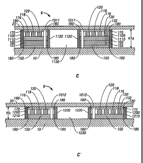
within the housing assembly 1100. As illustrated in FIGS. 1, 1B and 1C, base
insulating
layer 160 may be at least partially disposed on the support insulating layer
150. A dummy
or filler insulation or insulating layer 155 may be at least partially
disposed between the
base insulating layer 160 and the support insulating layer 150. The housing
assembly
14
CA 02660080 2009-02-05
WO 2008/019157 PCT/US2007/017734
1100 includes an outer wall 1110 extending around an outer periphery 1115 of
the antenna
assembly 100. The outer wall is joined to the enclosure insulating layer 170
and may be
joined to the base insulating layer 160 to at least partially enclose and
house the antenna
assembly 100a. The housing assembly 1100 may include an inner wall 1120
extending
around an inner periphery 1125 of the antenna assembly 100. The inner wall
1120
encloses a region 1130 which may be empty space or may contain holes for
permeation of
tile adhesive as explained below. The inner periphery 1125 and portions
adjacent thereto
may be formed of a solid material.
In one embodiment, as illustrated in FIGS. 1B and 1C, the housing assembly
1100 may include by incorporation the support insulating layer 150 as a lower
lid and
enclosure insulating layer 170 as an upper lid of the housing assembly 1100.
The outer
and inner walls 1110 and 1120, respectively, may be joined at least partially,
if not
entirely, to the support insulating layer 150 and to the enclosure insulating
layer 170 at
joints 180 to form a hermetic seal. The housing assembly 1100 further includes
a series of
mounting sleeves or rings 1011 that are positioned as required in the portions
of the
housing assembly 1100 adjacent to the inner periphery 1125. Six mounting
sleeves or
rings 1011 by way of example are illustrated in FIG. 1, one each in the
vicinity of the four
corners formed by the region 1130 and the inner periphery 1125 of the of the
inner walls
1120, and one each midway in the lengthwise direction of housing assembly 1100
on
either side of the inner periphery 1125.
With the flooring 5 removed, the sub-floor 10 is cleaned. The housing
assembly 1100 containing the antenna assembly 100a is laid out on the sub-
floor 10 at the
location desired. Anchor holes (not shown) are drilled in the sub-floor 10 to
accommodate
mounting screws (not shown) corresponding to the series of mounting sleeves or
rings
1011. Once the housing assembly 1100 is mounted in the desired location using
the
mounting screws, a tile adhesive may be placed in the open region 1130 which
may be
empty space or may contain holes for permeation of the tile adhesive.
Referring now to FIGS. 1, 1A, 1B' and 1C', in a variation of the embodiment of
the housing assembly 1100, an antenna assembly 100b may be incorporated into a
housing
assembly 1200. The housing assembly 1200 and antenna assembly 100b are
identical to
housing assembly 1100 and antenna assembly 100a, respectively, except that, as
illustrated
in FIG. 1B', at the cross-over region 126, the support insulating layer 150'
on which the
cross-over member 124 is disposed and merges by the upward bend 151 with the
base
CA 02660080 2009-02-05
WO 2008/019157 PCT/US2007/017734
insulating layer 160 to form the corner region or joint 156. The dummy or
filler insulation
155 is now omitted throughout the antenna assembly 100' except for the cross-
over region
126.
Referring also to FIG. 1C', the housing assembly 1200 now includes an outer
wall 1210 extending around an outer periphery 1215 of the antenna assembly
100'. The
housing assembly 1200 may include an inner wall 1220 extending around an inner
periphery 1225 of the antenna assembly 100'. The outer and inner walls 1210
and 1220,
respectively, may be joined at joints 180 to the enclosure insulating layer
170 and to the
base insulating layer 150 to at least partially enclose and house the antenna
assembly 100b
thereby. The inner wall 1220 now encloses a region 1230 which may be empty
space or
may contain holes for permeation of tile adhesive as previously explained
above. The
inner periphery 1225 and portions adjacent thereto may be formed of a solid
material. In a
manner analogous to mounting sleeves or rings 1011 of housing assembly 1100,
the
housing assembly 1200 further includes a series of mounting sleeves or rings
1012 that are
positioned as required in the portions of the housing assembly 1200 adjacent
to the inner
periphery 1225.
By comparing the housing assembly 1100 and antenna assembly 100a
illustrated in FIG. 1C to the housing assembly 1200 and antenna assembly 100b
illustrated
in FIG. 1C, it is evident that for the same thicknesses of the materials being
incorporated,
height Hla of the outer wall 1110 and inner wall 1120 of housing assembly 1100
is
greater than height Hlb of the outer wall 1210 and inner wall 1220 of housing
assembly
1200. Therefore, the housing assembly 1200 provides a lower profile, except at
the
crossover region 126, as compared to the housing assembly 1100.
FIGS. 2, 2A, 2B and 2C illustrate an alternate embodiment of a single loop
transmitter or transceiver assembly for EAS or RFID using thin film
construction
according to the present disclosure. More particularly, FIG. 2 illustrates an
alternate
embodiment of the single transmitter or transceiver loop winding antenna
assembly 100a
or 100b using thin film construction methods. Again, for purposes of
simplification, FIG.
2 only partially illustrates a housing assembly 1100' housing air core antenna
assembly
100a' or 100b'. FIG. 2A is a plan view of the area of detail of the single
transmitter or
transceiver loop assembly 100a' or 100b' and partially illustrated housing
assembly of
FIG. 2. FIG. 2B is a cross-sectional elevation view of the area of detail of
the transmitter
or transceiver assembly 100a and the housing assembly 1100' completely
illustrated at a
16
CA 02660080 2009-02-05
WO 2008/019157 PCT/US2007/017734
cross-over region taken along section line 2B-2B of FIG. 2. FIG. 2C is a cross-
sectional
elevation view of the completely illustrated housing assembly 1100' and
transmitter or
transceiver assembly 100a' taken along line 2C-2C of FIG. 2. Again, as
described in more
detail below, the housing assembly 1100' includes an outer wall 1110' and
inner wall
1120.
More particularly, antenna assembly 100a' includes an antenna 101' at least
partially disposed on the common planar surface 165 of substrate or base
insulating layer
160. Antenna 101' includes the antenna trace conductor 102 having start end
conductor
layer portion 104 and a finish end conductor layer portion 106'.
Antenna 101' is identical to antenna 101, the difference being that the finish
end conductor layer portion 106' in first corner 108 has an L-shaped
combination cross-
over member and finish connection 134 which is in electrical communication
with the
antenna trace 102 through the via connection 128 which is disposed in
proximity to the
winding trace termination 122. The L-shape of the combination cross-over
member and
finish connection 134 is formed by a first branch 136 and a second branch 138
disposed
transversely to one another to form an L-shape.
As best shown in FIGS. 2A and 2B, the combination cross-over member and
finish connection 134 crosses either under, or over (not shown), the start end
conductor
layer portion 104 to form an end cross-over region 126' at the first corner
108. More
particularly, the first branch 136 crosses under the third loop 120 and the
second loop 118
and only a portion of the first loop 116. The second branch 138 is partially
disposed under
the start end conductor layer portion 104 such that a lateral edge 140 of the
second branch
138 extends past a lateral edge 142 of the first loop 116. The antenna 101' is
configured
to have a multiplicity of loops such as loops 116 to 120.
The end crossover region 126' includes the antenna trace conductor 102 and the
base insulating layer 160 disposed between the start end conductor layer
portion 104 and
associated loops 116, 118 and 120 and the finish end conductor layer portion
106', and, in
particular, the combination cross-over member and finish connection 134.
Therefore, the
start end conductor layer portion 104 and the finish end conductor layer
portion 106' are
electrically isolated from each other.
Those skilled in the art will recognize that, and understand how, in that the
antenna assembly 100 as previously discussed with respect to FIGS. 1, lA and
1B, and the
antenna assembly 100' are operated by alternating current, the designation of
end
17
CA 02660080 2009-02-05
WO 2008/019157 PCT/US2007/017734
conductor layer portion 104 as the start end conductor layer portion and the
designation of
end conductor layer portion 106 and end conductor layer portion 106' as the
finish end
conductor layer portion are chosen arbitrarily for convenience of description
only and that
end conductor layer portion 104 may also be described as the finish end
conductor layer
portion and end conductor layer portion 106 and 106' may also be described as
the start
end conductor layer portion.
As illustrated in FIG. 2B, the antenna assembly 100' may also include the top
cover or enclosure insulating layer 170. In addition, the antenna assembly
100' is
configured such that the electrically conductive members included in the end
cross-over
region 126', and the antenna trace conductor 102, and the electrically
insulating members
such as substrate or support insulating layer 150, the base insulating layer
160, and the top
cover or enclosure insulating layer 170 are each constructed of a thin film
made from a
thin film material, as discussed previously. The end cross-over region 126'
may be formed
of the same materials as previously described for end cross-over region 126.
As a result of construction using the thin film material, a total maximum
height
H2 is defined by the thickness of the combination cross-over member and finish
connection 134, the base insulating layer 160 over the combination cross-over
member
and finish connection 134, and the first, second and third parallel loops 116,
118 and 120
over the base insulating layer 160. The total maximum height H2 ranges up to
about 0.7
mm.
In one embodiment, when the electrode assembly 100' further includes the
support or bottom insulating layer 150 and the enclosure insulating layer or
top cover 170,
a total maximum height H2' is defined by the thickness of the support or
bottom insulating
layer 150, the combination cross-over member and finish connection 134 over
the support
insulating layer 150, the base insulating layer 160 over the combination cross-
over
member and finish connection 134, the first, second and third parallel loops
116, 118 and
120 over the base insulating layer 160, and the enclosure insulating layer or
top cover 170
over the first, second and third parallel loops 116, 118 and 120. The total
maximum
height H2' ranges up to about 1.3 mm although dimensions as large as about 15
mm are
possible.
In one embodiment, the antenna assembly 100' may be configured such that
when the support or bottom insulating layer 150 and/or the enclosure
insulating layer or
top cover 170 are/is omitted, the total maximum height H2 equals the total
maximum
18
CA 02660080 2009-02-05
WO 2008/019157 PCT/US2007/017734
height 112' when the support or bottom insulating layer 150 and/or the
enclosure insulating
layer or top cover 170 are/is included.
Again, to protect the antenna assembly 100a' from environmental conditions
such as moisture fluctuations, the antenna assembly 100a' may be housed at
least partially,
if not entirely, within the housing assembly 1100'. As illustrated in FIGS. 2,
2B and 2C,
base insulating layer 160 may be at least partially disposed on the support
insulating layer
150. The dummy or filler insulation or insulating layer 155 may be at least
partially
disposed between the base insulating layer 160 and the support insulating
layer 150. The
housing assembly 1100' includes an outer wall 1110' extending around an outer
periphery
1115' of the antenna assembly 100a'. The outer wall 1110' may again be joined
to the
enclosure insulating layer 170 and may be joined to the base insulating layer
160. The
housing assembly 1100' may include the inner wall 1120 extending around the
inner
periphery 1125 of the antenna assembly 100a'. The inner wall 1120 encloses the
region
1130 which again may be empty space or may contain holes for permeation of
tile
adhesive as explained previously. The inner periphery 1125 and portions
adjacent thereto
may be formed of a solid material.
In one embodiment, as illustrated in FIGS. 2B and 2C, again the housing 1100'
may include by incorporation the support insulating layer 150 as a lower lid
and enclosure
insulating layer 170 as an upper lid of the housing assembly 1100'. The outer
and inner
walls 1110' and 1120, respectively, may be joined to the support insulating
layer 150 and
to the enclosure insulating layer 170 at joints 180 to form a hermetic seal.
The housing
assembly 1100' further includes the series of mounting sleeves 1011 that are
positioned as
required in the portions of the housing assembly 1100' adjacent to the inner
periphery
1125. Again, six mounting sleeves 1011 by way of example are illustrated in
FIG. 2, one
each in the vicinity of the four corners formed by the region 1130 and the
inner periphery
1125 of the of the inner walls 1120, and one each midway in the lengthwise
direction of
housing assembly 1100' on either side of the inner periphery 1125. The housing
assembly
1100' differs from housing assembly 1100 described above with respect to FIGS.
1, 1A,
1B and 1C, in that, referring to FIG. 1, due to the configuration of the
crossover region
126 in the corner region 108, housing assembly 1100 has a width W1 whereas,
referring to
FIG. 2, due to the configuration of the crossover region 126' in the corner
region 108,
housing assembly 1100' has a width W1'. The width W1 is governed primarily by
the
position of the finish connection 130 (see FIGS. IA and 1B), as compared to
width W1'
19
CA 02660080 2009-02-05
WO 2008/019157 PCT/US2007/017734
which is governed primarily by the overlapping of the loop winding 116 over
the
combination cross-over member and finish connection 134, and in particular,
the second
branch 138 and the lateral edge 140 thereof (see FIGS. 2A and 2B).
Furthermore, in a similar manner as previously described with respect to
housing assembly 1100 and antenna assembly 100a and housing assembly 1200 and
antenna assembly 100b, the structure or floor 5 of an edifice or establishment
(not
explicitly shown) includes substructure or subfloor 10 and a covering such as
flooring or
floor covering 20. The antenna assembly 100a', which includes the electrically
conductive
end cross-over region 126', is configured with thin film materials as applied
to the
combination cross-over member and finish connection 134 with respective first
and
second branches 136 and 138, respectively, first, second and third parallel
loops 116, 118
and 120, respectively, and the electrically insulating layers 150, 160 and
170, to have a
total thickness, as represented by the total maximum height H2', such that the
antenna
assembly 100 may be disposed between the subfloor 10 and the flooring or floor
covering
20, without significantly altering the structural features of the floor or
causing a
deleterious effect to pedestrians or pedestrian traffic on the floor. The
total maximum
height H2' ranges up to about 15 mm, although in most applications, the total
maximum
height H2' ranges up to about 1.3 mm. The length LI.' and width W1' of the
antenna
assembly 100' again may be in the range of about 155 cm by about 65 cm,
respectively,
although the embodiments are not limited in this context.
Referring now to FIGS. 2, 2A, 2B' and 2C', in a variation of the embodiment of
the housing assembly 1100', antenna assembly 100b' may be incorporated into
housing
assembly 1200'. In a similar manner as previously described, the antenna
assembly 100b'
is identical to antenna assembly 100a' except that, as illustrated in FIG.
2B', at the cross-
over region 126', support insulating layer 150' on which the cross-over member
124 is
disposed and merges by the upward bend 151 with the base insulating layer 160
to form
the corner region or joint 156. Again, the dummy or filler insulation 155 is
now omitted
throughout the antenna assembly 100' except for the cross-over region 126'.
Referring also to FIG. 2C', the housing assembly 1200' now includes an outer
wall 1210' extending around an outer periphery 1215' of the antenna assembly
100b'. The
housing assembly 1200' may include the inner wall 1220 extending around the
inner
periphery 1225 of the antenna assembly 100b'. The inner wall 1220 again
encloses region
1230 which may be empty space or may contain holes for permeation of tile
adhesive as
CA 02660080 2009-02-05
WO 2008/019157 PCT/US2007/017734
previously explained above Again, the inner periphery 1225 and portions
adjacent thereto
may be formed of a solid material. In a manner analogous to mounting sleeves
1011 of
housing assembly 1100', the housing assembly 1200 further includes a series of
mounting
sleeves 1012 that are positioned as required in the portions of the housing
assembly 1200'
, 5 adjacent to the inner periphery 1225.
By similarly comparing the housing assembly 1100' and antenna assembly
100a' illustrated in FIG. 2C to the housing assembly 1200' and antenna
assembly 100b'
illustrated in FIG. 2C', it is evident that for the same thicknesses of the
materials being
incorporated, height H2a of the outer wall 1110' and inner wall 1120 of
housing assembly
1100' is greater than height H2b of the outer wall 1210' and inner wall 1220
of housing
assembly 1200'. Therefore, the housing assembly 1200' also provides a lower
profile,
except at the crossover region 126, as compared to the housing assembly 1100'.
FIGS. 3, 3A, 3B, 3C and 3D, and also FIGS. 3B', 3C' and 3D' illustrate an
alternate embodiment of an air core antenna assembly 200a or 200b which
includes
separate transmitter and receiver windings according to the present
disclosure. Again, for
purposes of simplification, FIG. 3 only partially illustrates a housing
assembly 2100 or
2200 housing antenna assembly 200a or 200b, respectively. More particularly,
antenna
assembly 200a or 200b includes the antenna 101' (see FIG. 2) at least
partially disposed on
the common planar surface 165 of substrate or base insulating layer 160 at an
interior
portion 162. Antenna 101' includes the antenna trace conductor 102 having
start end
conductor layer portion 104 and finish end conductor layer portion 106'.
Antenna assembly 200a or 200b is identical to antenna assembly 100a' or
100b', respectively, except that antenna assembly 200a or 200b further
includes a separate
receiver antenna 201 which also may be at least partially disposed on or over
the base
insulating layer 160, and in particular on or over the common planar surface
165.
Receiver antenna 201 includes an antenna trace conductor 202 having a finish
end
conductor layer portion 207 and a start end conductor layer portion 206. At a
receiver
cross-over region 236, the finish end conductor layer portion 207 is
positioned to cross
either under or over (not shown) the first, second and third loops 116, 118
and 120,
respectively, of transmitter antenna trace 102 to a first comer position 208
of the antenna
trace conductor 202. In one embodiment, the finish end conductor layer portion
207 is
electrically connected to the antenna trace conductor 202 through a buried via
connection
203 in the vicinity of the first corner position 208. The finish end conductor
layer portion
21
CA 02660080 2009-02-05
WO 2008/019157 PCT/US2007/017734
207 may have an L-shaped configuration such that the finish end conductor
layer portion
207 is disposed in proximity to the combination cross-over member and finish
connection
134 of antenna trace 102. However, other configurations such as straight or
angular
configurations may be employed for the finish end conductor layer portion 207.
The
embodiments are not limited in this context.
In a manner similar to the configuration of antenna trace conductor 102,
antenna trace conductor 202 may be configured as a rectangular spiral as
illustrated in
FIG. 3. Again, alternate configurations such as square, circular, elliptical,
or other such
shapes may be employed. The embodiments are not limited in this context. The
finish
end conductor layer portion 207 forms one end of the rectangular spiral while
the start end
conductor layer portion 206 forms another end of the rectangular spiral. In
conjunction
with the rectangular spiral configuration, the receive antenna trace conductor
202 may be
configured to be disposed at the interior region 162 of the substrate or base
insulating layer
160 such that the transmit antenna trace conductor 102 substantially bounds
the receive
antenna trace conductor 202.
In the vicinity of the first corner region 208 with the finish end conductor
layer
portion 207, the antenna trace conductor 202 proceeds in an inward spiral to
second, third
and fourth corner regions 210, 212 and 214, respectively, to form a first loop
216. At the
first corner region 208, the antenna trace conductor 202 proceeds to form a
second loop
218, parallel to first loop 216, in an inward spiral to second, third and
fourth comer
regions 210, 212 and 214, respectively. Similarly, at the first corner region
208, the
antenna trace conductor 202 proceeds to form a third loop 220, parallel to
first loop 216
and second loop 218, in an inward spiral to second, third and fourth corner
regions 210,
212 and 214, respectively. Fourth, fifth, sixth, seventh and eighth loops 222,
224, 226,
228 and 230 are formed in a similar manner. Those skilled in the art will
recognize that a
greater or a fewer number of loops 216 to 230 may be employed to configure the
antenna
201, and that eight loops 216 through 230 are by way of illustration only.
Therefore, the
antenna 101 is configured to have a multiplicity of loops such as loops 216 to
230. In
addition, although the loops 216, 218, 220, 222, 224, 226, 228 and 230 are
described as
spiraling inwardly, the loops 216, 218, 220, 222, 224, 226, 228 and 230 may be
described
as, or installed on the common planar surface 165 of substrate or base
insulating layer 160
in a manner so as to effect, an outward spiral as opposed to an inward spiral.
The
embodiments are not limited in this context.
22
CA 02660080 2009-02-05
WO 2008/019157 PCT/US2007/017734
In the vicinity of the first corner region 208, the loop 230 terminates at a
winding trace termination 232 substantially transverse to the first through
eighth parallel
loops 216 through 230. At termination position 232, the antenna trace portion
202
interfaces with the start end conductor layer portion 206. The start end
conductor layer
portion 206, via a cross-over member 234, crosses either under or over the
finish end
conductor layer portion 207 to form the receiver end cross-over region 236 in
the vicinity
of the first corner 208.
In one embodiment, the cross-over member 234 is in electrical communication
with the antenna trace conductor 202 through a via connection 238 disposed in
proximity
to the winding trace termination 232. The cross-over member 234 extends either
under, as
shown in FIG. 3, or over (not shown) the first through eighth parallel loops
216 through
230, and also under the first, second and third loops 116, 118 and 120 of
antenna trace 102
to a receiver finish termination 240. As a result, the finish connection 240
is in electrical
communication with the antenna trace conductor 202 through the via connection
238.
As best shown in FIGS. 3B and 3C, in a similar manner as explained above
with respect to antenna assemblies 100 and 100', the receiver end crossover
region 236
includes the antenna trace conductor 102 and the base insulating layer 160
disposed
between loops 116, 118 and 120 of antenna trace conductor 102 and between both
the
finish end conductor layer portion 207 and the start end conductor layer
portion 206. The
base insulating layer 160 is disposed also between the start end conductor
layer portion
206 and the associated loops 216 through 230 of the antenna trace conductor
202.
Therefore, the start end conductor layer portion 104 and the finish end
conductor layer
portion 106' are electrically isolated from each other. Also, the finish end
conductor layer
portion 207 and the start end conductor layer portion 206 are electrically
isolated from
each other.
As illustrated in FIGS. 3B, 3B', 3C, 3C', 3D and 3D', the antenna assembly
200a or 200b may also include the top cover or second insulating layer 170.
More
particularly, the antenna assembly 200 is configured such that the
electrically conductive
members included in the end cross-over regions 126' and 236, and the antenna
trace
conductors 102 and 202, are formed in a thin film and made of materials as
previously
described for end cross-over regions 126 and 126' and antenna trace conductor
102. The
electrically insulating members such as the substrate or support insulating
layer 150, the
base insulating layer 160, and the top cover or enclosure insulating layer 170
are each
23
CA 02660080 2009-02-05
WO 2008/019157 PCT/US2007/017734
constructed of a thin film made from a thin film material as described
previously.
Specifically referring to FIG. 3B, as a result of construction using the thin
film
material, a total maximum height H3 is defined by the thickness of the finish
end
conductor layer portion 207, the base insulating layer 160 over the finish end
conductor
layer portion 207, and the first, second and third parallel loops 116, 118 and
120 over the
base insulating layer 160. The total maximum height H3 ranges up to about 0.7
mm.
In one embodiment, when the antenna assembly 200a or 200b further includes
the support or bottom insulating layer 150 and the enclosure insulating layer
or top cover
170, a total maximum height H3' is defined by the thickness of the support or
bottom
i o insulating layer 150, the finish end conductor layer portion 207 over
the support insulating
layer 150, the base insulating layer 160 over the finish end conductor layer
portion 207,the
first, second and third parallel loops 116, 118 and 120 over the base
insulating layer 160,
and the enclosure insulating layer or top cover 170 over the first, second and
third parallel
loops 116, 118 and 120. The total maximum height H3' ranges up to about 1.3 mm
i 5 although dimensions as large as about 15 mm are possible.
In one embodiment, the antenna assembly 200 may be configured such that
when the support or bottom insulating layer 150 and/or the top cover 170
are/is omitted,
the total maximum height H3 equals the total maximum height H3' when the
support or
bottom insulating layer 150 and/or top cover 170 are/is included.
20 Specifically referring to FIG. 3C, as a result of construction using
the thin film
material, a height H4 is defined by the thickness of the receiver end
crossover region 236,
the base insulating layer 160 over the receiver end crossover region 236, and
the first,
second and third parallel transmitter loops 116, 118 and 120 and the first
through eighth
parallel receiver loops 216, 218, 220, 222, 224, 226, 228 and 230 over the
base insulating
25 layer 160. The height H4 ranges up to about 0.7 mm.
In one embodiment, when the antenna assembly 200a or 200b further includes
the support or bottom insulating layer 150 and/or the enclosure insulating
layer or top
cover 170, a total maximum height H4' is defined by the thickness of the
support or
bottom insulating layer 150, the receiver end crossover region 236 over the
support
30 insulating layer 150, the base insulating layer 160 over the receiver
end crossover region
236, the first, second and third parallel transmitter loops 116, 118 and 120
and the first
through eighth parallel receiver loops 216, 218, 220, 222, 224, 226, 228 and
230 over the
base insulating layer 160, and the enclosure insulating layer or top cover 170
over the first,
24
CA 02660080 2009-02-05
WO 2008/019157 PCT/US2007/017734
second and third parallel transmitter loops 116, 118 and 120 and over the
first through
eighth parallel receiver loops 216, 218, 220, 222, 224, 226, 228 and 230. The
total
maximum height H4' ranges up to about 1.3 mm although dimensions as large as
about 15
mm are possible.
In one embodiment, the antenna assembly 200 may be configured such that
when the support or bottom insulating layer 150 and/or the top cover 170
are/is omitted,
the height H4 equals the total maximum height H4' when the support or bottom
insulating
layer 150 and/or the top cover 170 are/is included.
Furthermore, as illustrated in FIG. 3B, in a similar manner as previously
O described with respect to antenna assembly 100a and 100a', structure,
e.g., floor 5 of an
establishment or edifice includes substructure, e.g., subfloor 10 and
covering, e.g., flooring
or floor covering 20. The antenna assembly 200a, including the finish end
conductor layer
portion 207 of the receiver antenna 201, is configured with thin film
materials as applied
to the first loop 216, as shown, of the receiver antenna 201 and to the first,
second and
t 5 third parallel loops 116, 118 and 120, respectively, of the transmitter
antenna 101' and the
electrically insulating layers 150, 160 and 170, to have a total thickness, as
represented by
the total maximum height H3', such that the antenna assembly 200a may be
disposed
between the subfloor 10 and the flooring or floor covering 20, without
significantly
altering the structural features of the floor or causing a deleterious effect
to pedestrians or
20 pedestrian traffic on the floor.
Similarly, as illustrated in FIG. 3C, the antenna assembly 200, including the
start end conductor layer portion 206 of the receiver antenna 201, is also
configured with
thin film materials as applied to the first through eighth loops 216, 218,
220, 222, 224,
226, 228 and 230, respectively, of the receiver antenna 201, and to the cross-
over member
25 236 of the receiver end cross-over region 236, and to the first, second
and third parallel
loops 116, 118 and 120, respectively, of the transmitter antenna 101' and the
electrically
insulating layers 150, 160 and 170, to have a total thickness, as represented
by the total
maximum height H4', such that the antenna assembly 200 may be disposed between
the
subfloor 10 and the flooring or floor covering 20, without significantly
altering the
30 structural features of the floor or causing a deleterious effect to
pedestrians or pedestrian
traffic on the floor.
As discussed above, the total maximum height H3' and the total maximum
height H4' each range up to about 15 mm, although in most applications, the
total
CA 02660080 2009-02-05
WO 2008/019157
PCT/US2007/017734
maximum heights" H3' and 114' range up to about 1.3 mm. Additionally, in most
applications, the total maximum height 113' equals the total maximum height
H4'. The
length L1 and width W1 of the antenna assembly 200a or 200b again may be in
the range
of about 155 cm by about 65 cm, respectively, although the embodiments are not
limited
in this context.
Referring also to FIGS. 3B, 3B' and 3C', it can be further appreciated that
housing assembly 2200 and antenna assembly 200b are essentially identical to
housing
assembly 2100 and antenna assembly 200a but also with the exception that the
support
insulating layer 150' on which the crossover member 236 is disposed merges by
the
upward bend 151 with the base insulating layer 160 to form the corner region
or joint 156.
The dummy or filler insulation 155 is again omitted throughout the antenna
assembly 200b
except for the region of the finish end conductor layer portion 207 and the
crossover
member 236, respectively.
Referring to FIGS. 3 and 3D, it can be appreciated that housing assembly 2100
is constructed in a similar manner to housing assemblies 1100 and 1100'. More
particularly, housing assembly 2100 includes an outer wall 2110 and an inner
wall 2120 in
which the antenna assembly 200a is housed. The inner wall 2120 encloses a
region 2130
which may be empty space. The housing assembly 2100 may be hermetically sealed
via
joints 180.
Similarly, referring to FIGS. 3 and 3D', it can be appreciated that housing
assembly 2200 is constructed in a similar manner to housing assemblies 1200
and 1200'.
More particularly, housing assembly 2200 includes an outer wall 2210 and an
inner wall
2220 in which the antenna assembly 200a is housed. The inner wall 2220
encloses a
region 2230 which may be empty space. The housing assembly 2200 may also be
hermetically sealed via joints 180.
However, housing assemblies 2100 and 2200 differ from housing assemblies =
1100 , 1100' and from housing assemblies 1200, 1200', respectively in that the
series of
mounting sleeves 1011 (see FIGS. 3 and 3D) and 1012 (see FIGS. 3 and 3D') may
now be
more suitably positioned in a region 250 that generally forms a gap or
interface between
the outer periphery of the receiver windings, specifically receiver winding
216, and the
inner periphery of the transmitter windings, specifically transmitter winding
120.
However, the installation procedure is otherwise essentially the same as
described
previously with respect to housing assemblies 1100, 1200, 1100', and 1200'.
26
CA 02660080 2009-02-05
WO 2008/019157 PCT/US2007/017734
FIGS. 4 and 4A illustrate another embodiment of an air core antenna assembly
300 which includes a single transmitter with multiple receiver windings using
thin film
construction according to the present disclosure. Again, for purposes of
simplification,
FIG. 4 only partially illustrates a housing assembly 3100 housing the antenna
assembly
300. More particularly, antenna assembly 300 includes the antenna 101' (see
FIG. 2)
disposed on the common planar surface 165 of substrate or base insulating
layer 160.
Antenna 101' includes the antenna trace conductor 102 having start end
conductor layer
portion 104 and finish end conductor layer portion 106'.
Antenna assembly 300 is identical to antenna assembly 200a or 200b except
that instead of the transmit antenna trace conductor 102 substantially
bounding a single
receive antenna trace conductor 202 (see FIG. 3), the transmit antenna trace
conductor 102
is configured on the common planar surface 165 of substrate or antenna
assembly base
insulating layer 160 to substantially bound a multiplicity of receive antenna
trace
conductors 202, such as first and second receive antenna trace conductors 202a
and 202b,
respectively, disposed at the interior region 162 of the substrate or base
insulating layer
160. As a result, a first receiver cross-over region 236a associated with
first receive
antenna trace conductor 202a and a second receiver cross-over region 236b
associated
with second receive antenna trace conductor 202b are separately disposed to
traverse the
first, second and third loops 116, 118 and 120 of transmit antenna trace
conductor 102.
The first and second receiver cross-over regions 236a and 236b are the same as
receiver cross-over region 236 with the exception that cross-over regions 236a
and 236b
each include a receiver finish end conductor layer portion 207a and 207b,
respectively,
that is disposed such that, in addition to receiver finish end conductor layer
portion 207a
being disposed in proximity to the combination cross-over member and finish
connection
134 of antenna trace 102, L-shaped receiver finish end conductor layer portion
207b may
be extended to be disposed in proximity to receiver finish end conductor layer
portion
207a in the corner 108 of the substrate or support insulating layer 150.
Again, in a similar manner, the antenna assembly 300 is configured such that
the antennas 101' and 201 and the base insulating layer 160 are each
constructed of a thin
film made from a thin film material.
As illustrated in FIGS.2B, 3B and 3C, the antenna assembly 300 may also
27
CA 02660080 2009-02-05
WO 2008/019157 PCT/US2007/017734
include the top cover or enclosure insulating layer 170 at least partially
disposed on or
over the antenna assembly 300 and over the common planar surface 165. More
particularly, the antenna assembly 300 is configured such that the
electrically conductive
members such as transmitter end cross-over region 126', the first and second
receiver end
cross-over regions 236a and 236b, and the antenna trace conductors 102 and
202,
respectively, are constructed of thin films made from a thin film material as
discussed
previously with respect to end cross-over region 126 and antenna trace
conductor 102.
Similarly, the electrically insulating members such as
the substrate or support insulating layer 150, the base insulating layer 160,
and the top
io cover or enclosure insulating layer 170 are each constructed of a thin
film made from a
thin film material, as described previously.
FIG. 4A is a cross-sectional elevation view of the antenna assembly 300 with
the housing assembly 3100 being completely illustrated as taken along section
line 4A-4A
of FIG. 4. The housing assembly 3100 is very similar to the previously
described housing
assemblies 1100, 1200, 1100', 1200', 2100, and 2200. The differences occur in
that due to
the generally larger surface area requirements for the combined transmitter
assembly 102
and the first and second receive antenna trace conductors 202a and 202b,
respectively,
only an outer wall 3110 extending around the outer periphery 3115 of the
housing
assembly 3100 may be required and an inner wall, e.g., inner walls 2120 and
2220
illustrated in FIG. 3, along the inner peripheries of the first and second
receive antenna
trace conductors 202a and 202b, respectively, may be omitted if desired.
However, such
inner walls may be included where desired and practical. The embodiments are
not
limited in this context. Those skilled in the art will recognize that, and
understand how,
mounting rings or sleeves 1011 may be positioned within the housing assembly
3100 as
illustrated previously in FIG. 3 with respect to housing assemblies 2100 and
2200.
Although not shown, those skilled in the art will recognize that, and
understand
how, housing assembly 3100 may be constructed without the dummy or filler
insulation
155 or the antenna assembly support insulating manner 160, so as to be
analogous to
housing assemblies 1200, 1200' or 2200. The embodiments are not limited in
this context.
Similarly, the installation procedure for the housing assembly 3100 within the
substructure or sub floor 10 and covering or floor covering 20 is otherwise
essentially the
same as described previously with respect to housing assemblies 1100, 1200,
1100', and
1200'.
28
CA 02660080 2009-02-05
WO 2008/019157 PCT/US2007/017734
FIGS. 5 and 5A illustrate still another embodiment of an antenna assembly
which includes multiple transmitter and receiver windings according to the
present
disclosure. Again for purposes of simplification, FIG. 5 only partially
illustrates a housing
assembly 4100 housing an air core antenna assembly 400. More particularly,
antenna
assembly 400 includes a multiple set of the transmitter antenna 101' (see FIG.
2) and
receiver antenna 201 (see FIG. 3) disposed on the substrate or support
insulating layer
150. Antenna 101' includes the antenna trace conductor 102 having start end
conductor
layer portion 104 and finish end conductor layer portion 106'.
Antenna assembly 400 is similar to antenna assembly 200, the difference being
that instead of a single set of a transmitter antenna 101' and a receiver
antenna 201, a
multiple set of antennas is disposed on the substrate or base insulating layer
160. More
particularly, a first set which includes the single set of transmitter antenna
101' and
receiver antenna 201' may be disposed at least partially or substantially on
or over a first
portion 162a of the common planar surface 165 of substrate or base insulating
layer 160
while at the same time, a second set which includes a transmitter antenna 101"
and
receiver antenna 201", may be disposed at least partially or substantially on
or over a
second portion 162b of the common planar surface 165 of substrate or base
insulating
layer 160.
The first set of transmitter antenna 101' and receiver antenna 201' includes
the
end cross-over region 126' and receiver cross-over region 236. The transmitter
antenna
101" of the second set is substantially identical to transmitter antenna 101'
with the
exception that the transmitter antenna 101" includes an end cross-over region
126"
wherein a start end portion 104' has an L-shaped configuration such that the
start end
portion 104' extends to the corner region 108, in the first portion 162a of
the substrate or
base insulating layer 160, from the second portion 162b of the substrate or
base insulating
layer 160.
As illustrated also in FIGS. 2B, 3B and 3C, the antenna assembly 400 may also
include the top cover or enclosure insulating layer 170 on or over the antenna
assembly
400 and over the base insulating layer 160. In addition, the antenna assembly
400 is
configured such that the electrically conductive members such as the
transmitter end
cross-over regions 126' and 126", and the receiver end cross-over regions 236,
and the
antenna trace conductors 102 and 202 are constructed of thin films made from a
thin film
material as discussed previously with respect to end cross-over region 126 and
antenna
29
CA 02660080 2009-02-05
WO 2008/019157 PCT/US2007/017734
trace conductor 102. Similarly, the electrically insulating members such as
the substrate
or support insulating layer 150, the base insulating layer 160, and the top
cover or
enclosure insulating layer 170 are each constructed of a thin film made from a
thin film
material, as described previously.
FIG. 5A is a cross-sectional elevation view of the antenna assembly 400 and
housing assembly 4100 completely illustrated taken along section line 5A-5A of
FIG. 5.
As is the case for housing assembly 3100, the housing assembly 4100 is similar
to the
previously described housing assemblies 1100, 1200, 1100', 1200', 2100, and
2200.
Again, the differences occur in that due to the generally larger surface area
requirements
i0 for the transmitter assemblies 101' and 101" and the first and second
receive antenna trace
conductors 201' and 201", respectively, only an outer wall 4110 extending
around the
outer periphery 4115 of the housing assembly 4100 may be required and an inner
wall
along the inner peripheries of the first and second receive antenna trace
conductors 201'
and 201", respectively, may be omitted if desired. Again, such inner walls may
be
i 5 included where desired and practical. The embodiments are not limited
in this context.
Again, those skilled in the art will recognize that, and understand how,
mounting rings or
sleeves 1011 may be positioned within the housing assembly 4100 as illustrated
previously in FIG. 3 with respect to housing assemblies 2100 and 2200.
The series of mounting rings or sleeves 1011 (see FIGS. 3 and 3D) may now be
20 more suitably positioned in the region 250 that generally forms a gap or
interface between
the outer periphery of the receiver windings, specifically receiver winding
216, and the
inner periphery of the transmitter windings, specifically transmitter winding
120. The
installation procedure is otherwise again essentially the same as described
previously with
respect to housing assemblies 1100, 1200, 1100', and 1200'.
25 Although not shown, those skilled in the art will recognize that, and
understand
how, housing assembly 4100 may be constructed without the dummy or filler
insulation
155 or the antenna assembly support insulating manner 160, so as to be
analogous to
housing assemblies 1200, 1200' or 2200. The embodiments are not limited in
this context.
Similarly, the installation procedure for the housing assembly 4100 within the
30 substructure or sub floor 10 and covering or floor covering 20 is
otherwise essentially the
same as described previously with respect to housing assemblies 1100, 1200,
1100', and
1200'.
FIGS. 6 and 6A illustrate yet another embodiment of an antenna assembly
CA 02660080 2009-02-05
WO 2008/019157 PCT/US2007/017734
which includes multiple transceiver windings according to the present
disclosure. Yet
again, for simplification, FIG. 6 only partially illustrates a housing
assembly 5100 housing
the antenna assembly 500. FIG. 6A is a cross-sectional elevation view of the
antenna
assembly 500 and housing assembly 5100 completely illustrated taken along
section line
6A-6A of FIG. 6. More particularly, antenna assembly 500 may include at least
one of the
single transmitter or transceiver antenna 101' (see FIG. 2) and at least one
of the single
transmitter or transceiver antenna 101" (see FIG. 5) each at least partially
disposed on the
common planar surface 165 of substrate or base insulating layer 160. Antenna
101'
includes the antenna trace conductor 102 having start end conductor layer
portion 104 and
113 finish end conductor layer portion 106'. Antenna 101" includes the
start end conductor
layer portion 104' and the finish end conductor layer portion 106'.
Antenna assembly 500 is similar to antenna assembly 400, the difference being
that antenna assembly 500 excludes the receiver antennas 201. More
particularly, the
transmitter antenna 101' is disposed substantially on the first portion 162a
of the substrate
or base insulating layer 160 while at the same time, the transmitter antenna
101" is
disposed substantially on the second portion 162b of the substrate or base
insulating layer
160.
The first set of transmitter antenna 101' includes the end cross-over region
126'. The transmitter antenna 101" includes a second end cross-over region
126" which
may include the start end portion 104'. The start end portion 104' may have an
L-shaped
configuration such that the start end portion 104' may extend to the corner
region 108, in
the first portion 162a of the substrate or base insulating layer 160, from the
second portion
162b of the substrate or base insulating layer 160.
As illustrated also in FIG. 2B, the antenna assembly 500 may also include the
top cover or enclosure insulating layer 170 at least partially disposed on or
over the
antenna assembly 500. In addition, the antenna assembly 500 is configured such
that
electrically conductive members such as the first and second cross-over end
regions 126'
and 126", and the antenna trace conductor 102, are constructed of thin films
made from a
thin film material as discussed previously with respect to end cross-over
region 126 and
antenna trace conductor 102. Similarly, the electrically insulating members
such as the
substrate or support insulating layer 150, the base insulating layer 160, and
the top cover
or enclosure insulating layer 170 are each constructed of a thin film made
from a thin film
material, as described previously.
31
CA 02660080 2009-02-05
WO 2008/019157 PCT/US2007/017734
FIG. 6A is a cross-sectional elevation view of the antenna assembly 500 and
housing assembly 5100 completely illustrated taken along section line 6A-6A of
FIG. 6.
As is the case for housing assembly 4100, the housing assembly 5100 is similar
to the
previously described housing assemblies 1100, 1200, 1100', 1200', 2100, and
2200. In
that only the first and second transmitter assemblies 101' and 101",
respectively, are
mounted on or over the common planar surface 165 of the base insulating layer
160, the
surface area of the antenna assembly 500 may accommodate both an outer wall
5110
extending around the outer periphery 5115 of the housing assembly 5100 and an
inner
wall 5120 along the inner periphery 5125 of the first and second transmitter
assemblies
to 101' and 101", respectively. Again, such inner walls may be omitted
where desired and
practical. The embodiments are not limited in this context. Again, those
skilled in the art
will recognize that, and understand how, mounting rings or sleeves 1011 may be
positioned within the housing assembly 5100 as illustrated previously for
example in FIG.
1 with respect to housing assemblies 1100 and 1200.
Although not shown, those skilled in the art will recognize that, and
understand
how, housing assembly 5100 may be constructed without the dummy or filler
insulation
155 or the antenna assembly support insulating manner 160, so as to be
analogous to
housing assemblies 1200, 1200' or 2200. The embodiments are not limited in
this context.
Similarly, the installation procedure for the housing assembly 5100 within the
substructure or sub floor 10 and covering or floor covering 20 is otherwise
essentially the
same as described previously with respect to housing assemblies 1100, 1200,
1100', and
1200'.
Those skilled in the art will recognize that the dimensions for total maximum
height H2 and H2' illustrated in FIG. 2B, dimensions H3 and H3' illustrated in
FIG. 33,
and dimensions H4 and H4' illustrated in FIG. 3C are applicable to the antenna
assemblies
300 (see FIG. 4) and 400 (see FIG. 5) such that the antenna assemblies 300 and
400 may
each be disposed between the subfloor 10 and the flooring or floor covering
20, without
significantly altering the structural features of the floor or causing a
deleterious effect to
pedestrians or pedestrian traffic on the floor. Similarly, the dimensions for
total maximum
height 111 and H1' as illustrated in FIG. 1B are also applicable to the
antenna assembly
500 such that the antenna assembly 500 may be disposed between the subfloor 10
and the
flooring or floor covering 20, without significantly altering the structural
features of the
floor or causing a deleterious effect to pedestrians or pedestrian traffic on
the floor.
32
CA 02660080 2009-02-05
WO 2008/019157 PCT/US2007/017734
FIGS. 7 and 7A illustrate thin film conductors for an alternative antenna
assembly 600a and a housing assembly 6100 having an internal compartment 190
for a
non-air core receiver antenna according to the present disclosure. More
particularly, FIG.
7 is a plan view of antenna assembly 600a. Antenna assembly 600a may include
the
transmitter antenna trace conductor 102 with first, second and third loops
116, 118 and
120, respectively, at least partially disposed on or over the base insulating
layer 160, and
particularly over the common planar surface 165 of the base insulating layer
160. In
addition, one surface 175 of the enclosure or top cover insulating layer 170
is disposed
over the antenna assembly 600a and over the common planar surface 165, and
serves as an
inner covering surface. As illustrated in FIG. 7A, in a similar manner to the
aforementioned housing assemblies 1100, 1100', 1200, 1200', 2100, 2200, 3100,
4100 and
5100, the housing assembly 6100 includes by incorporation support insulating
layer 150 as
a lower lid and the enclosure insulating layer 170 as an upper lid of the
housing assembly
6100. Outer and inner walls 6110 and 6120, having outer and inner peripheries
6115 and
6125, respectively, may be joined to the support insulating layer 150 and to
the enclosure
insulating layer 170 at joints 180 to form a hermetic seal. Inner covering
surface 175 of
the enclosure insulating layer 170 may extend entirely across over the common
planar
surface 165, so that the inner wall 6120 has height "h" representing the
distance between
common planar surface 165 and the inner covering surface 175. In conjunction
with the
inner wall 6120, the inner covering surface 175 and the common planar surface
165 form
an internal compartment 190 in which may be disposed a magnetic material such
as ferrite
or an amorphous material. More particularly, referring to FIG. 7, the magnetic
material
may be a thin film material in the form of one or more long and thin ferrite
or amorphous
bars which may have dimensions such as about 25 mm wide (about 1 inch) by
about 610
mm long (about 24 inches) by about 1.6 mm thick (about 1/16th inch).
Specifically,
receiver start end conductor portion 206 is coupled at joint 276 to receiver
finish end
conductor portion 207 at joint 278 via a long continuous wire loop 272 that at
least
partially coils around at least one magnetic bar, e.g., magnetic bar 270a,
formed of a thin
film construction.
In particular, wire loop 272 extends from joint 276 to first end 276a of first
magnetic bar 270a. The wire 272 extends along the bar 270a and is coiled
around the first
magnetic bar 270a in a manner similar to a solenoid and extends to second end
278a of the
first magnetic bar 270a. From the second end 278a, the wire 272 extends to
first end 276h
33
CA 02660080 2009-02-05
WO 2008/019157 PCT/US2007/017734
of a second magnetic bar 270b where again the wire 272 is coiled around the
bar 270b and
extends to second end 278b. From second end 278b, the wire 272 extends to
first end
276c of a third magnetic bar 270c around which the wire 272 is again coiled
and extends
to second end 278c of the bar 270c. Similarly, the wire 272 again extends from
the second
end 278c to first end 276d of a fourth magnetic bar 270d. The wire 272 again
continues to
extend from the first end 276d and is coiled around the bar 270d, extending to
second end
278d of the bar 270d. The wire 272 then completes the loop by extending from
the second
end 278d to the joint 278 of receiver finish end conductor portion 207. In
conjunction
with the start end conductor portion 206 and the finish end conductor portion
207, the wire
loop 272 and the start end conductor portion 206 and the finish end conductor
portion 207
form a non-air core receiver antenna assembly 302. In effect, the non-air core
receiver
antenna assembly 302 replaces the air core receiver antenna assembly 201
described
previously with respect to FIG. 3. The internal compartment 190 then may be
filled with a
filler insulating material 255 to prevent electrical shorting and
electromagnetic
interference (EMI) between the transmitter antenna assembly 102 and the
receiver antenna
assembly 302.
As illustrated in FIG. 7A, the base insulating layer 160 may be at least
partially
disposed on or over support insulating layer 150. The dummy or filler
insulation material
155 may be at least partially, if not entirely, disposed between the base
insulating layer
160 and the support insulating layer 150. In a similar manner as shown in FIG.
3A, the
start end conductor layer portion 206 crosses under the transmitter windings
116, 118 and
120 through the via connection 238 and rises up to the vicinity of the
covering surface 175
through the via connection 240. The finish end conductor layer portion 207,
having an
L-shaped configuration, descends below the transmitter windings 116, 118 and
120 to the
level of the filler insulation layer 155.where the finish end conductor layer
portion 207
terminates.
In a similar manner to housing assembly 1100, the housing assembly 6100
further includes the series of mounting sleeves 1011 that are positioned as
required in the
portions of the housing assembly 6100 adjacent to the inner periphery 6125.
Again, six
mounting sleeves 1011 by way of example are illustrated in FIG. 7, one each in
the
vicinity of the four corners formed by the internal compartment 190 and the
inner
periphery 6125 of the of the inner walls 6120, and one each midway in the
lengthwise
direction of housing assembly 6100 on either side of the inner periphery 6125.
34
CA 02660080 2009-02-05
WO 2008/019157 PCT/US2007/017734
In that the housing assembly 6100 includes the support or bottom insulating
layer 150 and/or the enclosure insulating layer or top cover 170, a total
maximum height
H5' is defined by the thickness of the support or bottom insulating layer 150,
the thickness
of the dummy or filler insulating layer 155 over the support insulating layer
150, the base
insulating layer 160 over the filler insulating layer 155, the thickness of
the internal
compartment 190 or the transmitter loop windings 116, 118 and 120 over the
base
insulating layer 160, and the thickness of the enclosure insulating layer or
top cover 170
over the internal compartment 190 or the transmitter loop windings 116, 118
and 120. The
total maximum height H5' ranges up to about 15 mm. A height H5 is defined by
the
i 0 thickness of the internal compartment 190 on or over the common planar
surface 165 or
the thickness of the transmitter loop windings 116, 118 and 120 plus the
thickness of the
base insulating layer 160, and the thickness of the dummy or filler insulation
layer 155.
The height dimension H5 ranges up to about 12 mm.
In conjunction with FIG. 7B, FIG. 7 also illustrates a variation of the
embodiment of antenna assembly 600a. More particularly, housing assembly 6200,
which
at least partially, if not entirely, encloses antenna assembly 600a, is in all
respects identical
with housing assembly 6100, which also encloses antenna assembly 600a, with
the
difference noted below. Specifically, antenna housing assembly 6200 encloses
antenna
assembly 600a which includes the transmitter antenna trace conductor 102 with
first,
second and third loops 116, 118 and 120, respectively, mounted on the common
planar
surface 165 of the base insulating layer 160. Housing assembly 6200 also
encloses the
non-air core receiver antenna assembly 302 in internal compartment 190.
However, the
support insulating layer 150' on which the finish end conductor layer portion
207 is
disposed merges by the upward bend 151 with the base insulating layer 160 to
form the
corner region or joint 156. The dummy or filler insulation 155 is omitted
throughout the
antenna assembly 600a except for the region of the finish end conductor layer
portion 207.
In a manner analogous to mounting sleeves 1011 of housing assembly 6100, the
housing
assembly 6200 further includes the series of mounting sleeves 1012 that are
positioned as
required in the portions of the housing assembly 6200 adjacent to the
periphery 195 of the
internal compartment 190. A total maximum height H6 is defined by the
thickness of the
top cover or enclosure insulating layer 170, plus the thickness of the
internal compartment
190 or the thickness of the transmitter loop windings 116, 118 and 120, and
the thickness
of the base insulating layer 160. The total maximum height H6 ranges up to
about 12
CA 02660080 2009-02-05
WO 2008/019157 PCT/US2007/017734
mm.
FIGS. 7C, 7D and 7E illustrate an alternate housing assembly 6300 for a non-
air core antenna assembly 600b. Non-air core antenna assembly 600b is similar
to non-air
core antenna assembly 600a illustrated and described previously with respect
to FIGS. 7,
7A and 7B. However, as compared to housing assembly 6100 which includes the
internal
compartment 190 disposed on the common planar surface 165 of the base
insulating layer
160, housing assembly 6300 includes an internal compartment 290, analogous to
internal
compartment 190, with walls 290 having a periphery 295, that is now located
below the
transmitter antenna trace conductor 102. The transmitter antenna trace
conductor 102
with first, second and third loops 116, 118 and 120, respectively, is again
mounted on a
common planar surface 165' of a base insulating layer 160'. The base layer
160' includes a
first sub-layer 160a, a second sub-layer 160c, and an intermediate sub-layer
160b disposed
therebetween. The periphery 295 of the internal compartment 290 is defined
therein and
the internal compartment 290 is also formed by the first and second sub-layers
160a and
i 5 160c. The internal compartment 290 enables receipt of the non-air core
receiver antenna
assembly 302. Again, the internal compartment 290 may be filled with filler
insulation
material 255 to minimize the probability of electrical shorting or EMI. The
second sub-
layer 160c of the base layer 160' is now disposed over the support or bottom
insulating
layer 150 with the dummy or filler insulating layer 155 disposed therebetween.
However,
the start end 276' and the finish end 278' of the wire loop 272 are now
coupled to start end
conductor layer portion 206' and from finish end conductor layer portion 207',
respectively. Start end conductor layer portion 206' and finish end conductor
layer portion
207' differ from start end conductor layer portion 206 and to finish end
conductor layer
portion 207, respectively, in that since the non-air core receiver antenna
assembly 302 is
not disposed on the same common planar surface as the transmitter antenna
trace
conductor 102, a cross-over or a cross-under of the transmitter antenna trace
conductor
102 for the start end conductor layer portion 206' and finish end conductor
layer portion
207' is not required.
Rather, referring to FIGS. 7, 7A and 7C, the start end 276' rises as a via
connection 274 from the level of the dummy or filler insulating layer 155
through the
second sub-layer 160c to the internal compartment 290, while, conversely, the
finish end
278' descends as a via connection 274 from the internal compartment 290
through the
second sub-layer 160c to the level of the dummy or filler insulating layer
155. If desired,
36
CA 02660080 2009-02-05
WO 2008/019157 PCT/US2007/017734
before crossing under the first, second and third loops 116, 118 and 120 of
the transmitter
antenna trace conductor 102, the start end 206' may descend from the level of
the common
planar surface 165' on the base insulating layer 160'. The finish end 278' may
remain on
the level of the dummy or filler insulating layer 155. The wire loop 272 is
electrically
coupled to the start end conductor layer portion 206' through the start end
276' (see FIG.
7) and to the finish end conductor layer portion 207' through the finish end
278' (see FIG.
7) by via connections 274 which may pass to and from the internal compartment
290 to
the level of the dummy or filler insulation layer 155.
Referring to FIGS. 7, 7C, 7D and 7E, it can be appreciated again that housing
assembly 6300 is constructed in a similar manner to housing assemblies 1100
and 6100.
More particularly, housing assembly 6300 includes an outer wall 6310
surrounding the
antenna assembly 600b and inner walls 6320 of the internal compartment 290
within
which specifically the receiver antenna assembly 302 is housed. The housing
assembly
6300 may be hermetically sealed via joints 180 at the outer wall 6310.
In a similar manner to housing assembly 6100, the housing assembly 6300
further includes the series of mounting sleeves 1011 that are positioned as
required in the
portions of the housing assembly 6300 adjacent to the inner periphery 6125 of
the internal
compartment 290. Again, six mounting sleeves 1011 by way of example are
illustrated in
FIG. 7, one each in the vicinity of the four corners formed by the internal
compartment
290 and the inner periphery 295 of the of the inner walls 6120, and one each
midway in
the lengthwise direction of housing assembly 6300 on either side of the inner
periphery
6125.
As a result of construction using the thin film material, a height H7 is
defined
by the thickness of the base layer 160' and therefore the sum of the
thicknesses of the first
sub-layer 160a, the second sub-layer 160c, and the base sub-layer 160b
disposed
therebetween. The height H7 ranges up to about 15 mm. A total maximum height
H7',
which includes the thickness of the top cover or enclosure insulating layer,
the thickness of
the transmitter loop windings 116, 118
and 120, the base insulating layer 160' (which includes the internal
compartment 290), the
thickness of the filler insulating layer 155, and the thickness of the support
insulating layer
150 ranges up to about 15.0 mm.
The dimensions for total maximum height H5', H6 and H7' as illustrated in
FIGS. 7A, 7B and 7C are applicable to the antenna assemblies 600a and 600b
such that the
37
CA 02660080 2009-02-05
WO 2008/019157 PCT/US2007/017734
antenna assemblies 600a and 600b may be disposed between the subfloor 10 and
the
flooring or floor covering 20, without significantly altering the structural
features of the
floor or causing a deleterious effect to pedestrians or pedestrian traffic on
the floor.
FIGS. 8 and 8A illustrate thin film conductors for still another embodiment of
an alternative antenna assembly 700 and a housing assembly 7100 according to
the present
disclosure. Antenna assembly 700 and housing assembly 7100 are analogous to
antenna
assembly 400 and housing assembly 4100 described above with respect to FIGS. 4
and
4A, with the exception that antenna assembly 700 is a multiple non-air core
antenna
assembly with each assembly including a magnetic material receiver antenna
housed in an
o internal compartment of the housing assembly, in a manner analogous to
housing
assemblies 6100, 6200 and 6300 and antenna assemblies 600a and 600b described
above
with respect to FIGS. 7, 7A, 7B and 7C. Again for purposes of simplification,
FIG. 8 only
partially illustrates the housing assembly 7100 housing the antenna assembly
700. More
particularly, non-air core antenna assembly 700 includes a multiple set of the
transmitter
antenna 101' (see FIG. 2) and a receiver antenna 402' disposed on the common
planar
surface 165 of substrate or base insulating layer 160. Antenna 101' includes
the antenna
trace conductor 102 having start end conductor layer portion 104 and finish
end conductor
layer portion 106'.
As noted, antenna assembly 700 is similar to antenna assembly 400 so that a
multiple set of antennas is disposed on the substrate or base insulating layer
160. More
particularly, a first set which includes the single set of the transmitter
antenna 101' and a
receiver antenna 401' may be disposed at least partially or substantially on
or over the first
portion 162a of the common planar surface 165 of substrate or base insulating
layer 160
while at the same time, a second set which includes the transmitter antenna
101" and
receiver antenna 401", is disposed at least partially or substantially on or
over the second
portion 162b of the common planar surface 165 of substrate or base insulating
layer 160.
In that the details of the transmitter antenna 101' and transmitter antenna
101"
are the same as described above with respect to FIGS. 5 and 5A, the discussion
herein is
focused on the non-air core receiver antennas 401' and 401" and corresponding
internal
compartments 190a and 190b. Specifically, receiver start end conductor
portions 206a and
206b, of receiver antennas 401' and 401", respectively, are coupled at joints
476 to
receiver finish end conductor portions 207a and 207b at joints 478 via a long
continuous
wire loop 472 that again at least partially coils around at least one magnetic
bar, e.g., first
38
CA 02660080 2009-02-05
WO 2008/019157 PCT/US2007/017734
magnetic bar 470a. In particular, wire loop 472 extends from joint 476 to
first end 476a of
the first magnetic bar 470a. The wire 472 extends along the bar 470a and is
coiled around
the first magnetic bar 470a and extends to second end 478a of the first
magnetic bar 470a.
From the second end 478a, the wire 472 extends to first end 476b of a second
magnetic
bar 470b where again the wire 472 is coiled around the bar 470b and extends to
second
end 478b. From second end 278b, the wire 472 then completes the loop by
extending
from the second end 478b to the joint 478 of receiver finish end conductor
portion 207a or
207b.
In a similar manner as described above with respect to FIG. 7, in conjunction
o with the start end conductor portions 206a and 206b and the finish end
conductor portions
207a and 2076, the wire loops 472 and the start end conductor portions 206a
and 206b and
the finish end conductor portion 207a and 207b form a pair of non-air core
receiver
antenna assemblies 402' and 402" which may be at least partially disposed on
or over the
common planar surface 165 within the respective internal compartments 190a and
190b.
I 5 Again, the non-air core receiver antenna assemblies 402' and 402"
replace the air core
receiver antenna assemblies 201' and 201" described previously with respect to
FIG. 5.
The internal compartments 190a and 190b may again be filled with filler
insulating
material 255 to prevent electrical shorting and electromagnetic interference
(EMI)
between the transmitter antenna assemblies 102' and 102" and the receiver
antenna
20 assembly 402' and 402", respectively.
As illustrated in FIG. 8A, the base insulating layer 160 may be disposed at
least
partially on or over the support insulating layer 150. The dummy or filler
insulation
material 155 may be disposed between the base insulating layer 160 and the
support
insulating layer 150. In a similar manner as shown in FIG. 7A, the start end
conductor
25 layer portions 206a and 206b cross under the transmitter windings 116,
118 and 120
through the via connections 238 and rise up to the vicinity of the covering
surface 175
through the via connections 240. The finish end conductor layer portions 207a
and 207b,
having an L-shaped configuration, descend below the transmitter windings 116,
118 and
120 to the level of the filler insulation layer 155.where the finish end
conductor layer
30 portions 207a and 207b terminate.
In an analogous manner to housing assembly 6100 and antenna assembly 600a
described above with respect to FIGS. 7 and 7A, in that the housing assembly
7100
includes the support or bottom insulating layer 150 and/or the enclosure
insulating layer or
39
CA 02660080 2009-02-05
WO 2008/019157 PCT/US2007/017734
top cover 170, a total maximum height H8', analogous to total maximum height
H5', is
defined by the thickness of the support or bottom insulating layer 150, the
thickness of the
dummy or filler insulating layer 155 over the support insulating layer 150,
the base
insulating layer 160 over the filler insulating layer 155, the thickness of
the internal
compartments 190a and/or 190b, or the transmitter loop windings 116, 118 and
120 over
the base insulating layer 160, and the thickness of the enclosure insulating
layer or top
cover 170 over the internal compartment 190 or the transmitter loop windings
116, 118
and 120. The total maximum height H8' ranges up to about 15 mm. A height H8,
analogous to the height H5 described above with respect to FIGS. 7 and 7A for
antenna
assembly 600a, is defined by the thickness of the internal compartments 190a
and/or 190b
on or over the common planar surface 165 or the thickness of the transmitter
loop
windings 116, 118 and 120 plus the thickness of the base insulating layer 160,
and the
thickness of the dummy or filler insulation layer 155. The height dimension H8
ranges up
to about 12 mm.
In a similar manner to housing assembly 4100, the housing assembly 7100
further includes the series of mounting sleeves 1011 that are positioned as
required in the
portions of the housing assembly 7100 adjacent to the inner periphery 6125.
Again, six
mounting sleeves 1011 by way of example are illustrated in FIG. 7, one each in
the
vicinity of the two outermost corners formed by the internal compartments 190a
and 190b
and two each in a region 164 between the first and second portions 162a and
162b of the
common planar surface 165 which generally separate the first transmitter
antenna 101'
from the second transmitter antenna 101", respectively. The installation
procedure is
otherwise again essentially the same as described previously with respect to
housing
assemblies 1100, 1200, 1100', and 1200'.
Again, although not shown, those skilled in the art will recognize that, and
understand how, housing assembly 7100 may be constructed without the dununy or
filler
insulation 155 or the antenna assembly support insulating manner 160, so as to
be
analogous to housing assemblies 1200, 1200' or 2200. The embodiments are not
limited
in this context.
Similarly, the installation procedure for the housing assembly 7100 within the
substructure or sub floor 10 and covering or floor covering 20 is otherwise
essentially the
same as described previously with respect to housing assemblies 1100, 1200,
1100', and
1200'.
CA 02660080 2009-02-05
WO 2008/019157 PCT/US2007/017734
As can be appreciated from the foregoing discussion, the housing assemblies
1100, 1100', 1200, 1200', 2100, 2200, 3100, 4100, 5100, 6100, 6200, 6300 and
7100 are
mechanical structures that may be configured to hermetically enclose and seal
the
transmitter and receiver coils 102 and 202 of the antenna assemblies 100a,
100b, 100a',
100b', 200a, 200b, 300, 400, 500, 600 and 700 from the elements, thereby
converting the
antenna assemblies into antenna assembly units which are suitable for burial.
The coils
102 may be mounted or inserted internally into the antenna assembly unit. The
coils 102
and 202 (or 202a or 202b) may be in the form of conductive printing, copper
tape, copper
wire, or other suitable electrically conductive material. The entire housing
assembly and
i o antenna assembly unit may be configured to be anchored to a sub-floor
or other location,
as previously described, wherein usage of the antenna assembly unit is
intended. The
holes or ports in the housing assembly and antenna assembly unit may be
disposed to
allow sealing agents (thin-set, wood glue, or other suitable materials) to
contact the top
floor with the sub-floor.
The transmitter coil array of antenna trace conductor 102 may be driven by
methods such as, but not limited to, a series - parallel hybrid or series only
resonance
approach. The discrete receiver array of antenna trace conductor 202 (or 202a
or 202b)
may be interpreted by methods such as, but not limited to, analyzing a ring
down signal
for a characteristic response. The embodiments are not limited in this
context.
As noted previously, the designation of end conductor layer portion 104 as the
start end conductor layer portion of transmit antenna 101 or 101' and the
designation of
end conductor layer portion 106 and end conductor layer portion 106' as the
finish end
conductor layer portion of transmitter antenna 101 or 101' are chosen
arbitrarily for
convenience of description only and end conductor layer portion 104 may also
be
described as the finish end conductor layer portion and end conductor layer
portion 106
and 106' may also be described as the start end conductor layer portion.
Similarly, the designation of end conductor layer portion 206 as the start end
conductor layer portion of receive antenna 201 (see FIGS. 3 and 5) or 202a or
202b (see
FIG. 4) and the designation of end conductor layer portion 207 or 207a or 207b
as the
finish end conductor layer portion of receive antenna 201 or 202a or 202b,
respectively,
are chosen arbitrarily for convenience of description only and end conductor
layer portion
206 may also be described as the finish end conductor layer portion and end
conductor
layer portion 207 or 207a or 207b may also be described as the start end
conductor layer
41
CA 02660080 2009-02-05
WO 2008/019157 PCT/US2007/017734
portion.
The start end conductor layer portion 104 of the transmit antenna 101 or 101'
and the finish end conductor layer portion 106 or 106' or the transmit antenna
101 or 101',
respectively, are electrically coupled to a transmitter input controller (not
shown) during
operation. Similarly, the start end conductor layer portion 206 of the receive
antenna 201
or 202a or 202b and the finish end conductor layer portion 207 or 207a or 207b
of the
receive antenna 201 or 202a or 202b, respectively are electrically coupled to
a receiver
input controller (not shown) during operation.
The foregoing designations of end conductor layer portion 104 as the start end
conductor layer portion of transmit anterma 101 or 101' and the designation of
end
conductor layer portion 106 and end conductor layer portion 106' as the finish
end
conductor layer portion of transmitter antenna 101 or 101' in conjunction with
the
designation of end conductor layer portion 206 as the start end conductor
layer portion of
receive antenna 201 or 202a or 202b and the designation of end conductor layer
portion
207 as the finish end conductor layer portion of air core receive antenna 201
or 202a or
202b (or their non-air core equivalents 600a or 600b or 700) permit tracking
of phase
angle shifts between the transmit antenna 101 or 101' and the air core receive
antenna 201
or 202a or 202b (or their non-air core equivalents 600a or 600b or 700) during
operation
of the particular appropriate antenna assemblies 100, 100', 200a and 200b,
300, 400, 500,
600a and 600b, and 700.
The embodiments of the present disclosure provide a "thin film" antenna that
does not require excavation of a sub-floor as compared to approaches known in
the art that
employ large (thick) antennas which require excavation into a floor.
In addition, while the embodiments of the present disclosure of a thin film
antenna assembly and housing assembly are described as being applied for EAS
or RFID
systems, those skilled in the art will recognize that, and understand how, the
embodiments
may be applied for other types of electronic communications and surveillance
systems
with or without the use of an EAS or RFID label or tag, e.g., security or
communications
applied to travel or transportation terminals or buildings, or industrial, law
enforcement,
governmental, or counterterrorism security or communications and the like. The
embodiments are not limited in this context.
While certain features of the embodiments of the invention have been
illustrated as described herein, many modifications, substitutions, changes
and equivalents
42
CA 02660080 2014-05-23
77496-295
may occur to those skilled in the art. It is, therefore, to be understood that
the appended
claims are intended to cover all such modifications and changes as fall within
the
scope of the embodiments of the invention.
=
43