Note: Descriptions are shown in the official language in which they were submitted.
CA 02660085 2009-02-05
WO 2008/007095
PCT/GB2007/002600
1
Coating Apparatus and Method
The invention to which this application relates is to apparatus
for use in the application of a coating, typically by sputtering of
material from one or a series of targets provided as part of
respective magnetrons.
The invention also relates to the provision of improved coatings
which are corrosion resistant and therefore allow the protection
of articles which otherwise would be prone to corrosion in their
normal environmental conditions.
The application of material onto articles to form a coating layer
or layers using the sputtering of material from targets located
with magnetrons is well known. There
are several different
forms of apparatus which can be used, one of which is referred
to as a closed field unbalanced magnetron array with the
magnetrons being provided in a spaced array within a coating
chamber which is held in a vacuum. The articles to be coated
are selectively placed in the coating chamber and may be moved
so as to allow the exposure of the articles to the sputtered
material from the targets. The
selective activation of the
targets and/or selective introduction of gases into the coating
chamber, allow the particular form of layers and the formation
of the layers to be adjusted and hence the coating to be formed
in a desired manner.
A known problem with magnetron sputtering apparatus is that
the deposition rates can be relatively slow in comparison to
other coating forming means. This has
therefore tended to
mean that while the quality of the coatings which are applied are
of a standard so as =to make the same attractive for relatively
high cost articles, the coating of lower cost articles using the
magnetron sputtering method and apparatus may not always be
CA 02660085 2009-02-05
WO 2008/007095
PCT/GB2007/002600
2
commercially practical. This therefore means that articles may
be coated by other deposition methods which have a higher
deposition late but frequently, the coatings are of inferior
quality. One such
type of article is a plate for a fuel cell,
typically for use in automobile or other vehicle power systems.
The fuel cell plates are used in liquid which is corrosive and
therefore the fuel cell plates need to be protected from
corrosion. Conventionally this is achieved by coating the fuel
cell plates with an inert metal such as precious metal such as
gold or platinum. These materials are expensive. It is
also
important that the coating which is applied is conductive in this
particular use and indeed in many other uses there is a desire to
be able to provide a conductive, corrosion resistant coating.
One aim of the invention is to provide apparatus which allows
for the sputter deposition of material to form a coating with an
increased deposition rate and to do so whilst at least maintaining
the quality of the coating which is achieved by conventional
sputtering deposition. A second
aim is to provide an
alternative conducting, corrosion resistant, coating for articles
and furthermore to provide a coating which has improved
tribological properties.
In a first aspect of the invention there is provided a magnetron
for the sputter deposition of material from at least one target of
a material mounted in association with the magnetron, said
magnetron including a magnet array comprising a series of
spaced magnets, means to allow the introduction and passage of
a cooling fluid, and a power supply and wherein when increasing
the level of the power supply there is at least a phase during
which the current increases at a greater rate than the voltage
level.
CA 02660085 2009-02-05
WO 2008/007095
PCT/GB2007/002600
3
In one embodiment during said phase the voltage level is
substantially constant.
Typically the said phase occurs after an initiaj phase at the
commencement of operation of the magnetron during which
initial phase both voltage and current levels increase. Typically
during the initial phase the current and voltage increase at a
similar rate.
In one embodiment the magnetron includes an inlet located at
or adjacent to a first extremity of the magnetron and an outlet
located at or adjacent to a further extremity, in one example the
opposing extremity, of the magnetron to thereby allow liquid
which passes through the magnetron to pass across substantially
all of the area of the rear face of the target of the magnetron.
Preferably, the inlet and outlet are located such that the liquid
passes across all of the rear face of the target thereby providing
an improved cooling effect on all of the target and the magnet
array.
Preferably, the outlet and inlet lie in line with a magnet or
magnets mounted at the periphery of the magnetron and, yet
further, to the rear of the said magnet or magnets. This
position ensures that the liquid flowing through the passage
extends across the entire portion of the rear surface of the
target. This therefore prevents the build-up of an air pocket in
the passage which is found to conventionally occur especially
when the outlet does not lie in line with the magnet but instead
lies in part of the passage which lies inwardly of the outer
magnet array. The current invention will therefore prevent the
common occurrence of air pockets at the top of the magnetron,
when the magnetron is used in a vertical orientation.
CA 02660085 2009-02-05
WO 2008/007095
PCT/GB2007/002600
4
In one embodiment, the liquid flows through the magnetron
with a turbulent flow.
In one embodiment, the magnet array is located to the rear of
the target and the channel through which liquid flows between
the magnet array and the rear of the target is less than 5mm in
depth and preferably in the region of 2-3mm.
In one embodiment, the, magnets which are used for the magnet
array are of a corrosion resistant material, such as samarium
cobalt magnets.
Typically, because the magnets are made of a corrosion resistant
material, the same can be exposed to the cooling liquid and
hence the front faces of the magnets are spaced in contact or
close to contact with the rear face of the target.
In one embodiment, the gap between the front face of the
magnets and the rear face of the target is in the region of 1-
2mm.
In one embodiment the power supplied to the magnetrons can
be increased to a greater level than would be possible in a
conventional magnetron and still allow the generation of
acceptable and, in some instances, improved coating quality.
Conventionally, if the power supply to a magnetron is raised
above a certain level, the quality of the coating can deteriorate
rapidly. It is found that using a magnetron or indeed a number
of magnetrons in accordance with the invention, allows the
power to be increased with the voltage only rising by a relatively
small amount thereby allowing the quality of the coating to be
maintained and in some instances improved while at the same
time allowing the application of the coating to be increased-in
CA 02660085 2009-02-05
WO 2008/007095
PCT/GB2007/002600
terms of speed of deposition and hence increased speed of
throughput of articles.
In one embodiment, the magnetrons are mounted in apparatus in
the form of an in-line coating system and typically, opposing
pairs of deposition magnetrons are located along a longitudinal
axis with each of the magnetrons in the pair sputtering material
towards each other with the articles to be coated passing
therebetween so as to allow the material to be applied to both
sides of the article simultaneously.
In one embodiment the facing magnetrons are of opposite
polarity to form a closed field arrangement.
In one embodiment, the coating which is applied using the
magnetrons in accordance with the invention is a conductive,
corrosion resistant coating. In one embodiment the coating is a
carbon coating in which the carbon carbon bonds are mostly of
the sp2 form:
In a further aspect of the invention there is provided a
magnetron, said magnetron having a material target forming at
least part of the front surface of the same, a supporting frame
and to the rear and/or side of the target, a series of magnets
formed as a magnet array, said magnet array including a series
of magnets provided around the periphery of the target, and at
least one magnet located substantially centrally of the target and
wherein, intermediate said first and second magnets, there is
provided at least one item of non-magnetic material, said
material lying to the rear of the target and provided to form at
least part of a channel along which a cooling liquid passes.
In one embodiment the non-magnetic material is of plastic or
aluminium.
CA 02660085 2009-02-05
WO 2008/007095
PCT/GB2007/002600
6
In one embodiment, the said items of non-magnetic material
which are used, embed or enclose items of magnetic material
which are located to influence the sputter deposition of material
from the targets of the magnetrons.
In order to improve the deposition rate of material from the
target of the magnetron the power applied to the magnetrons is
increased and the cooling effect which is required to prevent the
magnetron overheating as a result of this increase in power is
achieved by the improved cooling of the magnetron
significantly. The redesign of the cooling channel to ensure
turbulent flow, which is more efficient than the conventional
laminar flow, and the positioning of the liquid inlet and outlet
at the extreme respective ends of the magnetron so that there
are no "dead" regions allow the cooling effect to be improved.
With the improved cooling the power which can be applied to
the magnetrons can be increased greatly with respect to that
which was conventionally possible and indeed it has been found
that the only barrier to increasing the power is the practicalities
of obtaining a sufficient large power supply.
This is in contrast to conventional magnetrons which have the
characteristic that if both the current and voltage increase at
about the same rate then problems occur in that if the voltage
on a target of graphite carbon material in a magnetron goes over
a critical value (say -550V) then there is arcing at the surface of
the graphite and solid particles of carbon are produced which
can deposit on the articles, hence producing defects and the
particles can subsequently fall out of the coating leaving pores
which is unsatisfactory for a corrosion resistant coating.
CA 02660085 2009-02-05
WO 2008/007095
PCT/GB2007/002600
7
The increase in power which can be achieved and which is
useful can be determined with respect to the particular coating
material which is to be applied from the target of the
magnetron. For example, if the coating which is to be applied is
a graphitic coating the limitation to the power which is used on
the magnetron of the invention may be caused at the moment by
the breakdown of the bond between the carbon target and the
copper backing plate in the magnetron. If the bond is improved
to resist this then the power used can be increased further.
However with other target materials, the restriction may not
apply, and the power may be increased yet further, for example
by 6 times the conventional power supply. This may then cause
other practical problems to be encountered such as overheating
of sealing means used with the magnetron.
In accordance with a further aspect of the invention there is
provided a magnetron with a magnet array and wherein the
arrangement of the magnets is configured to increase the power
applied to the magnetron such that the current increases while
the voltage remains almost constant.
In this manner it is found that as the voltage increase is
minimised so the problems of arcing and poor quality coatings is
avoided while at the same time allowing for the increase in
power and hence deposition rate increase.
Typically the magnetron can receive and operate with increased
power of at least 3 times the conventional power level.
The improved cooling which is achieved allows the application
of higher power to the magnetron. The use of strong SmCo
magnets close to the rear surface of the target produces very
large magnetic field strength across the front surface of the
target. These large magnetic fields influence the voltage-current
CA 02660085 2009-02-05
WO 2008/007095
PCT/GB2007/002600
8
characteristics of the magnetron such that when the power
applied is increased large current increases are obtained along
with relatively small voltage increases which is a very desirable
characteristic for the application for coatings such as the
conductive, corrosion resistant coating herein described.
Conventionally with this type of coating a voltage higher than
about 550V causes arcing and particles of carbon to be
deposited as previously stated, so the improvement in the
coatings at higher deposition rates which is achieved in
accordance with this invention is very significant. The
characteristics will also allow the deposition of a wide range of
materials at high rates without the limit of voltage level, which
is imposed by many power supplies intended for magnetron
sputtering, being reached.
In a further aspect of the invention there is provided a
magnetron having a target of material in association therewith
and from which material is required to be deposited and
wherein the magnetron, with a target length of 380mm and
width of 175mm, when provided with a target of Cu, can be
operated at power up to 30kW without damage to the magnetron
to provide a coating on a substrate with no droplet type defects
detected using SEM examination of the coating.
In one embodiment the cooling fluid provided in the magnetron
is water and the temperature of the same is 35 degrees Celsius.
In one embodiment when the power is 28kW, and the, substrates
to be coated are held on a rotating carrier at 4 rpm at a distance
of 150mm from the target the deposition rate from the target
30 microns per hour.
It has been found that the current-voltage characteristics
indicate that much higher power could be used. The deposition
CA 02660085 2009-02-05
WO 2008/007095
PCT/GB2007/002600
9
rate of the magnetron rival that of arc sources but without the
associated droplet formation.
In one embodiment a magnetron with an industrial size 665 cm2
sputter target and with high power density (up to 40 W/cm2)
was used.
Typically a relatively strong magnetic field is created at and
adjacent to the sputter face of the target of the magnetron and
the magnetron is capable of sputter regimes at high power but
low voltage.
In one embodiment the magnetron is operated with aluminium,
titanium or graphite material targets and mounted with in a
deposition chamber in which the pressure can be adjusted to suit
specific requirements.
In one embodiment a large increase in the current which can be
applied to the magnetron is achieved with little or no increase in
voltage, indicating efficiency of electron confinement near the
target and possibly self-sputtering at higher power densities.
Typically the substrates to which the coating is applied are
biased.
In a further aspect of the present invention there is provided
apparatus for the application of material to form a coating on at
least one article, said article held on a carrier within a chamber
in which there is provided at least one magnetron in accordance
with the invention as herein described.
In one embodiment the carrier is rotatable in said chamber.
CA 02660085 2009-02-05
WO 2008/007095
PCT/GB2007/002600
In a further aspect of the invention there is provided a method
of operating a magnetron to sputter deposit material from a
target of said material provided with said magnetron, said
method comprising the steps of introducing a cooling fluid into
the magnetron body, passing said fluid to cool at least the target
and a magnet array held within the magnetron body, such that
said fluid passes substantially across all of the rear of the target,
providing a power supply to the magnetron to commence the
sputter deposition of material, and wherein the power supply
level is increased for at least one phase of operation in which
the current is increased at a rate greater than that of the voltage
level.
In one embodiment the voltage level is held substantially
constant during said phase.
In one embodiment the magnetrons are operated in accordance
with a closed field unbalanced magnetron sputter ion plating
method to deposit material onto said at least one article.
In one embodiment two magnetrons in accordance with the
invention were used to sputter carbon targets, to study
sputtering characteristics, stability of plasma, and deposition
rates. The targets were then co-sputtered with a chromium target
to produce the coatings in greatly reduced deposition times.
In a further aspect of the invention there is provided an article
having a coating applied to at least one surface thereof, said
coating including material sputter deposited from at least one
magnetron in accordance with the invention.
In a further aspect of the invention, there is provided an article
which is to be used in a corrosive medium, said article having a
coating applied to at least part of the surface thereof, said
CA 02660085 2009-02-05
WO 2008/007095
PCT/GB2007/002600
11
coating being conductive and corrosion resistant and wherein
the coating material is substantially carbon based with a graphite
mictocrystalline structure.
In one embodiment the coating is of a type in which the carbon
carbon bonding is mostly of the graphite sp2 form.
In one embodiment the coating has a specific wear rate under
wet conditions of less than 10-16m3/Nm.
In one embodiment the wear rate of the coating is 2.8x10⁻¹⁷Nm
In one embodiment the coating is applied using a method as
described in the applicant's patent GB2331998.
In one embodiment, a layer of chromium or any other transition
metal is applied firstly to the article followed by the carbon
material.
In one embodiment the coating formed is a mixture of carbon
and chromium or any other transition metal.
In one embodiment, the article to be coated is a plate used in a
fuel cell.
In one embodiment the fuel cell is to be used in a vehicle.
Typically the coating which is formed is inert and conducting
and can therefore be used instead of precious metals such as
gold and platinum in providing a conducting, corrosion resistant
coating for applications such as fuel cell plates.
In a further aspect of the invention there is provided a coating
containing Chromium doped carbon.
CA 02660085 2009-02-05
WO 2008/007095
PCT/GB2007/002600
12
In one embodiment the coating is applied using a closed field
unbalanced magnetron sputter ion plating method which is
found to show exceptional wear resistance combined with high
load bearing capability. In one embodiment the coating is used
in the production of thin, high quality carbon films for an
application such as fuel cells.
Preferably the coating is applied using one or more magnetrons
of the type described, in the first aspect of the invention.
Typically the method achieves the faster deposition rates
required.
In one embodiment the coatings were produced at the faster
deposition rates and specific wear rates of less than 5 x 10¹⁷
na3/Nm obtained from pin on disc testing at 80N load (1 to
2GPa).
In one embodiment the coating is a hydrogen-free amorphous
carbon-chromium coating, electrically conducting and containing
mainly sp2 bonding.
The apparatus and method in accordance with the invention is
therefore able to produce coatings at very high rates
economically and this makes it possible to provide apparatus
for applying coatings to articles which are relatively large
volume products, such as fuel cell plates.
It should therefore be appreciated that each of the above
aspects of the invention, independently, can provide an
improved coating for specific articles and/or improved,
operation of the magnetrons used to sputter deposit the
material. It should also be appreciated that each of the aspects,
in combination with one or more of the other aspects can
CA 02660085 2009-02-05
WO 2008/007095
PCT/GB2007/002600
13
provide further advantages and indeed it is possible to
incorporate all of the aspects into the magnetron.
Specific embodiments of the invention are now provided with
reference to the accompanying drawings, wherein:-
Figure 1 illustrates a perspective view of a magne-tron in
accordance with one embodiment of the invention;
Figure 2 illustrates a cross sectional elevation of the magnetron
of Figure 1 along lines A-A, in accordance with a first
embodiment of the invention;
Figure 3 illustrates a cross sectional elevation of the magnetron
of Figure 1 along line B-B with a cooling liquid inlet and outlet
located in accordance with an embodiment of the invention;
Figure 4 illustrates a graph showing the Voltage-Current
characteristics as the power applied to the magnetron is
increased in accordance with the invention;
Figures 5 and 6 illustrate two types of coating apparatus in
accordance with the invention.
Figure 7 shows a schematic view of an experimental deposition
chamber;
Figure 8 shows current voltage characteristics of the magnetrons
in accordance with the invention (black symbols) and
conventional (empty squares) magnetrons with an Al target;
Figure 9 shows the current-voltage characteristics of the
magnetron in accordance with the invention with a titanium
target in a mixture of argon and nitrogen;
CA 02660085 2009-02-05
WO 2008/007095
PCT/GB2007/002600
14
Figure 10 shows the current-voltage characteristics of the high
power and the conventional magnetrons with graphite target;
Figure 11 shows the current to the substrates to be coated which
are biased by 60 V DC as a function of power of the magnetron
with Ti and Al targets and the CM with Al target;
Figure 12 shows characteristic OES spectra from the magnetron
with Al target at 0.17 Pa in argon, at discharge power 2.2 kW
and 8.6 kW;
Figure 13 shows current-voltage characteristics of magnetrons in
accordance with the invention;
Figure 14 shows the surface quality of coatings showing very
few spots/ defects (a) 9A coating from the magnetron (b) 12A
coating from the magnetron.
Figure 15 shows a taper cross-section of wear tracks, following
pin-on-disc tests at 80 N (Sliding distance 360m, 8mm diameter
track, counterface:5mm diameterWC/5wt%Co ball)
(a) 3.5A coating SWR = 2.1x10⁻¹⁷ m3/Nm (b) 9A coating
SWR= 2.8x10⁻¹⁷ m3/Nm
(c) 12A coating SWR = 2.9 x 10⁻¹⁷ m3/Nm; and
Figure 16 shows comparison of friction coefficients (80N Pin-
on-Disc test against 5mm diameter WC/6w0/0Co ball)
Referring firstly to Figure 1, there is provided a magnetron 2
having an outer body and supporting frame 4 with a front
surface 6 which is formed at least partially by a front surface of
the target 8 of material from which particles 10 are sputtered in
direction 12 to deposit onto a surface of an article (not shown).
CA 02660085 2013-07-03
To the rear and side of the target there is provided an array of
magnets which will be described subsequently. The magnetron
can be fitted and sealed within a coating chamber with the first
face 6 facing into the chamber.
Referring to Figure 2, there is illustrated the magnetron 2 in
cross section along line A-A in accordance with one
embodiment of the invention. The target of material 8 forms at
least a portion of the front surface 6 of the magnetron. The
target in this case is formed of carbon from which particles can
be deposited. The target is provided in the supporting frame 4
which can be formed of metal and it may also include insulating
material so as to separate the metal components from the
cooling liquid and electricity supply 16 which passes to the
magnetron to cause the operation of the same to sputter
material.
To the rear of the magnetron, there is provided a series of
magnets 18',18", said magnets provided in an array or
configuration so as to suit specific operating characteristics.
The magnets are located, typically in an outer ring 18' adjacent
the periphery of the target and at least one magnet 18 is
provided to the centre of the target as shown. In operation, the
magnets and/or target can heat up rapidly and the generation of
heat can cause poor performance of the magnetron and/or a
need to reduce the power supply.
In an effort to reduce the heat which is generated, the power
supply is conventionally limited to a lower level hence reducing
the deposition rate of the sputtered material. A cooling liquid
is also introduced into the magnetron to pass through a channel
to provide a cooling effect on the target, frame and magnet.
CA 02660085 2009-02-05
WO 2008/007095
PCT/GB2007/002600
16
Referring to the Figure 2 embodiment, the channel depth 22 is
limited by the addition of filling material 24, said filling material
typically non-magnetic and located a spaced distance from the
rear face of the target so that the inner surface 26 forms a wall
of the passage and defines the depth 22 between the filling
material 24 and the target 8 as shown. As the channel is
restricted in depth, so the amount of liquid which is required to
be introduced, is reduced and the flow of liquid becomes
turbulent which improves the cooling effect achieved.
Figure 3 illustrates the magnetron of Figure 1 in section along
line B-B. In this case the inlet 30 and outlet 32 for the cooling
liquid into and from the passage 20, are specifically located so as
to lie at the opposing extremities of the magnetron. It is found
that the positioning of the inlet and outlet 32 at the periphery of
the magnetron, ensures that no air pockets are left in the
channel 20 and that the liquid can flow across all of the area
defined by the arrows 34, 36, thereby further improving the
cooling effect which is achieved. Typically, channels (not
shown) are provided which link the inlets and outlets to the
main cooling area with these channels typically provided behind
the magnets.
As a result of the improved cooling which is provided, the
power to the magnetron, and hence the deposition rate, can be
increased.
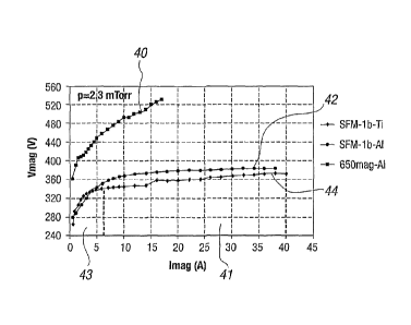
Referring to Figure 4, there is shown a graph which illustrates
the manner in which power can be applied to the magnetron in
accordance with the invention. In this case, it is shown in line
40 for a conventional magnetron that as the current increases so
the voltage increases which causes damaged coatings to be
created. However the graph lines 42, 44 which represent the
use of magnetrons in accordance with the invention show how
CA 02660085 2013-07-03
17
in the initial phase of operation 43 from start the current and
voltage increase at a similar rate and thereafter, in the phase 41,
the current increases without the matching increase in the
voltage, so it is the current which is increased in particular
thereby allowing the application of relatively high power levels
to the Magnetron, with relatively low voltage values. The ability
to kept the voltage levels relatively low avoids damage to the
coatings while the increase in current and hence the power level
allows increased coating speeds to be achieved. This allows
increased power to be achieved in relation to the magnetron,
hence increasing the deposition rate but without causing a
reduction in the quality of coating which is achieved.
The increase in the deposition rates which is possible has been
found to be more than 3 times that of the conventional
apparatus and thereby allows the throughput of the coated
articles to be increased and thereby rendering the overall
process economical commercially, especially for the coating of
relatively high volume articles where previously electron beam
-)0
coating techniques would have been used.
"Iwo examples of coating apparatus which can be used in
accordance with the invention are shown in Figures 5 and 6
respectively. In
Figure 5, there is illustrated an in-line coating
apparatus in which a series of magnetrons 52A,B are provided in
pairs such that, each target in pair 52A is of the same material
and each target in pair 52B is of the same material. Thus
the
material which is deposited from the targets in any given pair,
allow the application of a similar coating to opposing faces
56,58 of the substrate 54 as they are passed through the coating
chamber 60 in the direction of arrows 62. The in-
line coating
apparatus allows the relatively high rate deposition of material
onto the faces of the substrates.
CA 02660085 2013-07-03
18
Figure 6 illustrates an alternative coating arrangement in plan.
In this case the coating chamber 70 is provided with a series of
magnetrons 72 spaced around the same. Substrate carrier 64 is
provided to rotate as indicated by arrow 66 so as to allow
substrates (not shown) mounted on the external surface 68 of
the carrier 64, to be rotated past each of the magnetrons 72
which can be selectively operated to sputter material from the
targets mounted thereon at any given time. In one
embodiment, the magnetrons may be provided as part of a
closed field unbalanced magnetron sputter ion plating apparatus.
A schematic representation of an experimental apparatus for the
magnetron testing is shown on Fig. 7. The coating chamber 70
has a diameter of 650 mm and height 600 mm. Prior to
)5
experiments it was pumped by a Leybold T-1600 turbopump
typically to 6.7.10 Pa base pressure. Gas pressure in the
chamber was set by regulating gas flow by MKS mass-flow
controllers. In these experiments argon flow was regulated
between 7.5 and 75 sccm. When the magnetron was operated
with a Ti target nitrogen flow was set at approximately 0.6 that
of the argon flow to verify operation of the magnetron (HPM)
during the reactive process.
Two unbalanced high power magnetrons (RPM) 72 in
accordance with the invention were used with standard
industrial size rectangular targets 380mm by 175 mm were
mounted opposite each other in the chamber. They formed a
closed field magnetic configuration. The magnetrons differ from
the conventional magnetron (CM) by a stronger magnetic field
above the target and optimised water cooling system. They were
powered by Advanced Energy MDX-11 DC generators, capable
of producing up to 15 kW output power. When current-voltage
characteristics were recorded, one HPM was operated at a time
with the generator run in current regulation mode.
CA 02660085 2009-02-05
WO 2008/007095
PCT/GB2007/002600
19
The optical emission spectra (OES) were recorded through a
viewport at the top lid of the chamber using EP200 Verity
Instruments monochromator. The line of sight of the viewport,
covered by the fused quartz window, was passing at 20 mm from
the magnetron target above the longer side of its sputter track.
During deposition of the TiN coating, nitrogen supply in the
chamber was regulated by a piezo valve, driven by a controller
linked with optical emission monitor, which was set at 497 nm
emission line of titanium. Coating properties were studied using
a Fischerscope H100 hardness tester and TCL ST-3001 Tribo
tester in the mode of unidirectional scratch.
The current-voltage characteristics of the high-power magnetron
with aluminium target are presented in Fig. 8. Pressure change
from 0.09 to 0.7 Pa did not affect significantly the shape of the
curves. With the increase of the discharge current the cathode
voltage saturates starting from 16 A, staying practically flat up
to the maximum output power of the DC generator. At 0.17 Pa
the cathode voltage had a weak maximum 278 V with its value
dropping by 5 V above 30 A current on the target. On the
contrary the cathode voltage of the standard magnetron did not
saturate with current increase, significantly exceeding the
cathode voltage of the HPM run at the same pressure of 0.3 Pa.
The current-voltage characteristics of an HPM with a titanium
target are presented in Fig.9. Saturation of the cathode voltage
occurred at around 4 to 6 A, then the voltage rises slightly as the
current is increased. Small humps can also be seen in both
plots. This complex nature of the curves is linked with the
formation of a nitride layer on the target surface, which is
sputtered away at the higher values of current. Examination
after opening the deposition chamber revealed a surface of the
erosion track having a silvery metallic colour surrounded by a
CA 02660085 2009-02-05
WO 2008/007095
PCT/GB2007/002600
characteristic yellow deposit on the unsputtered parts of the
target .
Current-voltage characteristics of the HPM and Conventional
magnetron (CM) with graphite targets are presented on Fig. 10.
They demonstrate the same tendency as during the runs with the
aluminium target. The HPM curve displays a much slower rise
of voltage with current increase in comparison with the
conventional magnetron (CM) and allows operation of graphite
target at higher power levels without arcing occurring.
Operation of the HPM at powers up to 15 kW draws
significantly higher current to the samples as shown in Figure
11. Current to the samples from HPM plasmas increases
starting from 1.5 kW on the target, while in the case of
conventional magnetron it increases straightaway. It may be
attributed to a better confinement of plasma above the HPM
target at low discharge power due to its stronger magnetic field.
Further, almost linear growth of the current occurs for both
magnetrons with the current from HPM plasma 2.5 times
exceeding the one from the conventional magnetron.
OES spectrum were recorded during operation of the HPM with
an aluminium target at 2.2 kW power characteristic to deposition
processes with conventional magnetron, and 8.6 kW and are
shown in Figure 12. At the low power the most prominent
peaks are with their maximum at 308 and 395 nm, which are
associated with emission lines of All atoms 308.2, 309.3, 394.4
and 396.2nm. At the high power they continue to dominate the
spectrum with growth of the AlI lines at 257.5 and 266 nm. Also
Ad lines at 415.9, 425.9, 430 and 433.4 nm become quite
noticeable. Appearance of the emission lines at 281.5 and 358.7
nm, corresponding to the transitions of AlII ions, indicates
partial ionisation of the sputtered material. But their small value
CA 02660085 2009-02-05
WO 2008/007095
PCT/GB2007/002600
21 =
in comparison with the lines of neutral aluminium points out
that conventional sputtering by argon ions dominates the
process. Substantial input of self-sputtering mode could be
expected at power density around 300 W/cm2 on the target.
Trial deposition run of TiN coating was conducted using two
unbalanced HPMs (Fig. 7) powered by 12 kW each. M42 tool
steel samples were mounted on the ring sample holder (Fig. 7),
which rotated at 4 rev/min. Separation from the magnetron
targets, when samples were passing in front of it, was 15 cm.
Resulting coating had hardness 33 GPa and good adhesion
properties. No delamination of the coating was observed in the
scratch track up to 60 N maximum load. No droplets could be
detected by SEM on the coating surface. Total thickness,
measured by ball crater method, was 3.36 p,m, which gave
deposition rate 4 vim/h. For comparison, in a conventional
magnetron system at 6 kW net power TiN coating is deposited at
1-1.2 ilm/h. These results demonstrate that deposition rates
could be increased in comparison with conventional magnetron
processes proportionally to the power applied to the sputter
target. Also, rates of coating from HPM approach those
obtained from arc evaporation technique.
The magnetrons in accordance with the invention in another
example are operated at power up to 15 kW with power density
on the target up to 40 W/cm2, which is more than 3.5 times that
of the conventional magnetron. The current-voltage
characteristics indicate that much higher power could be used.
The deposition rate of the magnetron rival that of arc sources
but without the associated droplet formation.
In a further set of trials relating to coatings formed using the
magnetron (RPM), the following was performed. Coatings were
CA 02660085 2009-02-05
WO 2008/007095
PCT/GB2007/002600
22
deposited in a Teer UDP650/4 closed field unbalanced
magnetron sputtering system with four magnetrons. For all
coatings, the deposition chamber was configured with two
carbon targets (opposite one another) and two chromium
targets. Each UDP650 target was 345 x145mm, mounted on a
380 x 175mm copper backing plate. Initially, the sputtering
system was used with conventional magnetrons, to deposit
coatings at 3.5A current input to the carbon targets, (i.e. at
maximum power input possible for stable operation: 2.4 kW, 36
kWm-2). DC power was used on the targets and substrates were
biased with a pulsed DC supply. A typical coating sequence was
used, i.e. ion cleaning, deposition of a Cr adhesion layer, then
deposition of a Cr/C graded layer to .change composition from
pure chromium to the composition of the tribological coating
(carbon containing -7 at% Cr). Parameters are then kept
constant until the end of the process. Test pieces coated were
M42 high speed steel, ground to a 1200 SiC finish and cleaned
ultrasonically in acetone before coating.
For the high deposition rate coatings, two HPMs were used to
replace the conventional magnetrons supporting the carbon
targets. The HPM design included redesigned water cooling
cavities to promote more efficient target cooling, and a stronger
magnetic arrangement than that used previously. The
magnetrons used for the chromium targets were not changed.
Prior to loading any samples, the HPM magnetrons were
operated at different powers, and the current - voltage
characteristics recorded. It was found possible to sputter the
carbon targets, without instability, at currents up to 12A (560 to
590V) and target powers up to -7kW (104kWm1 compared to
the 2.4 kW (36 kWin-2) achieved previously.
Substrates were loaded into the chamber, and coated with pure
carbon, using high target currents (9A to 12A) to establish
CA 02660085 2009-02-05
WO 2008/007095
PCT/GB2007/002600
23
carbon deposition rates. Required increases in chromium target
power were then estimated based on the carbon deposition rates
achieved. Coating trials were then carried out at the higher
carbon and chromium target current values, using the deposition
procedure described above, although deposition times for the
final layer were reduced to achieve a coating of the required
thickness. Tribological tests (detailed below) were used to assess
coating performance. Further coatings were then produced at
different carbon target current values from 2.5A (1.1 kW) to
12A (7kW), to assess the suitability of the HPMs for use over a
range of target powers. The ion current at the sample fixture
was monitored during all coating process runs.
Optical microscopy was used to examine the surface of the
coatings, and to study wear tracks following tribological testing.
Coating thicknesses were assessed using the ball crater taper-
section technique. A standard hardness tester (Wilson/Rockwell
B503-R) using a load of 150kgf was used to assess the adhesion
of the coatings. The plastic microhardness was determined using
a Fischerscope H100 ultramicro-hardness tester with a Vickers
indenter, from the load penetration curves. Data from five
indents made on each sample were averaged. The
loading/unloading rate was 10mNs-1, with a maximum applied
load of 50mN.
A Teer POD-2 pin-on-disc tester was used to assess the
tribological performance of the coatings against a 5mm diameter
WC/6/0 Co ball under 80N applied normal load. Tests were
performed at 200mms-1 linear speed on an 8mm diameter wear
track, for a sliding distance of 360m. All tests were unlubricated
and at room temperature (-25 C) and relative humidity (-35%).
The friction coefficient was monitored using a strain-gauge load
cell, and the wear volume measured by producing a ball crater
taper-section on the wear track. The wear volume was then
CA 02660085 2009-02-05
WO 2008/007095
PCT/GB2007/002600
24
normalised with respect to the load and sliding speed to give
specific wear rates.
Coating structures were analysed by X-ray Diffraction using a
Philips PW 1070/30 instrument and 0/20 (Bragg-Brentano)
configuration. Cu Ka radiation source, 40kV and 35mA on the
target, was used for the measurement. Scan conditions were: 20
range of 20-100'; step scan: 0.02 /step, 0.4sec./step; a Graphite
monochromater was used; slit combination 1 -0.5 -0.5-1. The
approximate chemical compositions of samples were obtained
using Glow Discharge Spectroscopy (GDS) in a LECO GDS-750
QDP apparatus.
Figure 13 shows the current-voltage curves obtained for each of
the high power magnetrons tested, compared with the curve for
a conventional magnetron. For the new design of magnetron,
large increases in target current are obtained with only small
increases in target voltage, allowing it to be operated at much
higher target powers without introducing instabilities such as
arcing. Ion current values recorded on the test piece sample
fixture during deposition of the high power coatings were
significantly higher (x2.5 to x3.5) than for the 3.5A coating as
would be expected. This is due to the high flux of ions and
electrons from the unbalanced magnetron, which increases as
the power input is increased. The sample fixture was the same
for all three tests hence it can be assumed that the ion current
density has increased significantly. Although, temperatures at
the substrate fixture were not monitored during these trials, it
can be assumed that these higher ion current densities would
have resulted in higher substrate temperatures, and this would
need to be considered when assessing the suitability of the high
power process to coat temperature sensitive materials.
Operation of the HPM at lower powers resulted in similar ion
CA 02660085 2009-02-05
WO 2008/007095
PCT/GB2007/002600
current values to those normally seen for the conventional
magnetron at those powers.
Table I shows the coating thickness measurements and relative
deposition rates for the standard coating, and two of coatings
produced at much higher power with the new magnetron design.
Table I: Comparative coating deposition rates.
Magnetron Carbon Coating thickness Deposition Deposition
Design target Cr Graphit- Total Time rate
current in.terlayer iC / gm Graphit- Graphit-
/A /gm / jim iC/ hrs iC/
m/hr
Conventional 3.5 0.2 1.8 - 2.0 2.0-2.2 4 0.45 -
0.5
RPM 9.0 0.2 1.8 - 1.9 2.0-2.1 2 0.9 ¨
0.95
HPM 12.0 0.2 2.4/2.5 2.6/2.7 2 1.2
/1.35
It can be seen that the deposition rate has been increased by up
to 2.7 times depending on the operating conditions chosen. This
enables the deposition time to be more than halved. These times
are for the particular size of target used in the UDP650 system
which is a relatively small production system or large R&D
system. Deposition rates in larger production systems, often
with six larger targets, are twice that of the smaller systems, and
should the same designs be applied to the magnetrons in these,
deposition rates could again be increased.
CA 02660085 2009-02-05
WO 2008/007095
PCT/GB2007/002600
26
All coatings produced demonstrated good adhesion to the M42
substrate: Rockwell indentations produced in the coatings were
classed as HF1 to HF2. Figures 14a-b shows the surface quality
of the HPM coatings. The 9A coatings (Fig. 14a) showed very
little evidence of spots or defects and generally appeared better
than typically seen for 3.5A coatings produced with
conventional magnetrons. The surface quality of the 12A coating
(Fig.14b) appeared comparable to that usually seen for a 3.5A
coating. i.e. a very low level of surface defects were visible. The
plastic hardness values were 1519 to 1729 kgmm-2 for the 9A
coatings, and 1554 kgmm-2 for the 12A coating. This compares
to 1769 kgmm' obtained for the 3.5A coating with Hardness
values typically ranging from 1500 kgmm-2 to 1700 kgmm-2 in
this coating system.
Pin-on-disc tests as indicated in Figures 15a-c, under high (80N)
load confirmed that the coatings had similar characteristics to
those produced at lower power, as shown in Figure 16,
demonstrating the same high load bearing capability and low
friction characteristics. Wear rates measured on taper cross-
sections produced by ball cratering on the wear tracks were <3 x
10-17m3/Nm and friction coefficients were 0.07/0.08 for 9A
coatings and 0.09 for the 12A coating. This data and the results
from the hardness tests, suggest that coatings produced in
reduced deposition times should offer the same wear resistance
to components operating in air as currently achievable with
typical coatings.
Table II shows that the HPMs can also be operated at lower
target powers and currents if coatings are required on more
temperature sensitive substrates.
CA 02660085 2009-02-05
WO 2008/007095
PCT/GB2007/002600
27
Table II : Wear properties of coatings produced with the HPM
at different currents.
Magnetron C Cr Target Specific Final
Design Target Current**/A Wear Friction
Current Rate at Coefficient
*/ A 80N
POD/
N3 -ina-i
Conventional 3.5 0.25 2.1 x10-1.7 0.07
HPM 2.5 0.18 2.7 x10⁻¹⁷ 0.07
HPM 5.0 0.25 3.3 x10⁻¹⁷ 0.08
HPM 9.0 0.40 2.8 x10⁻¹⁷ 0.08
HPM 12.0 0.54 2.9 x 10⁻¹⁷ 0.09
* applied to each of two carbon targets
* applied to one of two chromium targets
X-ray diffraction of 9A and 12A coatings produced traces
identical to that for the 3.5A coating, showing only peaks
characteristic of uncoated M42 high speed steel substrates. No
other peaks could be identified suggesting that all three coatings
had the same amorphous structure characteristic of the
conventional formed coatings.
Analysis by GDS showed the chromium content to fall from
approximately 6a0/0 for the 3.5A coating to around 3a0/0 and
1 at% for the 9A and 12A coatings respectively, suggesting that
the Cr content was lower within the coatings sputtered at faster
rates. The chromium target powers chosen were based on the
pure carbon deposition rates obtained, and assumption that the
chromium sputter rate would increase linearly with power input
to the target. However, factors such as cross-contamination of
targets and increased ionization within the chamber may have
also influenced the chromium sputter rate. The lower chromium
CA 02660085 2009-02-05
WO 2008/007095
PCT/GB2007/002600
28
content was not found to be detrimental to the toughness and
load bearing capability of the coating, but future work should
investigate variations to Cr content.
Coatings were produced by sputtering carbon targets from a new
magnetron design, with stronger magnetic field and enhanced
target cooling. Operation of the high power magnetrons was
possible at approximately three times the power input achievable
with conventional designs, and this enabled sputter rates to be
increased by up to 2.7 times and deposition times to be
significantly reduced. Tribological and physical properties of the
coatings deposited were not found to be greatly influenced by
the fast deposition rates and coatings produced demonstrated
good wear rates of <5x10-17 na3/Nm when tested in atmospheric
conditions against WC /6wt%Co counterfaces at high (80N)
load.
Properties of the coatings such as surface quality and adhesion
of the coatings whci are achieved using the apparatus and
method of the invention are found to be good hence allowing
the application of coatings onto articles such as plates for fuel
cells to be achieved using sputtering rather than electron beam
techniques. The reduction in process times achievable with the
use of the magnetrons in accordance with the invention is an
important factor in the drive to advance process efficiency,
economic aspects and suitability for a wider range of
applications.
The provision of coatings of the graphitic type as herein
described onto articles which require conductivity and wear
resistance but without the need for high priced inert metals to
be used also represents a significant development in the
manufacture of this type of article.