Note: Descriptions are shown in the official language in which they were submitted.
CA 02660367 2015-03-13
WO 2008/021913 PCT/US2007/075522
-1-
METHOD AND SYSTEM FOR PROVIDING CALIBRATION OF AN
ANALYTE SENSOR IN AN ANALYTE MONITORING SYSTEM
PRIORITY
This PCT Application claims priority to United States Patent Application No.
11/463,582, filed August 9, 2006 titled "Method and System for Providing
Calibration of an Analyte Sensor in an Analyte Monitoring System".
BACKGROUND
Analyte, e.g., glucose monitoring systems including continuous and discrete
monitoring systems generally include a small, lightweight battery powered and
microprocessor controlled system which is configured to detect signals
proportional
to the corresponding measured glucose levels using an electrometer, and RF
signals
to transmit the collected data. One aspect of certain analyte monitoring
systems
include a transcutaneous or subcutaneous analyte sensor configuration which
is, for
example, partially mounted on the skin of a subject whose analyte level is to
be
monitored. The sensor cell may use a two or three-electrode (work, reference
and
counter electrodes) configuration driven by a controlled potential
(potentiostat)
analog circuit connected through a contact system.
To obtain accurate data from the analyte sensor, calibration is necessary.
Typically, blood glucose measurements are periodically obtained using, for
example,
a blood glucose meter, and the measured blood glucose values are used to
calibrate
the sensors. Indeed, the patient must calibrate each new analyte sensor using
for
example, capillary blood glucose measurements. This may be inconvenient for
the
patient.
In view of the foregoing, it would be desirable to have a method and system
for calibrating analyte sensors of an analyte monitoring system that does not
inconveniently require periodic blood glucose measurements for sensor
calibration.
CA 02660367 2009-02-06
WO 2008/021913
PCT/US2007/075522
-2-
SUMMARY OF THE INVENTION
In view of the foregoing, in accordance with the various embodiments of the
present invention, there is provided a method and system for providing
substantially
automatic and substantially real time calibration of analyte sensors for use
in an
analyte monitoring system.
These and other objects, features and advantages of the present invention will
become more fully apparent from the following detailed description of the
embodiments, the appended claims and the accompanying drawings.
BRIEF DESCRIPTION OF THE DRAWINGS
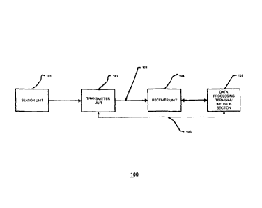
FIG. 1 illustrates a block diagram of a data monitoring and management
system for practicing one embodiment of the present invention;
FIG. 2 is a block diagram of the transmitter unit of the data monitoring and
management system shown in FIG. 1 in accordance with one embodiment of the
present invention;
FIG. 3 is a block diagram of the receiver/monitor unit of the data monitoring
and management system shown in FIG. 1 in accordance with one embodiment of the
present invention;
FIG. 4 is a flowchart illustrating analyte sensor sensitivity estimation
procedure in accordance with one embodiment of the present invention;
FIG. 5 is a flowchart illustrating the analyte sensor sensitivity estimation
procedure in accordance with another embodiment of the present invention;
FIG. 6 is a flowchart illustrating an analyte sensor parameter estimation
procedure in accordance with one embodiment of the present invention;
FIG. 7A illustrates the transmission of the control signal from the
transmitter
processor in accordance with one embodiment of the present invention;
FIG. 7B illustrates the measured response to the control signal from the
transmitter processor shown in FIG. 7A in accordance with one embodiment of
the
present invention;
CA 02660367 2009-02-06
WO 2008/021913
PCT/US2007/075522
-3-
FIG. 8 is a tabular illustration of a lookup table for sensor sensitivity for
use
with the calibration procedure in accordance with one embodiment of the
present
invention; and
FIG. 9 is a flowchart illustrating the analyte sensor sensitivity estimation
procedure in accordance with another embodiment of the present invention.
DETAILED DESCRIPTION
As described in detail below, in accordance with the various embodiments of
the present invention, there is provided a method and system for determining
sensor
sensitivity of an analyte sensor which may be used to calibrate the analyte
sensor in
the analyte monitoring system. In particular, within the scope of the present
invention, there is provided method and system for automatically calibrating
subcutaneous or transcutaneously positioned analyte sensors such that the
frequency
of capillary blood glucose measurement for calibration of the sensors may be
minimized.
More specifically, FIG. 1 illustrates a data monitoring and management
system such as, for example, analyte (e.g., glucose) monitoring system 100 in
accordance with one embodiment of the present invention. The subject invention
is
further described primarily with respect to a glucose monitoring system for
convenience and such description is in no way intended to limit the scope of
the
invention. It is to be understood that the analyte monitoring system may be
configured to monitor a variety of analytes, e.g., lactate, and the like.
Analytes that may be monitored include, for example, acetyl choline, amylase,
bilirubin, cholesterol, chorionic gonadotropin, creatine kinase (e.g., CK-MB),
creatine, DNA, fructosamine, glucose, glutamine, growth hormones, hormones,
ketones, lactate, peroxide, prostate-specific antigen, prothrombin, RNA,
thyroid
stimulating hormone, and troponin. The concentration of drugs, such as, for
example,
antibiotics (e.g., gentamicin, vancomycin, and the like), digitoxin, digoxin,
drugs of
abuse, theophylline, and warfarin, may also be monitored.
CA 02660367 2009-02-06
WO 2008/021913
PCT/US2007/075522
-4-
The analyte monitoring system 100 includes a sensor 101, a transmitter unit
102 coupled to the sensor 101, and a receiver unit 104 which is configured to
communicate with the transmitter unit 102 via a communication link 103. The
receiver unit 104 may be further configured to transmit data to a data
processing
terminal 105 for evaluating the data received by the receiver unit 104.
Moreover, the
data processing terminal in one embodiment may be configured to receive data
directly from the transmitter unit 102 via a communication liffl( 106 which
may
optionally be configured for bi-directional communication.
Only one sensor 101, transmitter unit 102, receiver unit 104, communication
link 103, and data processing terminal 105 are shown in the embodiment of the
analyte monitoring system 100 illustrated in FIG. 1. However, it will be
appreciated
by one of ordinary skill in the art that the analyte monitoring system 100 may
include
one or more sensor 101, transmitter unit 102, receiver unit 104, communication
link
103, and data processing terminal 105. Moreover, within the scope of the
present
invention, the analyte monitoring system 100 may be a continuous monitoring
system, or semi-continuous, or a discrete monitoring system. In a multi-
component
environment, each device is configured to be uniquely identified by each of
the other
devices in the system so that communication conflict is readily resolved
between the
various components within the analyte monitoring system 100.
In one embodiment of the present invention, the sensor 101 is physically
positioned in or on the body of a user whose analyte level is being monitored.
The
sensor 101 may be configured to continuously sample the analyte level of the
user
and convert the sampled analyte level into a corresponding data signal for
transmission by the transmitter unit 102. In one embodiment, the transmitter
unit 102
is mounted on the sensor 101 so that both devices are positioned on the user's
body.
The transmitter unit 102 performs data processing such as filtering and
encoding on
data signals, each of which corresponds to a sampled analyte level of the
user, for
transmission to the receiver unit 104 via the communication link 103.
In one embodiment, the analyte monitoring system 100 is configured as a one-
way RF communication path from the transmitter unit 102 to the receiver unit
104. In
CA 02660367 2009-02-06
WO 2008/021913
PCT/US2007/075522
-5-
such embodiment, the transmitter unit 102 transmits the sampled data signals
received
from the sensor 101 without acknowledgement from the receiver unit 104 that
the
transmitted sampled data signals have been received. For example, the
transmitter
unit 102 may be configured to transmit the encoded sampled data signals at a
fixed
rate (e.g., at one minute intervals) after the completion of the initial power
on
procedure. Likewise, the receiver unit 104 may be configured to detect such
transmitted encoded sampled data signals at predetermined time intervals.
Alternatively, the analyte monitoring system 100 may be configured with a bi-
directional RF (or otherwise) communication between the transmitter unit 102
and the
receiver unit 104.
Additionally, in one aspect, the receiver unit 104 may include two sections.
The first section is an analog interface section that is configured to
communicate with
the transmitter unit 102 via the communication liffl( 103. In one embodiment,
the
analog interface section may include an RF receiver and an antenna for
receiving and
amplifying the data signals from the transmitter unit 102, which are
thereafter,
demodulated with a local oscillator and filtered through a band-pass filter.
The
second section of the receiver unit 104 is a data processing section which is
configured to process the data signals received from the transmitter unit 102
such as
by performing data decoding, error detection and correction, data clock
generation,
and data bit recovery.
In operation, upon completing the power-on procedure, the receiver unit 104
is configured to detect the presence of the transmitter unit 102 within its
range based
on, for example, the strength of the detected data signals received from the
transmitter
unit 102 or a predetermined transmitter identification information. Upon
successful
synchronization with the corresponding transmitter unit 102, the receiver unit
104 is
configured to begin receiving from the transmitter unit 102 data signals
corresponding to the user's detected analyte level. More specifically, the
receiver unit
104 in one embodiment is configured to perform synchronized time hopping with
the
corresponding synchronized transmitter unit 102 via the communication link 103
to
obtain the user's detected analyte level.
CA 02660367 2009-02-06
WO 2008/021913
PCT/US2007/075522
-6-
Referring again to FIG. 1, the data processing terminal 105 may include a
personal computer, a portable computer such as a laptop or a handheld device
(e.g.,
personal digital assistants (PDAs)), and the like, each of which may be
configured for
data communication with the receiver via a wired or a wireless connection.
Additionally, the data processing terminal 105 may further be connected to a
data
network (not shown) for storing, retrieving and updating data corresponding to
the
detected analyte level of the user.
Within the scope of the present invention, the data processing terminal 105
may include an infusion device such as an insulin infusion pump or the like,
which
may be configured to administer insulin to patients, and which may be
configured to
communicate with the receiver unit 104 for receiving, among others, the
measured
analyte level. Alternatively, the receiver unit 104 may be configured to
integrate an
infusion device therein so that the receiver unit 104 is configured to
administer
insulin therapy to patients, for example, for administering and modifying
basal
profiles, as well as for determining appropriate boluses for administration
based on,
among others, the detected analyte levels received from the transmitter unit
102.
Additionally, the transmitter unit 102, the receiver unit 104 and the data
processing terminal 105 may each be configured for bi-directional wireless
communication such that each of the transmitter unit 102, the receiver unit
104 and
the data processing terminal 105 may be configured to communicate (that is,
transmit
data to and receive data from) with each other via the wireless communication
link
103. More specifically, the data processing terminal 105 may in one embodiment
be
configured to receive data directly from the transmitter unit 102 via the
communication liffl( 106, where the communication liffl( 106, as described
above, may
be configured for bi-directional communication.
In this embodiment, the data processing terminal 105 which may include an
insulin pump, may be configured to receive the analyte signals from the
transmitter
unit 102, and thus, incorporate the functions of the receiver 103 including
data
processing for managing the patient's insulin therapy and analyte monitoring.
In one
embodiment, the communication link 103 may include one or more of an RF
CA 02660367 2009-02-06
WO 2008/021913
PCT/US2007/075522
-7-
communication protocol, an infrared communication protocol, a Bluetooth
enabled
communication protocol, an 802.11x wireless communication protocol, or an
equivalent wireless communication protocol which would allow secure, wireless
communication of several units (for example, per HIPPA requirements) while
avoiding potential data collision and interference.
FIG. 2 is a block diagram of the transmitter of the data monitoring and
detection system shown in FIG. 1 in accordance with one embodiment of the
present
invention. Referring to the Figure, the transmitter unit 102 in one embodiment
includes an analog interface 201 configured to communicate with the sensor 101
(FIG. 1), a user input 202, and a temperature detection section 203, each of
which is
operatively coupled to a transmitter processor 204 such as a central
processing unit
(CPU). As can be seen from FIG. 2, there are provided four contacts, three of
which
are electrodes - work electrode, guard contact, reference electrode, and
counter
electrode, each operatively coupled to the analog interface 201 of the
transmitter unit
102 for connection to the sensor unit 201 (FIG. 1). In one embodiment, each of
the
work electrode, guard contact, reference electrode, and counter electrode may
be
made using a conductive material that is either printed or etched, for
example, such as
carbon which may be printed, or metal foil (e.g., gold) which may be etched.
Further shown in FIG. 2 are a transmitter serial communication section 205
and an RF transmitter 206, each of which is also operatively coupled to the
transmitter processor 204. Moreover, a power supply 207 such as a battery is
also
provided in the transmitter unit 102 to provide the necessary power for the
transmitter
unit 102. Additionally, as can be seen from the Figure, clock 208 is provided
to,
among others, supply real time information to the transmitter processor 204.
In one embodiment, a unidirectional input path is established from the sensor
101 (FIG. 1) and/or manufacturing and testing equipment to the analog
interface 201
of the transmitter unit 102, while a unidirectional output is established from
the
output of the RF transmitter 206 of the transmitter unit 102 for transmission
to the
receiver unit 104. In this manner, a data path is shown in FIG. 2 between the
aforementioned unidirectional input and output via a dedicated liffl( 209 from
the
CA 02660367 2009-02-06
WO 2008/021913
PCT/US2007/075522
-8-
analog interface 201 to serial communication section 205, thereafter to the
processor
204, and then to the RF transmitter 206. As such, in one embodiment, via the
data
path described above, the transmitter unit 102 is configured to transmit to
the receiver
unit 104 (FIG. 1), via the communication link 103 (FIG. 1), processed and
encoded
data signals received from the sensor 101 (FIG. 1). Additionally, the
unidirectional
communication data path between the analog interface 201 and the RF
transmitter
206 discussed above allows for the configuration of the transmitter unit 102
for
operation upon completion of the manufacturing process as well as for direct
communication for diagnostic and testing purposes.
As discussed above, the transmitter processor 204 is configured to transmit
control signals to the various sections of the transmitter unit 102 during the
operation
of the transmitter unit 102. In one embodiment, the transmitter processor 204
also
includes a memory (not shown) for storing data such as the identification
information
for the transmitter unit 102, as well as the data signals received from the
sensor 101.
The stored information may be retrieved and processed for transmission to the
receiver unit 104 under the control of the transmitter processor 204.
Furthermore, the
power supply 207 may include a commercially available battery.
The transmitter unit 102 is also configured such that the power supply section
207 is capable of providing power to the transmitter for a minimum of about
three
months of continuous operation after having been stored for about eighteen
months in
a low-power (non-operating) mode. In one embodiment, this may be achieved by
the
transmitter processor 204 operating in low power modes in the non-operating
state,
for example, drawing no more than approximately 1 ilA of current. Indeed, in
one
embodiment, the final step during the manufacturing process of the transmitter
unit
102 may place the transmitter unit 102 in the lower power, non-operating state
(i.e.,
post-manufacture sleep mode). In this manner, the shelf life of the
transmitter unit
102 may be significantly improved.
Moreover, as shown in FIG. 2, while the power supply unit 207 is shown as
coupled to the processor 204, and as such, the processor 204 is configured to
provide
CA 02660367 2009-02-06
WO 2008/021913
PCT/US2007/075522
-9-
control of the power supply unit 207, it should be noted that within the scope
of the
present invention, the power supply unit 207 is configured to provide the
necessary
power to each of the components of the transmitter unit 102 shown in FIG. 2.
Referring back to FIG. 2, the power supply section 207 of the transmitter unit
102 in one embodiment may include a rechargeable battery unit that may be
recharged by a separate power supply recharging unit (for example, provided in
the
receiver unit 104) so that the transmitter unit 102 may be powered for a
longer period
of usage time. Moreover, in one embodiment, the transmitter unit 102 may be
configured without a battery in the power supply section 207, in which case
the
transmitter unit 102 may be configured to receive power from an external power
supply source (for example, a battery) as discussed in further detail below.
Referring yet again to FIG. 2, the temperature detection section 203 of the
transmitter unit 102 is configured to monitor the temperature of the skin near
the
sensor insertion site. The temperature reading is used to adjust the analyte
readings
obtained from the analog interface 201. The RF transmitter 206 of the
transmitter
unit 102 may be configured for operation in the frequency band of 315 MHz to
322
MHz, for example, in the United States. Further, in one embodiment, the RF
transmitter 206 is configured to modulate the carrier frequency by performing
Frequency Shift Keying and Manchester encoding. In one embodiment, the data
transmission rate is 19,200 symbols per second, with a minimum transmission
range
for communication with the receiver unit 104.
Additional detailed description of the continuous analyte monitoring system,
its various components including the functional descriptions of the
transmitter are
provided in U.S. Patent No. 6,175,752 issued January 16, 2001 entitled
"Analyte
Monitoring Device and Methods of Use", and in application No. 10/745,878 filed
December 26, 2003 entitled "Continuous Glucose Monitoring System and Methods
of
Use", each assigned to the Assignee of the present application.
FIG. 3 is a block diagram of the receiver/monitor unit of the data monitoring
and management system shown in FIG. 1 in accordance with one embodiment of the
present invention. Referring to FIG. 3, the receiver unit 104 includes a blood
glucose
CA 02660367 2009-02-06
WO 2008/021913
PCT/US2007/075522
-10-
test strip interface 301, an RF receiver 302, an input 303, a temperature
detection
section 304, and a clock 305, each of which is operatively coupled to a
receiver
processor 307. As can be further seen from the Figure, the receiver unit 104
also
includes a power supply 306 operatively coupled to a power conversion and
monitoring section 308. Further, the power conversion and monitoring section
308 is
also coupled to the receiver processor 307. Moreover, also shown are a
receiver
serial communication section 309, and an output 310, each operatively coupled
to the
receiver processor 307.
In one embodiment, the test strip interface 301 includes a glucose level
testing
portion to receive a manual insertion of a glucose test strip, and thereby
determine
and display the glucose level of the test strip on the output 310 of the
receiver unit
104. This manual testing of glucose can be used to calibrate sensor 101. The
RF
receiver 302 is configured to communicate, via the communication link 103
(FIG. 1)
with the RF transmitter 206 of the transmitter unit 102, to receive encoded
data
signals from the transmitter unit 102 for, among others, signal mixing,
demodulation,
and other data processing. The input 303 of the receiver unit 104 is
configured to
allow the user to enter information into the receiver unit 104 as needed. In
one
aspect, the input 303 may include one or more keys of a keypad, a touch-
sensitive
screen, or a voice-activated input command unit. The temperature detection
section
304 is configured to provide temperature information of the receiver unit 104
to the
receiver processor 307, while the clock 305 provides, among others, real time
information to the receiver processor 307.
Each of the various components of the receiver unit 104 shown in FIG. 3 is
powered by the power supply 306 which, in one embodiment, includes a battery.
Furthermore, the power conversion and monitoring section 308 is configured to
monitor the power usage by the various components in the receiver unit 104 for
effective power management and to alert the user, for example, in the event of
power
usage which renders the receiver unit 104 in sub-optimal operating conditions.
An
example of such sub-optimal operating condition may include, for example,
operating
the vibration output mode (as discussed below) for a period of time thus
substantially
CA 02660367 2009-02-06
WO 2008/021913
PCT/US2007/075522
-11-
draining the power supply 306 while the processor 307 (thus, the receiver unit
104) is
turned on. Moreover, the power conversion and monitoring section 308 may
additionally be configured to include a reverse polarity protection circuit
such as a
field effect transistor (FET) configured as a battery activated switch.
The serial communication section 309 in the receiver unit 104 is configured to
provide a bi-directional communication path from the testing and/or
manufacturing
equipment for, among others, initialization, testing, and configuration of the
receiver
unit 104. Serial communication section 104 can also be used to upload data to
a
computer, such as time-stamped blood glucose data. The communication liffl(
with an
external device (not shown) can be made, for example, by cable, infrared (IR)
or RF
link. The output 310 of the receiver unit 104 is configured to provide, among
others,
a graphical user interface (GUI) such as a liquid crystal display (LCD) for
displaying
information. Additionally, the output 310 may also include an integrated
speaker for
outputting audible signals as well as to provide vibration output as commonly
found
in handheld electronic devices, such as mobile telephones presently available.
In a
further embodiment, the receiver unit 104 also includes an electro-luminescent
lamp
configured to provide backlighting to the output 310 for output visual display
in dark
ambient surroundings.
Referring back to FIG. 3, the receiver unit 104 in one embodiment may also
include a storage section such as a programmable, non-volatile memory device
as part
of the processor 307, or provided separately in the receiver unit 104,
operatively
coupled to the processor 307. The processor 307 is further configured to
perform
Manchester decoding as well as error detection and correction upon the encoded
data
signals received from the transmitter unit 102 via the communication link 103.
Referring back to the Figures, as described in further detail below, in one
embodiment of the present invention, the transmitter processor 204 may be
configured to transmit a control signal to the analog interface 201 to
determine the
poise voltage between the work electrode and the reference electrode of the
sensor
unit 101, each of which are operatively coupled to the analog interface 201 of
the
transmitter unit 102.
CA 02660367 2009-02-06
WO 2008/021913
PCT/US2007/075522
-12-
More specifically, in one embodiment, a control processor component of the
transmitter unit 102 processor 204 is configured to provide a perturbation
control
signal to the analog interface 201. The analog interface 201 is configured to
translate
the received perturbation control signal to a perturbation that affects the
sensor
response. For example, the control signal in one embodiment may be configured
to
control the voltage level that is applied to the sensor 101 between the work
and
reference electrodes (i.e., the poise voltage). In one embodiment, the analog
interface
201of the transmitter unit 102 is configured to translate the sensor response
to the
perturbation to a corresponding response signal that is acquired by the signal
processing component of the processor 204 of the transmitter unit 102. The
signal
processing component of the processor 204 in the transmitter unit 102 in one
embodiment may be configured to determine the desired sensor parameter
estimation
which is transmitted to the receiver unit 104. Alternatively, the signal
processing
component of the processor 204 in the transmitter unit 102 may be configured
to
preprocess the data, which are then transmitted to the receiver unit for
sensor
parameter estimation determination.
More specifically, FIG. 4 is a flowchart illustrating analyte sensor
sensitivity
estimation procedure in accordance with one embodiment of the present
invention.
Referring to FIG. 4, at step 410, the transmitter processor 204 (FIG. 2) in
one
embodiment is configured to provide a control signal to the analog interface
201 (for
example a poise voltage control circuit) of the transmitter unit 102. In one
aspect, the
control signal provides a perturbation input to determine the poise voltage
between
the work electrode and the reference electrode of the sensor unit 101. In one
aspect,
the poise voltage may be in the range of approximately -600 mV and 600 mV, and
the
analog interface 201 may be configured to control the poise voltage and apply
the
poise voltage to the electrodes of the sensor unit 101.
One embodiment of the control signal perturbations is shown in FIG. 7A
which illustrates the control signal from the transmitter processor 204 so as
to provide
a poise voltage waveform that is a square wave of 50% duty cycle with a one
minute
time period interval. In one embodiment, the poise voltage square wave
amplitude
CA 02660367 2009-02-06
WO 2008/021913
PCT/US2007/075522
-13-
may be switched from 40mV to -600mV from, for example, the normal operating
poise voltage to a predetermined level such as -600 mV which effectively shuts
down
the current signal on the work electrode.
Referring back to FIG, 4, at step 420, the analog interface 201 in one
embodiment is configured to determine a measured response to the received
control
signal, for example, a voltage signal which is substantially proportional to
the current
signal level on the work electrode of the sensor unit 101. An aspect of the
measured
response is illustrated in FIG. 7B. As shown, in one aspect, the current
signal level is
associated with the analyte level of the patient and may be modulated by the
poise
voltage perturbations driven by the control signal from the transmitter
processor 204.
Thereafter at step 430, the transmitter processor 204 may be optionally
configured to
synchronize the measured response from the analog interface 201 with the
control
signal. The transmitter processor 204 may be further configured to store the
measured response and the associated control signal in a storage unit (not
shown)
such as a memory device.
Referring again to FIG. 4, the transmitter processor 204 in one embodiment is
configured to determine the difference or variance in the measured response
based on
the control signal, and the sensor sensitivity may be determined based on the
determined difference in measured response. That is, in one embodiment, the
difference in measured response is compared to a look up table stored, for
example, in
the transmitter processor 204 memory unit which includes calculated measured
response difference for the sensor based on characteristics of the sensor unit
101.
By way of an example, for a measured response difference of 47 analog to
digital counts, the lookup table for sensor sensitivity (FIG. 8) indicates
34.5pA/(mg/dL) for the sensor. Then, the determined sensor sensitivity may be
applied to the work electrode current to determine the corresponding
calibrated
analyte value. That is, the calibrated analyte value may be determined by
dividing the
work electrode current signal by the sensor sensitivity.
FIG. 5 is a flowchart illustrating the analyte sensor sensitivity estimation
procedure in accordance with another embodiment of the present invention.
CA 02660367 2009-02-06
WO 2008/021913
PCT/US2007/075522
-14-
Referring to FIG. 5, at step 510, a perturbation control signal is applied to
the sensor
101 (FIG. 1), and then the response to the perturbation control signal is
measured at
step 520. Based on the measured response to the perturbation control signal,
at step
530 the sensor parameter(s) is estimated and at step 540, the analyte level is
estimated
based on the measured response to the perturbation control signal. In one
embodiment, the procedure shown in FIG. 5 is repeated continuously.
In accordance with the various embodiments of the present invention,
different estimates may be determined including, for example, estimation of
sensor
properties such as sensitivity and response time, the analyte level, and
analyte level
validity/accuracy. In one embodiment, there are several mechanisms that may be
used to perturb the sensor 101 (FIG. 1), for example, the variable poise
voltage. In a
further aspect, the one or more of the perturbation control signals may
include, for
example, square waves. Also, in one aspect, the one or more physical sensor
responses that is measured may include, for example, work electrode current
variation
due to poise voltage perturbation. In addition, signal processing may be used
in one
embodiment to estimate the sensor parameter or analyte level from the sensor
response to the perturbation as described above.
FIG. 6 is a flowchart illustrating an analyte sensor parameter estimation
procedure in accordance with one embodiment of the present invention.
Referring to
FIG. 6, a control signal is applied, for example, to the analog interface 201
of the
transmitter unit 102 (FIG. 1). That is, in one embodiment, the processor 204
of the
transmitter unit 102 may be configured to provide a control signal to a poise
voltage
control circuit (for example, incorporated in the processor 204 of the
transmitter unit
102 as shown in FIG. 2, but which may, in one embodiment, may be separately
provided within the transmitter unit 102) of the transmitter unit 102.
In one aspect, the control signal may be configured to provide a perturbation
input signal to determine the poise voltage between the work electrode and the
reference electrode of the sensor unit 101. In one embodiment, the poise
voltage may
be in the range of approximately -600 mV and 600 mV, and the analog interface
201
CA 02660367 2009-02-06
WO 2008/021913
PCT/US2007/075522
-15-
may be configured to control the poise voltage and apply the poise voltage to
the
electrodes of the sensor unit 101.
As described in further detail below, an embodiment of the control signal
perturbations is shown in FIG. 7A which illustrates the control signal from
the
processor 204 (FIG. 2) to provide a poise voltage waveform that is a square
wave of
50% duty cycle with a one minute time period interval. Referring to FIG. 7A,
in one
embodiment, the poise voltage square wave amplitude may be switched from 40mV
to -600mV from, for example, the normal operating poise voltage to a
predetermined
level such as -600 mV which effectively shuts down the current signal on the
work
electrode.
Referring back to FIG 6, the analog interface 201 in one embodiment is
configured to determine a measured response to the received control signal,
for
example, a voltage signal which is substantially proportional to the current
signal
level on the work electrode of the sensor unit 101 (FIG. 1). As discussed in
further
detail below, one embodiment of the measured response is shown in FIG. 7B.
Referring to FIG. 7B, in one embodiment, the average signal level for half of
the duty
cycle is associated with the analyte level of the patient, but the transient
within the
half-duty cycle period, caused by the poise voltage perturbations driven by
the control
signal from the transmitter processor 204, is associated with the sensitivity
parameter
of the sensor 101. The transmitter processor 204 may be further configured to
store
the measured response and the associated control signal in a storage unit (not
shown)
such as a memory device.
Referring again to FIG. 6, the transmitter processor 204 in one embodiment is
configured to determine the amplitude difference of the transient from the
start of the
half-duty cycle to the end (referred to sometimes as the "on" period) in the
measured
response, and the sensor sensitivity may be determined based on the determined
difference in the response. That is, in one embodiment, the difference in
measured
response is compared to a predetermined sensor parameter such as sensor
sensitivity
that may be stored in a look up table, for example, in the transmitter
processor 204
memory unit. In one aspect, the look up table may include a calculated
measured
CA 02660367 2009-02-06
WO 2008/021913
PCT/US2007/075522
-16-
response difference for the sensor unit 101 and corresponding sensor
sensitivities
based on characteristics of the sensor unit 101.
By way of an example, for a measured response difference of 47 analog to
digital counts, the lookup table for sensor sensitivity as shown in FIG. 8
indicates
34.5pA/(mg/dL) for the sensor. In one embodiment, the transmitter may be
configured to determine this sensitivity value once per minute, and to
transmit the
sensitivity value it to the receiver unit 104 (FIG. 1) in addition to data or
signal
corresponding to the work current signal level, determined at the end of the
"on"
period, and skin temperature.
In one embodiment, the receiver unit 104 (FIG. 1) may be configured to apply
the determined sensor sensitivity to the temperature compensated work
electrode
current signal in order to determine the corresponding calibrated analyte
value or
level. That is, the calibrated analyte value may be determined by dividing the
temperature compensated work electrode current signal by the determined sensor
sensitivity. In one aspect, a time-series of the calibrated analyte values may
be
acquired by the receiver unit 104 (FIG. 1) in real-time, and may be used to
determine
analyte rate-of-change and other analyte signal metrics and/or statistics. In
addition,
the calibrated analyte values may also be used to drive alarms or alerts that
inform the
patient whose analyte is being monitored of analyte level conditions that
require
attention. In addition, in accordance with one aspect of the present
invention, the
receiver unit 104 may be configured to determine whether the sensor
sensitivity range
is within a valid range.
FIG. 7A illustrates the transmission of the control signal from the
transmitter
processor in accordance with one embodiment of the present invention. More
particularly, FIG. 7A illustrates the poise voltage square wave with 50% duty
cycle
with one minute time periods is shown, where the poise voltage square wave
amplitude is switched from 40 mV to -600 mV as in normal operating mode. FIG.
7B
illustrates the measured response to the control signal from the transmitter
processor
shown in FIG. 7A in accordance with one embodiment of the present invention.
More specifically, the measured response which is associated with the analyte
level
CA 02660367 2009-02-06
WO 2008/021913
PCT/US2007/075522
-17-
measured by the sensor unit 101 from the interstitial fluid of a patient as
modulated
by the control signal from the transmitter processor 204 is illustrated with
one minute
time periods
FIG. 8 is a tabular illustration of a lookup table for sensor sensitivity for
use
with the calibration procedure in accordance with one embodiment of the
present
invention. More specifically, in one embodiment, the lookup table shown in
FIG. 8 is
stored in a memory unit (not shown) of the transmitter unit 102 (or
alternatively, in
the transmitter processor 204) and may be accessed by the transmitter
processor 204
to retrieve a corresponding sensitivity value associated with the determined
measured
response difference.
FIG. 9 is a flowchart illustrating the analyte sensor sensitivity estimation
procedure in accordance with another embodiment of the present invention.
Referring to FIG. 9, in one embodiment, a control signal from the transmitter
processor 204 (FIG. 2) is provided to the transmitter unit 102 analog
interface 201,
and a response to the applied control signal is determined. Thereafter, the
difference
or variance in the determined response to the control signal between the
beginning
and end of the half duty cycle is determined. As can be seen, in one
embodiment,
steps 910 to 930 are substantially similar to steps 610 to 630, respectively
described
above.
Referring back to FIG. 9, after determining the measured response variance or
difference between the beginning and end of the half duty cycle, it is
determined
whether the number of transmitted or applied control signals exceed a
predetermined
number or count. If it is determined that the number of transmitted or applied
control
signals do not exceed the predetermined number or count, then a control signal
counter (for example, provided in the transmitter unit 102) is incremented by
one
count, and the routine returns to the beginning where another control signal
is
provided to the analog interface 201 of the transmitter unit 102.
On the other hand, if it is determined that the number of transmitted or
applied
control signals exceed the predetermined number or count, then the sensor
sensitivity
may be determined based on the determined difference in the response. That is,
as
CA 02660367 2009-02-06
WO 2008/021913
PCT/US2007/075522
-18-
discussed above, the difference in measured response in one embodiment is
compared
to a predetermined sensor parameter such as sensor sensitivity that may be
stored in a
look up table, for example, in the transmitter processor 204 memory unit. In
one
aspect, the look up table may include a calculated measured response
difference for
the sensor and corresponding sensor sensitivities based on characteristics of
the
sensor. Furthermore, as discussed above, in one embodiment, the calibrated
analyte
value or level may be determined by, for example, dividing the corresponding
sensor
signal (e.g., work electrode current signal) level by the determined sensor
sensitivity
value.
Within the scope of the present invention, the perturbations to the analyte
sensors may be provided by, for example, altering the poise voltage in time.
Alternatively, an additional electrical current signal may be provided to the
sensor
work or counter electrodes via an AC coupling, where the level of the
additional
electrical current signal may be varied in time by the control signal in a
manner
similar as discussed above. Still in accordance with another embodiment, the
work/counter electrode current path may be opened and closed in a time varying
manner controlled by the control signal. Yet still another embodiment may
provide a
variable resistance in the work/counter electrode current path, where the
variable
resistance is varied in time as controlled by the control signal.
In another aspect of the present invention, the transcutaneously positioned
sensor may be perturbed with a mechanical transducer controlled in time and
amplitude by a predetermined control signal. In one embodiment, mechanical
transducers may include those that can provide physical signals of vibration,
acoustics, thermal or electro-magnetic media, for example. Broadly, any
suitable
mechanism to apply perturbations to the transcutaneously positioned sensor may
be
used to the extent that the measured response may be analyzed by the signal
processing component such as, for example, the transmitter unit processor 204
to
estimate one or more sensor properties based on the signal response induced by
the
perturbations. For example, vibration perturbations may induce fluctuations in
the
sensor membrane that could be detected in the measured response transients,
which
CA 02660367 2009-02-06
WO 2008/021913
PCT/US2007/075522
-19-
may be correlated with membrane thickness and thus provide a measure of the
sensitivity of the sensor.
In addition, in accordance with the various embodiments of the present
invention, there are provided a variety of time-varying controls signals that
may be
applied, along with a variety of techniques used to analyze the measured
response and
estimate the sensor parameter of interest. Some of these control signals may
be
appropriate to induce a measured response that is more informative about a
specific
sensor parameter than other control signals, and some control signals may be
more
practical to implement than others. As discussed previously, a square-wave
control
signal may be employed in one embodiment. Variations in this type of control
signal
may be suitably used where the positive and negative amplitudes are at
different
levels, the duty cycle is other than 50%, or the period is other than 1
minutes.
In another embodiment of the present invention, a feedback mechanism may
be provided where the duty cycle is varied to achieve a desired response, such
as a
specific transient response time. In this case, the final duty cycle is the
parameter that
is correlated with the sensor parameter to be estimated. This feedback
technique may
be extended to other types of control signals, mentioned below, and other
characteristics of the signal such as phase, amplitude and frequency may be
varied to
achieve a desired response.
Alternatively, a sine wave may be used as the control signal discussed above
rather than a square wave. Still alternatively, a series of sine waves at
different
frequencies, or a chirp signal may be used as control signals in one
embodiment of
the present invention. The measured response of these perturbation signals may
then
be analyzed using standard spectral analysis techniques. Based on the spectral
analysis, metrics may be determined that are correlated with the sensor
parameter to
be estimated.
In accordance with yet another embodiment, an impulse signal, or a series of
impulse signals may be alternatively used as control signals. The measured
response
of these perturbation signals may be analyzed using known impulse response
analysis
techniques. For example, the maximum height of the measured response may be
used
CA 02660367 2009-02-06
WO 2008/021913
PCT/US2007/075522
-20-
to determine the associated sensor sensitivity. Alternatively, other signal
metrics
such as the time to reach the maximum height of the measured response, the
area
under the curve of the measured response, the slope of the measured response
may be
correlated with the sensor parameter to be estimated.
In still another embodiment, psuedo-random modulation similar to those used
in spread-spectrum communication systems may be used as the control signals.
The
measured response of these perturbation signals may be analyzed using known
spread-spectrum analysis techniques. Based on this analysis, metrics may be
determined that are correlated with the sensor parameter to be estimated. In
addition,
the response signal may be demodulated using spread-spectrum techniques to
recover
the analyte level.
For some of the control signal/response measurement analysis techniques
discussed above, the relative phase between the control signal and the
measured
response may be used to analyze the measured response to the perturbation. For
some of the control signal/response measurement analysis techniques discussed
above, multiple metrics may be determined. One or more of these metrics may be
used to estimate the sensor parameter of interest. For example, in one
embodiment, a
multidimensional table lookup may be used where one dimension includes the
sensor
parameter of interest, and the other dimensions may each be associated with a
different metric that characterizes the measured response. More specifically,
by way
of illustration, in the impulse response approach described above, both the
maximum
height and the time to reach the height of the measured response may be
determined.
In this case, a three dimensional lookup table may be used.
As discussed above, in one embodiment, a lookup table may be used to
correlate a metric associated with the measured response with a sensor
parameter of
interest (for example, sensitivity). Alternatively, a mathematical function
that relates
the measured response metric with the sensor parameter may be used. The sensor
parameter may then be determined based on the measured response metric as an
input. In another aspect, the estimate of the sensor parameter may be
determined for
many measurements using, for example, the least squares approach.
CA 02660367 2009-02-06
WO 2008/021913
PCT/US2007/075522
-21-
In addition, within the scope of the present invention, the control signal may
be transmitted to the analog interface 201 at predetermined time periods
during the
life of the sensor. Alternatively, the transmitter processor 204 may be
configured to
transmit the control signal only during the time periods when sensor
calibration is
desired or if some other factor, such as a detection of sensitivity
instability,
determines that sensor calibration is required.
Moreover, in one embodiment, other system parameters in addition to
sensitivity may be associated with the measured response from the analog
interface
201 in response to the control signal from the transmitter processor 204.
These
include, but are not limited to, sensor response time, sensor response
linearity,
sensitivity stability and sensor failure. Accurately estimated sensor response
time can
be useful for incorporation into algorithms that compensate for errors due to
lag in the
analyte measurement system. Knowledge of the non-linearity in the sensor
response
(non-linearity means that the sensitivity is not constant over the entire
range to
measured response) allows for compensation of errors caused by this non-
linearity.
Detection of sensitivity instability (that is, detection when the sensitivity
has
changed value) may be used to accurately determine the new sensitivity. For
example, if instability has been detected by the signal processing component,
it can
direct the control processing component such as the transmitter unit processor
204 to
initiate a control signal that is more appropriate to accurately estimating
the
sensitivity. Also, detecting a sudden, substantial change in sensitivity may
be used to
identify that a sensor may have failed.
While the control signal may be used to determine the sensor sensitivity, in
one embodiment, the resulting modulation in the measured response may be
removed
by, for example, one or more signal filters to recover the glucose signal. In
one
aspect, a standard signal filter may be used to remove the high frequency
content of
the signal due to modulation by the perturbation control signal, and recover
the lower
frequency content that represents the analyte level. In another aspect, the
modulation
may be deconvolved using the control signal, the calculated sensor response
and the
estimated sensitivity.
CA 02660367 2009-02-06
WO 2008/021913
PCT/US2007/075522
-22-
Furthermore, there are several approaches to measure a sensor's response to
the perturbation signals in order to estimate desired properties or
characteristics of the
sensor. For example, in one embodiment, the electrical current that flows
through the
work (and counter) electrode may be measured. Alternatively, the perturbation
response in the counter electrode voltage may be alternatively measured. The
measured counter voltage response may be analyzed using same or similar
techniques
as the measured work current response. In another embodiment, both work
current
and counter voltage responses may be measured and analyzed.
In the manner described above, within the scope of the present invention,
there is provided method and system for performing calibration of analyte
sensors
based on the sensor dynamic behavior and on a substantially real time basis
such that
sensor calibrations based on blood glucose measurements may be minimized and
further to improve the accuracy of the analyte sensor data.
In accordance with the various embodiments of the present invention, the
transmitter processor 204 may include a microcontroller, or alternatively, may
be
implemented with digital logic such as a gate array or similar logic devices.
In
addition, in one embodiment, the measured response variance as well as the
estimated
sensor sensitivity determined by the transmitter processor 204 may be
transmitted to
the receiver unit 104 (FIG. 1) in the analyte monitoring system 100 in
addition to the
analyte sensor measurements (for example, the work electrode current
measurements
detected by the sensor unit 101).
In a further aspect, some of the processing may be performed by the receiver
unit 104 (FIG. 1) rather than by the transmitter processor 204 such that the
transmitter
unit 102 may be configured to periodically transmit the measured response
variance
to the receiver unit 104, and the receiver unit processing and storage unit
307 (FIG. 3)
may be configured to perform the sensor sensitivity determination based on the
lookup table which may be stored in a memory device (not shown) in the
receiver
unit 104.
A method of calibrating an analyte sensor in one embodiment includes
applying a control signal, detecting a measured response to the control
signal,
CA 02660367 2009-02-06
WO 2008/021913
PCT/US2007/075522
-23-
determining a variance in the detected measured response, and estimating a
sensor
parameter based on the variance in the detected measured response.
The level of the control signal may in one embodiment vary in time.
In one aspect, the control signal may include a square wave signal.
The control signal in a further aspect may be applied to a poise voltage.
In a further aspect, detecting the measured response may include determining
a work electrode current signal.
In still another aspect, the variance may be determined based on comparing
the difference between the beginning and end of the half duty cycle of the
measured
response to the control signal.
Moreover, estimating the sensor parameter may include retrieving a
predetermined sensor sensitivity corresponding to the determined variance in
the
detected measured response.
The method may also include determining a validity of the estimated sensor
parameter.
In addition, the method may also include determining analyte level based on
the estimated sensor parameter.
The sensor in one embodiment may include an analyte sensor.
An analyte sensor calibration device in accordance with another embodiment
includes a processor configured to apply a control signal, detect a measured
response
to the control signal, determine a variance in the detected measured response,
and
estimate a sensor parameter based on the variance in the detected measured
response.
The processor may be configured to vary the level of the control signal with
time.
In another aspect, the processor may be configured to apply a control signal
to
a poise voltage.
The processor in a further aspect may be configured to determine a work
electrode current signal of an analyte sensor operatively coupled to the
processor.
CA 02660367 2015-03-13
WO 2008/021913 PCT/US2007/075522
-24-
Moreover, the processor may be configured to determine the variance based
on comparing the difference between the beginning and end of the half duty
cycle of
the measured response to the control signal.
In addition, the processor in a further aspect may be configured to retrieve a
predetermined sensor sensitivity corresponding to the determined variance in
the
detected measured response.
The processor may be operatively coupled to a data receiver unit configured to
determine a validity of the estimated sensor parameter, where the data
receiver unit
may be configured to determine an analyte level based on the estimated sensor
parameter.
The various processes described above including the processes performed by
the transmitter processor 204 in the software application execution
environment in the
transmitter unit 102 including the processes and routines described in
conjunction
with FIGS. 4-6 and 9, may be embodied as computer programs developed using an
object oriented language that allows the modeling of complex systems with
modular
objects to create abstractions that are representative of real world, physical
objects
and their interrelationships. The software required to carry out the inventive
process,
which may be stored in the memory (not shown) of the transmitter unit 102 may
be
developed by a person of ordinary skill in the art and may include one or more
computer program products.
The scope of the claims should not be limited by the preferred embodiments set
forth in the examples, but should be given the broadest interpretation
consistent with
description as a whole.