Note: Descriptions are shown in the official language in which they were submitted.
CA 02660631 2009-02-09
WO 2008/048726
PCT/US2007/072623
1
REMOTE SENSE LEAD MAGNITUDE AND
POLARITY DETECTION CONTROLLER
TECHNICAL FIELD
[0001] The
present invention pertains to control systems for welding power supplies
having welding cables and remote sense leads, and more particularly to control
systems
that detect polarity of the remote sense leads and adjust the feedback based
upon the
polarity detected.
BACKGROUND OF THE INVENTION
[0002] Electric
arc welding technology utilizes a power source that passes electrical
current between an electrode and a work piece. Typically, the electrode
includes welding
wire drawn from a drum or reel of welding wire and passed through a contact
tip for
depositing the welding wire onto the work piece. The power source of the
welder
typically includes a first stud connected to the electrode and a second stud
connected to
the work piece. Connections are made via welding cables, which may be quite
long
possessing a variety of impedance variables, such as inductive reactance based
upon
length, position and shape of the cables. During the welding process, the
power supply
receives a command signal to create a particular output signal between the
electrode and
work piece, which may be a pulse wave. One of the more common power sources is
the
Power Wave sold by The Lincoln Electric Company of Cleveland, Ohio. The welder
must
accurately control the output signal, e.g. a constant voltage output or a
pulse shape
wavefoiiii, by controlling the voltage, which may vary during the welding
procedure. To
ensure the desired welding operation between the electrode and work piece, the
output
signal or command signal is created based upon feedback from the actual
welding
operation. This feedback involves the arc current and/or the arc voltage.
However, the
arc voltage between the electrode and work piece can not be determined by the
voltage
between the output studs of the power source. Voltage is affected by not only
the
impedance of the cables, but also the choke and other impedance creating
components in
the welding operation. To ensure an accurate feedback of the voltage, voltage
sensing
leads are interconnected between the controller of the power source to the
electrode and
the work piece. The voltage from the voltage sensing leads determines the
command
CA 02660631 2009-02-09
WO 2008/048726
PCT/US2007/072623
2
signal to the power source from the controller. Accordingly, negative results
affecting the
quality of the weld can occur if the voltage sense leads become disconnected
from the
welding circuit. Since the voltage command to the power source is determined
by the
voltage feedback signal, a misconnected or disconnected sense lead will
provide a
feedback signal indicating a faulty change in the arc voltage.
[0003] Typically installation of the sense leads requires the operator to
open his
equipment and configure the power source for the type and polarity of sense
leads that he
will be using. Dip switches tell the power source what sense leads are
connected and
with what polarity. If the sense leads are incorrectly configured or
installed, weld quality
will suffer and in many situations the work piece may be rendered unusable.
Material
costs, production downtime and set up of the new components can accumulate to
considerable losses. In certain instances, the sense leads may also break or
otherwise
become disconnected from the electrode or work piece. Burn back will likely
result
causing loss of the welding tip and potential rework of the work piece. It
would therefore
be advantageous to reduce set up time and lost production costs by using a
power source
that automatically detects the sense lead configuration and automatically
adjusts the
feedback accordingly.
SUMMARY OF THE INVENTION
[0004] The embodiments of the present invention obviate the shortcomings of
the
prior art welding power supplies. In accordance with one embodiment, a
feedback signal
generating device is incorporated for use with a welding power supply. The
welding
power supply includes opposite polarity power output telininals, i.e. positive
and
negative, to which welding cables are detachably connected for conveying
welding
current during the welding process. The welding cables include an electrode
and a work
piece cable. First and second opposite polarity sense leads are connected to
the electrode
and the work piece for communicating first and second sense lead signals
representing
electrical parameters, which may be voltage, as detected at the welding work
site. The
device includes a signal conditioning circuit in electrical communication with
the sense
leads that receive the first and second sense lead signals, which segment the
signals in one
or more signal components for detemiining the polarity of the sense leads. A
logic
processor is electrically communicated to receive signals from the signal
conditioning
CA 02660631 2009-02-09
WO 2008/048726
PCT/US2007/072623
3
circuit for calculating a weld supply feedback signal that is generated
responsive to the
polarity of the first and second sense leads. The logic processor interrogates
the weld
power supply with the feedback signal.
[0005] The signal conditioning circuit includes a first input for receiving
the first
sense lead signal and a second input for receiving the second sense lead
signal, where the
signal conditioning circuit includes a scaling circuit that may comprise
resistance divider
network for conditioning the first and second sense lead signals. The divider
network
may be connected between the first and second inputs and a reference or base
signal. The
first and second sense lead signals may be voltage signals as detected by the
remote
welding sense leads at the worksite. Accordingly, the reference signal may be
a
predetermined voltage set for use with the embodiments of the subject
invention. The
reference voltage may be in the range of 0-9 volts.
[0006] The signal conditioning circuit may include a voltage divider
network utilizing
resistors and having at least a first node. The first and second sense lead
signals may be
conditioned or scaled by the voltage divider network and subsequently
communicated to
the logic processor.
[0007] The logic processor may incorporate digital logic circuitry for use
in
calculating the feedback signal. The circuitry may be hard-wired or dedicated
circuitry
configured specifically to generate the feed back signal responsive to the
input signals
from the first and second sense leads. The logic processor may incorporate
Boolean logic
to process the conditioned input signals. Specifically, the logic processor
may utilize a
field programmable gate array capable of sequencing through logic table for
the purpose
deriving a feedback signal.
[0008] A method of the controlling the welding power supply includes
sensing the
polarity of the remote welding sense leads through a feedback sensing circuit
that detects
the magnitude and polarity of the electrical welding parameters at the work
site where the
polarity may then be compared to a reference signal and calculating a feedback
control
signal based upon the sensed polarity of the remote welding sense leads. The
feedback
signal may then be communicated to the welding power supply thereby
automatically
adjusting the power supply output in response thereto.
[0009] In another embodiment, a method of calculating a feedback includes
providing
a signal conditioning circuit and a logic processor electrically communicated
to the signal
CA 02660631 2009-02-09
WO 2008/048726
PCT/US2007/072623
4
conditioning circuit, detecting at least a first sense lead signal from the
associated sense
leads, segmenting the at least a first sense lead signal into one or more
signal components,
determining the polarity connection of the sense leads responsive to the
magnitude of one
or more signal components and calculating a feedback control signal responsive
to the
polarity connection of the sense leads.
[0010] One aspect of the method of the embodiments of the subject invention
includes scaling a sense lead signals and segmenting the sense lead signals
into one or
more rectified and/or inverted signal components. The signal components may
then be
digitally converted and subsequently shifted into the logic processor in a
synchronized
manner via a clock signal.
[0011] The signals being detected or sensed may be voltage signals from the
welding
work site. First and second voltage signals may be detected by the remote
welding sense
leads. Additionally, voltage signals may be detected at the power output
terminals of the
power supply. All of the detected signals may be scaled with respect to a
common
reference signals. After having been scaled, each of the signals may then be
digitally
converted and simultaneously shifted into the logic processor for populating a
logic table
that can be used to select a Boolean logic function for calculating a feedback
signal. The
logic processor may compare the signals to determine if there is a welding
short or if the
remote welding sense leads have become detached.
BRIEF DESCRIPTION OF THE DRAWINGS
[0012] FIGURE 1 is a block diagram and schematic representation of a
welding
power supply and remote sense leads incorporating the embodiments of the
subject
invention.
[0013] FIGURE 2 is a combination block diagram and wiring schematic of the
feedback condition circuitry according to the embodiments of the subject
invention.
[0014] FIGURE 3 is a combination block diagram and wiring schematic of the
divider network showing the rectifying and inverting circuits according to the
embodiments of the subject invention.
[0015] FIGURE 4 is a schematic representation of one configuration of an
inverting
precision rectifier according to the embodiments of the subject invention.
CA 02660631 2009-02-09
WO 2008/048726
PCT/US2007/072623
[0016] FIGURE 5 is a schematic representation of another configuration of a
precision rectifier according to the embodiments of the subject invention.
[0017] FIGURE 6 is a combination block diagram and wiring schematic of the
signal
conditioning feedback circuit according to the embodiments of the subject
invention.
[0018] FIGURE 7 is a table showing the logical outputs of the logic
processor
according to the embodiments of the subject invention.
[0019] FIGURE 8.1 is a schematic representation of a welder showing one
configuration of connecting the remote sense leads according to the
embodiments of the
subject invention.
[0020] FIGURE 8.2 is a schematic representation of a welder showing another
configuration of connecting the remote sense leads according to the
embodiments of the
subject invention.
[0021] FIGURE 9 is a flow chart of the methods of calculating a feedback
signal
responsive to the polarity connection of the remote sense leads according to
the
embodiments of the subject invention.
DETAILED DESCRIPTION OF THE INVENTION
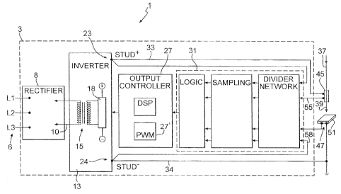
[0022] Referring now to the drawings wherein the showings are for purposes
of
illustrating embodiments of the invention only and not for purposes of
limiting the same,
FIGURE 1 shows a welder depicted generally at 1. The welder 1 includes a power
source
3 or power supply 3 shown in dashed lines. The power source 3 described
hereafter is
exemplary in nature. As such, persons of ordinary skill in the art will
readily understand
the application of the embodiments of the subject invention to welding power
supplies
including both DC and AC output power. The power source 3 is illustrative as a
high
switching speed inverter, such as the Power Wave manufactured by The Lincoln
Electric
Company in Cleveland, Ohio. In the current embodiment, three phase power 6,
shown by
input power lines Ll, L2 and L3, is directed to a power source rectifier 8
that produces a
DC signal through conductors 10, of which the DC signal may be further
directed to the
input of an inverter 13. The inverter 13 includes a transformer 15 having
primary and
secondary windings in a manner well known in the art. Output from the
secondary
windings may be directed to rectifier 18 providing positive and negative
supply power to
power output terminals 23, 24, respectively, also referred to as studs 23, 24.
The power
CA 02660631 2009-02-09
WO 2008/048726
PCT/US2007/072623
6
source 3 may further include a power output controller 27 electrically
communicated to
the rectifier 18 for gauging or controlling output power at the studs 23, 24
during the
welding process. In one embodiment, the controller 27 may include a pulse wave
modulator 27 or PWM 27'. Welding cables 33, 34 may be connected to the power
supply
3, and more specifically to the studs 23, 24, for delivering welding current
to a work piece
51 through an electrode 45 and work piece connector 47. Typically, the welding
cables
33, 34 are long having inherent impedance characteristics as mentioned above.
An
electrode 45 may include welding wire 37 supplied from a continuous source,
such as a
wire feeder, not shown, through contact tip 39 to which positive welding cable
33 is
electrically connected. Similarly, welding cable 34 may include a work piece
connector
47 for electrically connecting the welding cable 34 and the work piece 51.
[0023] With continued reference to Figure 1, the controller 27 may also
include a
wavefoim generator or other digital signal processor (DSP) 28 in accordance
with
standard welding technology. The controller 27 may be used to control the
power output
between the electrode 45 and the work piece connector 47. Welding is initiated
by
engaging the pulse width modulator 27' according to a command signal or output
enable
signal and a feedback signal via remote welding sense leads 55, 58. As such,
the
controller 27 may utilize the feedback signal to adjust power output at the
studs for
maintaining a high quality weld. The remote welding sense leads 55, 58 may be
electrically connected between the power source 3 and the electrode 45 and the
work
piece 51 respectively to direct feedback signals representative of the
operating parameters
at the welding site. In this manner, feedback signals from the sense leads 55,
58 may be
combined with the command signal in the digital signal processor 28 to adjust
the power
output as needed. Each of the remote welding sense leads 55, 58 may be
connected to
one of either of the electrode 45 or the work piece 47. More particularly, the
remote
welding sense leads 55, 58 may be interchangeably connected to the electrode
or the work
piece without configuring the power supply 3 and without adversely affecting
the power
output as managed by the controller 27. As will be described in detail below,
a feedback
conditioning circuit 31 may be incorporated to receive the signals generated
through the
sense leads 55, 58 and derive a feedback signal that may be used by the
controller 27 to
adjust the power output supply while compensating for any configuration of
sense lead
55, 58 connections including misconnected and broken or severed sense lead
wires.
CA 02660631 2011-03-02
7
Thus, the embodiments of the invention may relate to a feedback controller
that
automatically adjusts the feedback signal for any connection of sense leads
without
configuring the power supply 3.
[0024] In preparation for the welding process, the operator may connect the
sense leads
55, 58 at first ends to respective sense lead connectors located on the
welding supply and
at second ends respectively to the electrode 45 and the work piece 47. Prior
to the advent
of the embodiments of the subject invention, the operator had to configure the
power
supply according to the connection and type of the sense leads used. Prior art
power
sources may be configured, in one manner, by setting the order of a specific
set of
switches that signal the controller to process input from the sense leads in a
prescribed
manner. However, misconnection of those sense leads with respect to the switch
settings
resulted in poor weld quality and in certain circumstances irreparable damage
to the work
piece. In contrast, the embodiments of the present invention sense the
connection
configuration of the sense leads 55, 58 and automatically adjust the feedback
signal used
by the controller 27 responsive to the connection of the sense leads via the
feedback
conditioning circuit 31.
[0025] With continued reference to Figure 1, the feedback conditioning
circuit 31
may include a signal conditioning circuit, a sampling circuit 81 and logic
processor 99.
The signal conditioning circuit receives the signals generated through the
sense leads 55,
58, scales the input signals and segments the signals into separate signal
components
representing both magnitude and polarity. The signals may then be converted
into digital
signals by the sampling circuit 81. Thereafter, the digitally converted
signals are shifted
into a logic processor 99 that derives a feedback signal based upon the
magnitude of the
input signals and the polarity of the sense leads. Output from the processor
may
subsequently be communicated to the controller 27 for access to the
conditioned feedback
signal in combining it with the command signal to adjust the power signal
accordingly.
[0026] With reference now to Figure 2, the signal conditioning circuit 42 may
include
a voltage divider network 65. Input signals detected at the work piece 51 may
be directed
through the sense leads 55, 58 as previously mentioned, of which the input
signals may be
analog signals representing one or more electrical parameters of the welding
process. For
example, a first sense lead signal returned by sense lead 55 may represent the
operating
voltage at the electrode E. Similarly, a second sense lead signal may
represent the
CA 02660631 2009-02-09
WO 2008/048726
PCT/US2007/072623
8
operating voltage at the work piece W via sense lead 58. The input signals or
signals
from the sense leads 55, 58 may be directed to the voltage divider network 65,
which may
include a network of resistors or other resistive components including passive
and/or
active devices, for scaling the representative signals. For exemplary purposes
the voltage
divider network 65 will be described using resistor components 62. However,
any means
for scaling the input signals may be chosen with sound engineering judgment.
The
voltage divider network 65 may utilize multiple resistor components 62
connected in
series to form the voltage divider network 65. Nodes 68 may be defined as the
junction
between the resistor components 62. In one branch of the voltage divider
network 65,
two resistors R1 and R2 may be connected in series between one of the sense
leads and a
reference voltage VREFI. A parallel branch may similarly be connected between
the other
sense lead and the common reference voltage VREF1. It will be appreciated by
persons of
ordinary skill in the art that scaled input signals may be drawn from the
nodes 68 between
the resistors R1, R2 respectively. The degree of scaling will naturally depend
upon the
values of the resistors R1, R2 and the reference voltage VREF1. In one
embodiment, the
resistor value of R1 may be substantially 100 Kilo-Ohms and R2 may be
substantially 5
Kilo-Ohms. However, any ratio of resistance values for R1 and R2 may be chosen
as is
appropriate for scaling the input signals in accordance with the embodiments
of the
subject invention. It is noted here that each branch of the voltage divider
network 65 may
scale the signals in the same manner. In other words, the voltage divider
network 65 may
comprise one or more substantially identical branches with resistors 62 having
substantially the same values in the same order with respect to a common
reference
voltage V REFI. As such, similarly scaled input signal values will be present
at each of the
respective nodes 68, 68' of the parallel branches.
100271 With
reference now to Figures 2 and 3, the signal conditioning circuit 42 may
further comprise a plurality of parallel branch rectifying circuits 75 that
further condition
the intermediate feedback signals as taken from nodes 68, 68'. In one
embodiment, each
of the parallel branch circuits 75, as shown in dashed lines, may include a
rectifying
circuit 77 and an inverting rectifying 79 circuit. Input signals scaled by the
voltage
divider network 65 may be directed into each of the rectifying circuits 77, 79
for detecting
the magnitude and the polarity of the sense leads 55, 58. For example, a first
signal
directed from the electrode E may be scaled by the voltage divider network 65
and
CA 02660631 2009-02-09
WO 2008/048726
PCT/US2007/072623
9
subsequently directed into a rectifying circuit 77. The rectifying circuit 77
may be a half-
wave rectifier that amplifies only positive components of the signal. In a
parallel branch,
inverting circuit 79 inverts the signal and rectifies the inverted signal.
Similarly, a second
input signal directed from the work piece W may be conditioned by a parallel
set of
inverting and rectifying circuits also segmenting the second input signal into
separate
components. Therefore the rectifying circuits 77, 79 breakdown the inputs
signals
received by the sense leads 55, 58 for processing by a logic processor and/or
other
circuitry to determine the polarity connection of the sense leads 55, 58.
100281 With reference now to Figures 4 and 5, in one embodiment the input
signals
may be rectified and inverted using precision rectifiers. Precision rectifiers
may be
implemented using an op-amp 61 (operational amplifier) and may include one or
more
diodes 63 in the feedback loop. This effectively cancels the forward voltage
drop of the
diode allowing low level signals to still be rectified with minimal error.
Figure 4 depicts
one configuration of precision rectifier where the input signal is both
rectified and
inverted. In this embodiment, the precision rectifier may be a half wave
rectifier where
the input signal values are inverted. The negative values, up to a particular
level, are
cropped. Figure 5 depicts another configuration of precision rectifier that
crops negative
input signals values within a specific range but amplifies the positive
signals. The degree
of amplification may depend on the values of the resistor elements R3 through
R8, which
may be any chosen value as is appropriate for amplifying the intettnediate
signals
according to the embodiments of the subject invention. For example, R3 and R4
may be
100 Kilo-ohms. R5 and R7 may be approximately 100 Ohms. R6 and R8 may be 1.5
Kilo-Ohms. It should be noted that these resistance values are exemplary in
nature. As
such, any resistor values may be chosen with sound engineering judgment. The
rectifying
77 and inverting 79 circuits may be connected in parallel as shown in Figure
3. This
functions to segment the input signals, the use of which will be discussed
further with the
continued description of the embodiments of the subject invention.
[00291 With reference again to Figures 1 and 2, the input signals, as
detected by the
sense leads 55, 58, may be analog signals. The analog input signals are scaled
by the
voltage divider network 65 and segmented by the rectifying circuits 75.
Accordingly,
signals output from the signal conditioning circuit 42 may also be analog
signals. The
intettnediate analog signals may subsequently be directed into sampling
circuits 81 as
CA 02660631 2009-02-09
WO 2008/048726
PCT/US2007/072623
shown in Figure 2 by dashed lines. The sampling circuits 81 may convert the
intermediate analog signals into digital signals for subsequent processing by
a digital
logic processor as will be discussed further in subsequent paragraphs. In one
embodiment, the sampling circuit 81 may comprise analog-to-digital converters
91, or
A/D converters 91, that sample, hold and convert the intemiediate analog
signals thereby
translating the analog signal values into binary numbers. One example of an
A/D
converter is the ADS7886 manufactured by Texas Instruments, which samples at a
rate of
up to 1 MSPS (Mega-Samples-Per-Second). The ADS7886 may convert the analog
signal into a 12-bit binary number. The feedback conditioning circuit 31 may
include one
A/D converter 91 for each segmented intermediate analog signal. As such, each
of the
segmented values may be digitally converted at substantially the same time. In
other
words, each of the rectifying and inverting circuits may be electrically
communicated to
individual corresponding A/D converters 91 thus comprising a plurality
parallel branch
circuits for simultaneous operation. While the aforementioned sampling circuit
81 is
described utilizing a particular commercially available model, it is to be
understood that
any model of A/D converter or any other circuitry converting analog signals
into digital
signals may be used without departing from the scope of the embodiments of the
subject
invention. In other words, any manner of digitally converting the intermediate
analog
signals may be chosen with sound engineering judgment. Data communication from
the
A/D converters 91 to the logic processor 99 may be synchronized by a clock
signal
common to all of the components 91, 99. In one embodiment, the logic processor
99 may
include multiple data inputs for receiving data at each of the input channels
during the
same clock cycle. Thus, conditioned feedback data from the sense leads 55, 58
are
received by the logic processor 99 in a synchronized and substantially
simultaneous
manner.
10030] With reference again to Figures 1 and 2 and now also to Figures 6,
logic
devices or logic processors 99 can be classified into two broad categories:
fixed and
programmable. Naturally, the circuits in a fixed logic device cannot be
changed. On the
other hand, programmable logic processors can be changed at any time to
perfoun any
number of functions. In one embodiment of the subject invention, the logic
processor 99
may comprise a programmable logic processor 99, such as a field-programmable
gate
array 99' frequently referred to as an FPGA. FPGAs are similar in principle
to, but have
CA 02660631 2009-02-09
WO 2008/048726
PCT/US2007/072623
11
wider potential application than, programmable read-only memory integrated
circuits. An
FPGA is a semiconductor device containing programmable logic components and
programmable interconnects that can be programmed to duplicate the
functionality of
basic logic gates (e.g. AND, OR, XOR, NOT) or even more complex arithmetic
functions. The logic processor 99 may combine one or more binary inputs as
received
from the A/D converters 91 to one or more outputs according to a Boolean logic
function
in a predetermined manner. Specifically, the processor's logic may be
physically
implemented as a small look-up table memory, as shown in Figure 7. However,
the
processor's logic may alternatively be implemented as a set of multiplexers
and/or gates.
It is noted here that while the logic processor 99 is exemplified as an FPGA,
it is to be
construed that any type of logic devices, either fixed and/or programmable,
may be
chosen with sound engineering judgment for implementing the logic functions as
described herein without departing from the intended scope of the embodiments
of the
subject invention.
10031] With reference again to Figure 6, similar to the circuits for
conditioning the
input signals from the sense leads 55, 58, the feedback conditioning circuit
31 may further
include additional circuits for scaling and amplifying signals representing
the operating
parameters, and more specifically voltage, at the studs 23, 24. These
circuits, as shown in
Figure 6, are directed through a voltage divider network 65', rectifying
circuits 77' and are
digitally converted by corresponding A./D converters 91'. The signals are
subsequently
shifted into the logic processor 99 in a synchronous manner along with the
conditioned
signals from the sense leads 55, 58. As such, DIN 2 receives data
representative of the
scaled signal from the positive stud 23 and DIN 3 receives the scaled signal
from the
negative stud 24. It is noted that the signals from the studs 23, 24 may not
be segmented
as are the signals from the sense leads 55, 58. That is to say that the
signals from the
studs 23, 24 may be rectified and/or amplified but may not inverted. Each of
these
signals may be used in conjunction with the signals from the sense leads 55,
58 to derive
an output feedback signal as deteimined by the logic table shown in Figure 7.
100321 With reference now to Figures 4 through 6, as mentioned above input
signals
from the sense leads 55, 58 may represent one or more operating parameters,
and more
specifically voltage, of the welding process at the weld site. Each sense lead
returns an
input signal that may be segmented and used to determine the polarity of the
sense leads
CA 02660631 2009-02-09
WO 2008/048726
PCT/US2007/072623
12
55, 58 and to derive a feedback signal for correcting the power output at the
studs 23, 24.
Each of the input signals, one representing the electrode E and the other
representing the
work piece W, may be scaled via the voltage divider network 65 and
subsequently
directed into parallel precision rectifier circuits that separately rectify
and invert the
signals thereby deriving at least two separate components of each input
signal. The
outputs of the rectifying circuits and subsequent digitally converted
equivalent may be
directed into the logic processor 99, which may perfolin logic functions on
the data
thereby deriving the feedback values. It will be readily seen from Figure 6
that the input
DIN 0 of the logic processor 99 corresponds to the inverted signal from the
electrode E.
Similarly, DIN 1 corresponds to the rectified signal of the electrode E.
Likewise, DIN 4
and 5 correspond to the inverted and rectified signals from the work piece
respectively.
The logic table, as depicted in Figure 7, shows one relationship for logically
processing
the input data. Accordingly, the logic processor 99 may calculate an output
feedback
signal responsive to the values of the conditioned input signals as received
by the input
channels DIN 0 through DIN 5.
[0033] With reference to Figures 6 and 7, the signal data received by the
digital inputs
of the logic processor 99 may be used to populate the logic inputs of the
logic table. In
one embodiment, the digital input values may be compared to base value or
threshold
value to determine the connectivity of the sense leads and correspondingly to
determine
which signal parameters will be used to calculate the feedback signal.
Accordingly, for
input signals below the threshold value, a zero (0) will be placed in the
logic table under
the column for the particular input, e.g. DINO, DIN1. Similarly, for input
signal values
above the threshold value, a one (1) will be placed in the corresponding
column. It is
noted that the magnitude of the actual signal values are not changed by
comparison to the
threshold value. Rather the derived data may be stored internally, or
externally, in
memory for access by the processor in calculating the feedback signal. It
should be noted
that since the input signal values may be scaled by the voltage divider
network 65, 65', a
threshold value may be chosen to coincide with the conditioned input signals
values.
However, any threshold value may be chosen as is appropriate for use with the
embodiments of the subject invention. For example, if the signal at the
electrode E is
positive, DIN 1 will receive a scaled value proportionate to the magnitude of
the signal at
the electrode and DIN 0 will have a value of substantially zero. Additionally,
if the signal
CA 02660631 2009-02-09
WO 2008/048726
PCT/US2007/072623
13
at the work piece W is zero, accordingly DIN 4 and DIN 5 will also be
substantially zero.
The logic processor 99 may compare the values of the logic processor input,
i.e. DIN 0 ¨
DIN 5, with respect to the threshold value. The logic inputs may be populated
and the
logic table then examined to determine which logic function will be used to
derive a
feedback signal. In the instance where the positive value of DIN 1 meets or
exceeds the
threshold value, the logic processor 99 may assign a value of one (1) to the
logic input
corresponding to that digital input of the logic table. The logic processor 99
may
therefore calculate the feedback signal value as the difference between the
value of DIN1
and DIN3 as prescribed by the logic table. In the instance where the value of
the signal
received at DIN1 is positive but less than the threshold value, a value of
zero (0) will be
assigned to the logic table in the DIN1 column. In this instance, the logic
processor 99
may calculate the feedback signal value based on the difference between the
values of
DIN2 and DIN3. Once the value of the feedback signal has been calculated, it
may be
stored in a memory unit of the logic processor 99. In one embodiment, the
logic
processor 99 may be an FPGA 99' and the memory unit may be an internal
register
accessible by the controller 27. However, any manner of storing and
communicating the
calculated value of the feedback signal may be chosen with sound engineering
judgment.
[0034] With reference now to Figures 8.1 and Figure 9, another example of
the
operation of the feedback conditioning circuit 31 will now be described.
Welding power
output at the studs 23, 24 may range between a positive maximum magnitude and
a
negative maximum magnitude respectively. Figure 8.1 shows sense lead 58
connected to
the work piece and sense lead 55 connected to the electrode 45. The sense
leads 55, 58
may direct input signals through terminals E, W of the feedback conditioning
circuit 31
respectively. It will be recognized that DINO and DIN1 represent signals
generated by
sense lead 55 and similarly DIN4 and DIN5 represent signals from sense lead
58. A
positive signal value at the electrode E may result in DINO equaling
substantially zero (0)
and DIN1 equaling a value proportional to the electrode E signal magnitude
above the
threshold value. Additionally, DFN4 may receive a positive value proportional
to the
work piece W signal magnitude above the threshold value and DIN5 may be
substantially
zero (0). Based on the logic table value, the feedback signal will be based on
the
difference between DINO and D1N4, which will be readily seen as the scaled
values
returned by the sense leads 55, 58.
CA 02660631 2009-02-09
WO 2008/048726
PCT/US2007/072623
14
[0035] With continued reference to Figure 8.1 and Figure 9, the above
described
example may represent one operating condition of the welder 1 where the sense
leads 55,
58 are correctly connected to the power supply 3. However, in the event that
one of the
sense leads 55, 58 becomes disconnected, the feedback conditioning circuit 31
may
automatically adjust for the disconnection. If this example, sense lead 55 may
become
disconnected from communicating an input signal into the feedback conditioning
circuit
31. The signal received at the corresponding logic processor inputs DINO, DIN1
may be
substantially zero and thus the logic table for DINO and DIN1 will
correspondingly be
zero (0). The feedback conditioning circuit 31 may quickly compensate for the
disconnected lead by adjusting the logic function used to calculate the
feedback signal.
Specifically, the feedback value will now be based on the difference between
D1N2 and
DIN4, which relates to the scaled values of the positive stud 23 and the
inverted sense
lead 58. It is noted that the feedback conditioning circuit 31 quickly adjusts
for the
disconnection via the logic processor. The aforementioned example points out
the
robustness of the feedback conditioning circuit 31. That is to say that the
feedback
conditioning circuit 31 may quickly respond to changes in the welder 1. This
may be
attributed to the substantially simultaneous conditioning of the input signals
and
synchronized shifting of data into the logic processor 99.
[0036] With reference now to Figure 8.2, the operator of the welder 1 may
switch the
connection of the sense leads 55, 58, with respect to the configuration shown
in Figure
8.1, without having to configure the power supply 3 and without experiencing
adverse
affects on the welding process. For this configuration of sense lead
connections, the input
signal values E, W may be inverted respectively. Accordingly, logic table
values for
DINO may be one (1) and DIN1 may be zero (0). Additionally, logic table values
for
DIN4 may be zero (0) and DINS may be one (1). The feedback signal will
therefore be
based on the difference between actual values received at DIN5 and DINO. Thus,
the
juxtaposition of the sense leads between the electrode and the work piece may
result in an
automatic adjustment of the feedback signal.
[0037] The logic processor 99, once it has completed the calculation of the
feedback
signal, may store the value in an internal register as previously mentioned.
The controller
27 may be electrically communicated to the logic processor 99 for access to
the register.
The command signal may therefore be adjusted by combining a previously
computed
CA 02660631 2009-02-09
WO 2008/048726
PCT/US2007/072623
command signal with the new feedback signal as retrieved from the logic
processor 99,
[0038] The invention has been described herein with reference to the
preferred
embodiment. Obviously, modifications and alterations will occur to others upon
a reading
and understanding of this specification. It is intended to include all such
modifications
and alternations in so far as they come within the scope of the appended
claims or the
equivalence thereof.