Note: Descriptions are shown in the official language in which they were submitted.
CA 02660706 2009-02-12
1
DESCRIPTION
ROOM-TEMPERATURE BONDING METHOD AND ROOM-TEMPERATURE
BONDING APPARATUS
Technical Field
The present invention relates to a room-temperature
bonding method and a room-temperature bonding apparatus.
The present invention particularly relates to
room-temperature bonding of substrates using an
intermediate member.
Background Art
Basic technical contents of a room-temperature
bonding method based on a surface activation method are
disclosed in Japanese Laid-Open Patent Application
JP-A-Showa 62-22712 (Japanese Patent JP1422397B) and
Japanese Patent JP2791429B. However, since there are some
materials difficult to bond together at a room temperature
even by using this method, a bonding method in such a case
is disclosed in following documents.
For example, after ion beams or atom beams using Ar
or the like are irradiated onto surfaces to be bonded not
only for removing contamination layers on the surfaces to
be bonded but also for activating the surfaces to be bonded,
an active ultrafine particle film is further formed on each
of the surfaces to be bonded. At this time, as a method
of forming an active layer, a target material is sputtered
CA 02660706 2009-02-12
2
to thereby form the active ultrafine particle film on the
surface to be bonded, opposed to the target. However, it
is described that because of a low density of the ultrafine
particle film, it is preferable to heat the surfaces so
as to improve a degree of sintering during bonding (Japanese
Laid-Open Patent Application JP-A-Heisei 6-99317).
Furthermore, varioustypesofinetalfilmseach having
good adhesiveness can be formed on diverse materials by
using active Ti, Cr or the like as an intermediate layer.
By using this intermediate layer to form a metal film on
a surface of a material such as Si02 for which sufficient
adhesion strength cannot be obtainedby direct bonding based
on the surface activation method, it is expected to be able
to improve a performance of bonding of the material. Si,
SiO2 and LiNbO3 are disclosed as examples of the material,
and Pt as well as Ti and Cr is disclosed as an example of
a material of the intermediate layer (Report of Mechanical
Engineering Laboratory, No. 189, Chapter 8, December,
2000).
It is disclosed that irradiating inert gas ion beams
or inert gas neutral atomic beams and metal ion beams or
metal neutral atomic beams onto surfaces to be bonded of
two substrates in vacuum to thereby form a metal thin film
having a film thickness of 1 nm to 100 nm on each of the
surfaces to be bonded of the substrates so as to bond, at
a low temperature, the substrates having surfaces composed
of ionic crystals and difficult to bond together by the
CA 02660706 2009-02-12
3
conventional surface activation method. Fig. 6 shows an
example of the irradiation. A Si02 substrate 107 is used
as the siubstrate to be bonded, iron atoms 106 are used for
the metal neutral atomic beam and argon atoms 105 are used
for the inert gas neutral atomic beam. Each of the beams
is irradiated from a beam irradiation unit 102 that includes
therein an electrode 101, a beam source 103 and a grid 104.
Specifically, the iron atoms 106 are generated as follows.
The grid 104 composed of iron is disposed in an opening
portion of the beam source 103, a part of argon atomic beams
generated by applying a voltage to the electrode 101 from
the beam source 103 strikes against the grid 104, and a
part of the struck grid 104 is sputtered. Quartz, silicon
oxide, silicon nitride, sapphire and LiNbO3 are disclosed
as examples of the ionic crystal, and iron, titanium and
gold are disclosed as examples of a type of the metal. If
the grid is replaced by another grid, the type of the metal
can be changed. This method is characterized in that
surface activation of the surface to be bonded of the
substrate and deposition of a metal thin film are
simultaneously performed. Therefore, by adjusting energy
of either the ion beams or the neutral atomic beams, it
is controlled to preferentially perform an action of
activation or an action of metal thin film deposition.
However, to improve a bonding strength, it is necessary
to heat each substrate to 150 C to 500 C and to press
the substrates by a roller during bonding. It is also
CA 02660706 2009-02-12
4
necessary to produce another grid so as to change the type
of the metal thin film. It is, therefore, not easy to change
the type of the metal thin film (Japanese Laid-Open Patent
Application JP2004-337927A).
Amethod of accelerating bonding is disclosed in which
a metal thin film layer or an amorphous layer is formed
on a bonding interface. This method is to bond a
polycrystalline substance to a single-crystalline
substance where it is difficult for both of the crystalline
substances to realize a smooth surface roughness. The
metal thin film layer is formed on a surface to be bonded
of the polycrystalline substance, and the amorphous layer
containing an elementconstitutingthesingle--crystalline
substance or an element of a metal constituting the metal
thin film layer is formed on a surface to be bonded of the
single-crystalline substance. Thereafter, the surfaces
are activated and bonded to each other. Sintered ceramic
isdisclosed as the polycrystalline substance, andSi, SiGe
and GaAs are disclosed as the single-crystal line substance.
Pt (platinum) and Au (gold) are disclosed as the metal.
As a method of forming the metal thin film, a sputtering
film formation method is disclosed which uses an ion beam
obtained by irradiating plasma ions onto a target and using
recoil particles as f ilm formation particles. This method
is a method of bonding the substances by the amorphous layer
produced by a reaction between the metal and the
semiconductor, and application of the method is limited
CA 02660706 2009-02-12
to semiconductor substrate materials (Japanese Laid-Open
Patent Application JP2005-104810A).
Disclosure of Invention
5 As stated above, there is known the technique for
improving the bonding strength by interposing another
material between the surfaces to be bonded so as to bond
two substrates that are difficult to bond by
room-temperature bonding. However, if the
room-temperature bonding is to be actually performed on
substrates with the intermediate layer interposed between
the substrates, there is a problem that a sufficient bonding
strength cannot be obtained unless the conventionally used
technique, such as heating and/or pressing of the substrates
during bonding, is adopted since the bonding strength is
insufficient at a room temperature. Furthermore, the
sputtering by ion beams is used as the technique for forming
the intermediate layer. However, a specific method and
a specific apparatus configuration for uniformly forming
the intermediate layer over entire surfaces of the
substrates are not disclosed. Therefore, a
room-temperature bonding method and a room-temperature
bonding apparatus for ensuring a uniform bonding strength
over the entire surfaces of the substrates are not disclosed.
Moreover, a method of appropriately controlling
composition of an intermediate member when bonding
substrates with the intermediate member containing a
CA 02660706 2009-02-12
6
plurality of types of metals interposed therebetween is
not disclosed.
An object of the present invention is to provide a
method and apparatus for uniformly forming an intermediate
member on a surface of a substrate and obtaining a sufficient
bonding strength even by room-temperature bonding without
heating the substrates during bonding. Specifically, an
object of the present invention is to provide a
room-temperature bonding method and room-temperature
bonding apparatus when an intermediate member is composed
of a plurality of types of materials.
The present invention relates to a method and
apparatusforroom- temperaturebondingsubstratestogether
using an intermediate member. By radiating ion beams or
atom beams onto a target/targets composed of a plurality
of types of materials and simultaneously sputtering the
materials, the intermediate member is formed. The
target/targets mentioned in the present invention
refers/referto materials of the intermediate member formed
on a surface to be bonded of a substrate by sputtering.
A first aspect of the present invention is a method
of room-temperature bonding a plurality of substrates via
an intermediate member, including steps of: forming the
intermediate member on a surface to be bonded of the
substrate by physically sputtering apluralityof targets;
and activating the surface to be bonded by ion beams. In
this case, it is preferable that the target/targets composed
CA 02660706 2009-02-12
7
of a plurality of types of materials is/are physically
sputtered. Sincethe materialsof theintermediate member
are sputtered from the plurality of targets arranged in
various directions from the surface to be bonded of the
substrate, the intermediatemembercan be uniformly formed
on the surface to be bonded. Further, since the
intermediate member is composed of the plurality of types
of materials, the room-temperature bonding of substrates
difficult to bond together when an intermediate member is
composed of a single type of material can be performed
without heating and excessively pressing the substrates
during bonding. Examples of the substrates include a
silicon substrate and a SiO= substrate. Examples of the
materials include metal and dielectric. Examples of the
physical sputtering include sputtering by irradiation of
an ion beam, sputtering by irradiation of a neutral particle
beam (Fast Atom Beam, hereinafter referred to as "FAB"),
sputtering by irradiation of plasma and sputtering by
irradiation of a laser beam. When the beam is positively
charged, electrons may be irradiated onto the beam from
an electron gun to neutralize the beam so as to avoid
charge-up on the surface to be bonded of each substrate.
Further, the step of forming the intermediate member and
the activation step may be executed in an arbitrary order.
The activation may be performed after forming the
intermediate member, the formation of the intermediate
member and the activation maybe performed simultaneously,
CA 02660706 2009-02-12
8
or the intermediate member may be formed after the
activation. Moreover, steps of a combination of these may
be executed. For example, after performing only the
activation, the activation and the formation of the
intermediate member may be simultaneously performed. The
order of the steps should be appropriately changed since
a surface state of the surface to be bonded after forming
the intermediate member and a surface state of the surface
to be bonded after the activation depend on materials of
the substrates and the intermediate member and conditions
for sputtering and activation. Due to this, priorities
of the steps cannot be uniformly decided. Namely, the order
is decided depending on bonding conditions. However, it
is more preferable to simultaneously perform the formation
of the intermediate member and the activation since the
number of steps can be reduced.
Moreover, by using an alloy as the target, a plurality
of types of metals can be easily sputtered. By setting
a composition ratio of the alloy to be equal to a desired
composition ratio of the intermediate member, the
intermediate member can be controlled to have a desired
composition. As a result, by changing the composition
ratio of the alloy based on the type of the substrate, a
desired substrate bonding strength can be obtained.
Nevertheless, a sputtering efficiency often differs
depending on the type of inetal of the target . In that case,
if the composition ratio of the alloy is decided also in
CA 02660706 2009-02-12
9
view of the efficiency, an intermediate member having a
desired composition can be obtained.
Further, when a plurality of types of materials is
arranged to be independent of one another as the target
and the target is sputtered, it is possible to
simultaneously sputter the plurality of types of materials.
If it is difficult to produce an alloy composed of the
plurality of types of metals, the intermediate member
composed of the plurality of types of metals can be formed
by independently arranging the metals and simultaneously
sputtering the metals.
Furthermore, when an area ratio of surfaces of the,
plurality of types of materials to be irradiated with ion
beams or atom beams is set based on the desired composition
ratio of the intermediate member, the intermediate member
can be controlled to have desired composition. Asaresult,
by changing the composition ratio of the alloy based on
the type of the substrates or changing the area ratio of
the surfaces to be irradiated based on the plurality of
types of materials, the intermediate member can be
controlled to have a desired composition. Therefore, a
desired substrate bonding strength can be obtained. In
this case, similarly to the above-stated case, the
sputtering efficiency often differs depending on the type
of metal of the target. In that case, if the composition
ratio of the alloy and the area ratio of the surfaces to
be irradiated based on the materials are decided also in
CA 02660706 2009-02-12
view of the efficiency, the intermediate member having the
desired composition can be obtained.
A second aspect of the present invention is a
room-temperature bonding apparatus including: a vacuum
5 chamber; an evacuation apparatus evacuating the vacuum
chamber; a pair of substrate holders arranged to face each
other in the vacuum chamber; a pressure bonding mechanism
connectedtothesubstrateholdertobondsubstratesmounted
on the respective substrate holders to each other; and a
10 physical sputtering source, wherein a target irradiated
with ion beams or atom beams emitted from the physical
sputtering source is arranged in the vacuum chamber
independently of the substrate holders, the pressure
bonding mechanism and the physical sputtering source.
By arranging the target in the vacuum chamber
independently of the other devices and the like, an
intermediate member composed of a desired material with
a desired composition ratio can be formed on a surface to
be bonded of each substrate. Namely, it is possible to
suppress the intermediate member from being composed of
arbitrary metals possibly sputtered from the other devices
or the like. Therefore, adhesion of the metal unnecessary
for the intermediate member onto the surface to be bonded
of each substrate can be suppressed, and the intermediate
member suitable for a material of the substrates to be bonded
can be selectively formed. As a result, the substrates
that are conventionally difficult to bond together by
CA 02660706 2009-02-12
11
room-temperature bonding can be bonded to each other at
a desired bonding strength. Examples of the physical
sputtering source include an ion beam source, an FAB source,
a plasma source and a laser source. Examples of the energy
beam include an ion beam, a neutral atomic beam, a beam
of ions or neutral particles in plasma and a laser beam.
Furthermore, by mounting the target on a target
substrate, the target necessary for bonding can be easily
arranged in the vacuum chamber. This can facilitate fixing
the target into the vacuum chamber. Besides, when a
plurality of types of materials is used as the target and
the materials are arranged independently of one another,
then the materials are temporarily mounted on the target
substrate and the target substrate is arranged in the vacuum
chamber. This can facilitate handling such as replacement
of the target as compared with arranging targets
independently in the vacuum chamber. The target substrate
mentioned in the present invention refers to a substrate
for holding the target and is not a material composed of
the intermediate member.
As a method of mounting the target on the target
substrate, a bulk target such as a plate target may be
attached onto the target substrate using a tool, a foil
target may be bonded onto the target substrate, or a target
film may be formed on the target substrate by PVD, CVD or
plating.
Further, the target is composed of a plurality of types
CA 02660706 2009-02-12
12
of metals and the plurality of types of inetals is arranged
to be independent of one another at a ratio based on the
composition ratio of the intermediate member or arranged
as an alloy having the ratio. By configuring the target
to arrange the plurality of types of metals independently
and sputtering the target, it is possible to simultaneously
sputter the plurality of types of metals. When it is
difficult to produce an alloy composed of the plurality
of types of metals, the intermediate member composed of
the plurality of types of metals can be formed by
independently arranging the metals and simultaneously
sputtering the metals. Furthermore, when an area ratio
of surfaces of the plurality of types of materials to be
irradiated with ion beams or atom beams is set based on
the desired composition ratio of the intermediate member,
the intermediate member can be controlled to have desired
composition. As a result, by changing the composition
ratio of the alloy based on the type of the substrates or
changing the area ratio of the irradiated surfaces of the
pluralityoftypesofmaterials,adesiredsubstratebonding
strength can be obtained. However, sputtering efficiency
often differs depending on the types of materials of the
target. In that case, when the composition ratio of the
alloy and the area ratio of the irradiated surfaces of the
plurality of materials are decided also in view of the
efficiency, the intermediate member having the desired
composition can be obtained.
CA 02660706 2009-02-12
13
Moreover, by composing the target by an alloy, the
plurality of types of metals can be easily sputtered. By
setting the composition ratio of the alloy based on the
desired composition ratio of the intermediate member, the
intermediate member can be controlled to have a desired
composition. As a result, by changing the composition
ratio of the alloy based on the type of the substrates,
a desired substrate bonding strength can be obtained. In
this case similarly to the above, the sputtering efficiency
often differs depending on the types of inetals of the target.
In that case, when the composition ratio of the alloy is
decided also in view of the efficiency, the intermediate
member having a desired composition can be obtained.
Further, the surfaces to be irradiated of the target
are arranged so that the number of the surfaces is plural
so as to surround almost half a circumference of the
substrate and are oriented in a perpendicular direction
to the surface to be bonded of the substrate. To surround
almost half the circumference of the substrate means that
almost half the circumference is opened so as to prevent
targets from cutting off ion beams or atom beams emitted
from the physical sputtering source to the surfaces to be
irradiated, and means that the surfaces to be irradiated
can be appropriately arranged in a circumferential
direction so as not to cut off the ion beams or atom beams.
By arranging the targets to sandwich the surface to be bonded
of the substrate from the circumferential direction, metals
CA 02660706 2009-02-12
14
can enter a part of the surface to be bonded of the substrate
farther from the targets and the intermediate member can
be formedmore uniformly on the surface to be bonded thereof.
Furthermore, a shape of the surface to be irradiated
of the target is curved so that when the ion beams or atom
beams emitted from the physical sputtering source to the
surface to be irradiated generate sputtered atoms on
respective portions of the target in directions of regular
reflection, thesputteredatomsareparalleltooneanother
toward a position of the surface to be bonded of the substrate.
For example, the ion beams emitted from an ion beam source
are emitted while being diffused. Due to this, if the ion
beams reach the target at the same angles as those of the
ion beams are diffused, each sputtered metal is emitted
non-uniformly around an outgoing angle direction decided
based on an incident angle of the beam. As a result, since
the metals reaching the surface to be bonded of the substrate
have a non-uniformly distribution and a thickness of the
formed intermediate member has a non-uniformly
distribution in a surface direction of the substrate.
Therefore, when the shape of the surface to be irradiated
of the target is curved so that the sputtered atoms are
parallel with respect to the ion beams or atom beams while
being diffused, the distribution of the thickness of the
intermediate member in the surface direction of the
substrate can be more uniformed. The incident rays refer
to the ion beams or atom beams directed to the targets,
CA 02660706 2009-02-12
and the outgoing rays refer to the sputtered atoms generated
from the targets by the incident rays.
Further, the target substrate includes a mechanism
for adjusting a distance between the surface to be
5 irradiated of the target and the surface to be bonded of
the substrate. By adjusting the distance between the
surface to be irradiated of the target and the surface to
be bonded of the substrate, amounts of metals sputtered
from the targets can be adjusted and metal concentrations
10 of the intermediate member formed on the surface to be bonded
of the substrate can be set uniform in the surface. Besides,
when the target or the target substrate physically disturbs
carrying the substrate in and out from the substrate holders,
a position of the target or the target substrate is moved
15 to avoid the disturbance. Then, the substrate is disposed
on the substrate holder. After that, the target or the
target substrate is returned to a predetermined position
and room-temperature bonding can be performed.
Brief Description of the Drawings
Fig. 1 is a cross-sectional front view of a
room-temperature bonding apparatus according to the
present invention;
Fig. 2 is a perspective view showing an example of
a method of forming intermediate members on substrates by
sputtering targets according to a first embodiment of the
present invention;
CA 02660706 2009-02-12
Fig. 3A is a top view showing an example of arranging
a plurality of types of targets on a target substrate
according to a second embodiment of the present invention;
Fig. 3B is a top view showing an example of arranging
a plurality of types of targets on a target substrate
accordingto the second embodiment of thepresent invention;
Fig. 4A is a perspective view showing a method of
forming intermediate members on substrates by sputtering
targets according to a third embodiment of the present
invention;
Fig. 4B is a side view showing the method of forming
the intermediate members on the substrates by sputtering
the target according to the third embodiment of the present
invention;
Fig. 4C is a top view showing the method of forming
the intermediate members on the substrates by sputtering
the targets according to the third embodiment of the present
invention;
Fig. 5A is a perspective view showing a method of
forming intermediate members on substrates by sputtering
targets according to a fourth embodiment of the present
invention;
Fig. SB is a top view showing the method of forming
the intermediate members on the substrates by sputtering
the targets according to the fourth embodiment of the
present invention;
Fig. 6 is a cross-sectional view showing a
CA 02660706 2009-02-12
17
conventional method of forming an intermediate member on
a substrate by sputtering a target;
Fig. 7A is a side view showing substrates bonded to
each other via an intermediate member;
Fig. 7B is a side view showing substrates bonded to
each other via an intermediate member;
Fig. 8A is a perspective view showing a method of
forming intermediate members on substrates by sputtering
targets according to a fifth embodiment of the present
invention;
Fig. 8B is a perspective view showing the method of
forming the intermediate members on the substrates by
sputtering the targets according to the fifth embodiment
of the present invention; and
Fig. 9 is a top view showing the method of forming
intermediate members on substrates by sputtering targets
according to the third and fourth embodiments of the present
invention.
Best Mode for Carrying out the Invention
Fig. 1 is a cross-sectional view of a room-temperature
bonding apparatus according to the present invention. A
vacuum chamber 1 is composed of stainless steel with a shape
of a rectangular parallelepiped. An evacuation apparatus
2 for evacuating air from the vacuum chamber is attached
to one of side surfaces of this vacuum chamber I. In Fig.
1, an evacuation port with a circular form is shown as a
partoftheevacuationapparatus2. Therefore, a direction
CA 02660706 2009-02-12
18
of evacuating air from the vacuum chamber by this evacuation
apparatus is a direction perpendicular to a paper surface.
The evacuation apparatus is a combination of a turbo
molecular pump and a rotary pump. A physical sputtering
source 6 is also attached to one of the side surfaces of
the vacuum chamber 1. The physical sputtering source 6
is attached to the side surface different from that to which
the evacuation apparatus 2 is attached. An emission port
16 from which energy beams are emitted from the physical
sputtering source 6 coincides with an opening provided in
the side surface of the vacuum chamber 1. Accordingly,
the energybeams such as ionbeams or atombeams are generated
in the physical sputtering source 6, pass through the
emission port 16, and enter the vacuum chamber 1. In Fig.
1, the ion beams or atom beams are emitted from a left side
toward a right side.
A pressure bonding mechanism 5, a mount 17 and
substrate holders 3a and 3b are incorporated into the vacuum
chamber 1. Each of the pressure bonding mechanism 5, the
mount 17 and the substrate holders 3a and 3b is composed
of stainless steel. A substrate 4 is mounted on the
substrate holder 3a without being fixed to the substrate
holder 3a, and the substrate holder 3b fixes the substrate
4 thereto by electrostatic chuck. The mount 17 is disposed
on a bottom surface of the vacuum chamber 1. The substrate
holder 3a is provided on the mount. A central position
of the mount 17 coincides with a central position of the
CA 02660706 2009-02-12
19
substrate holder 3a. Further, the pressure bonding
mechanism 5 is disposed to penetrate through an upper
surface of the vacuum chamber 1. A central position of
a lower surface of the pressure bonding mechanism 5
coincides with a central position of an upper surface of
the mount 17.
The substrate holder 3b is disposed on a lower surface
of the pressure bonding mechanism 5. The central position
of the bottom surface of the pressure bonding mechanism
5 coincides with a central position of the substrate holder
3b. The pressure bonding mechanism 5 is structured so that
the lower surface of the pressure bonding mechanism 5 is
movableinan axial directionof themechanism. A position
of the lower surface of the pressure bonding mechanism 5
on which the substrate holder 3b is disposed moves
vertically as indicated by an arrow 18. A moving distance
has a span of which the lower surface can be located downward
of an upper surface of the substrate holder 3a disposed
on the upper surface of the mount 17. The pressure bonding
mechanism 5 is structured to be able to apply a load to
the mount 17 when the lower surface of the pressure bonding
mechanism 5 contacts with the upper surfaces of the mount
17. Central axes of the substrate holders 3a and 3b coincide
with each other.
A target substrate Ba is disposed horizontally
sideways to the substrate holders 3a and a target substrate
8b is disposed horizontallysidewaystothesubstrateholder
CA 02660706 2009-02-12
3b. The target substrates 8a and 8b are composed of
stainless steel. Each of the target substrates 8a and 8b
has a moving mechanism that each target substrate 8a or
8b can move in a same direction as the arrow 18 indicating
5 the moving direction of the pressure bonding mechanism 5.
Each of the target substrates 8a and 8b has at least a
mechanism that can move each target 7 to a position where
an outgoing ray 9 from the physical sputtering source 6
does not cross a surface to be irradiated of each target
10 7. The reason why the components are composed of stainless
steel is as follows. By not using the other materials as
materials of the components, the components are prevented
from becoming supply sources of unnecessary materials for
the intermediate member.
15 Targets 7 are mounted on an upper surface of the target
substrate 8a and a lower surface of the target substrate
8b, respectively. Each of the targets 7 is an alloy composed
of a plurality of types of metals and is a bulk alloy with
a plate shape. The target 7 is fixed to one target substrate
20 8 by screws. These screws are also composed of, for example,
stainless steel so as not to become supply sources of the
unnecessary materials for the intermediate member.
Positions and directions of the target substrates Ba
and 8b are variable by mechanisms that are not shown. A
distance between 8a and 8b, a distance between the substrate
holders 3a and 3b, a direction of the physical sputtering
source 6 with respect to the opening and a direction of
CA 02660706 2009-02-12
21
the physical sputtering source 6 with respect to the
substrate 4 are variable. Since a mechanism that
directions of the ion beams or atom beams emitted from the
physical sputtering source 6 can be changed will be
complicated, the directions are almost set to fixed
directions. By changing the positions and directions of
the target substrate holders 8a and 8b, uniformity in a
thickness of the intermediate member formed on a substrate
surface in a direction of the substrate surface and
uniformity in a concentration of the material composing
the intermediate member are controlled.
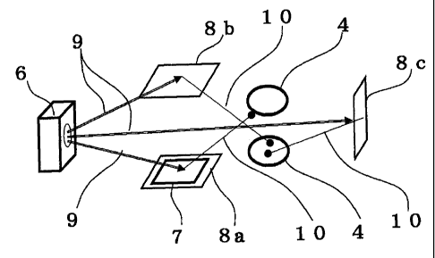
Fig. 2 is a perspective view of the room-temperature
bondingapparatus. In the case of Fig. 1, a target substrate
8c may be disposed. The ion beams or atom beams 9 emitted
from the physical sputtering source 6 are incident on
targets mounted on the target substrates 8a, 8b and 8c,
respectively. The metals composing the targets are
sputtered and the sputtered metals are emitted from the
targets to be sputtered atoms (sputter particles) 10 to
the substrates 4.
Figs. 1 and 2 do not show carrying in and out of the
substrates 3a and 3b. For example, a robot arm may be
provided in a load lock chamber disposed to communicate
with the vacuum chamber 1, the substrates 4 may be disposed
on the substrate holders 3a and 3b and the substrates 4
may be detached to be replaced by new substrates 4 after
being processed.
CA 02660706 2009-02-12
22
Procedures of room-temperature bonding using the
apparatus configured as stated above will be described.
Here, it is assumed that the target substrates 8a and 8b
and the targets 7 are disposed in advance. The substrates
4 to be bonded are transported into the vacuum chamber I
by means which is not shown and mounted on the upper surface
of the substrate holder 3a and on the lower surface of the
substrate holder 3b. The substrate 4 is mounted on the
substrate holder 3a without being fixed to the substrate
holder 3a, while the other substrate 4 is mounted on the
substrate holder 3b with being fixed to the substrate holder
3b byelectrostaticchuck. At this time, the lower surface
of the pressure bonding mechanism 5 is located at a higher
position than the upper surface of the mount in a direction
of gravitational force. After mounting the substrates,
the opening from which the substrates are carried in and
out of the vacuum chamber 1 is closed and evacuation of
the air from the vacuum chamber 1 is started by the evacuation
apparatus 2. After the vacuum chamber 1 reaches a
predetermined degree of vacuum, the physical sputtering
source 6 is actuated to emit, e. g. , ion beams 9. The ion
beams are incident on the targets 7 to emit elements composed
of the targets 7. In this case, since each target 7 is
composed of the alloy, a plurality of types of elements
composed of the alloy is emitted by sputtering. The
sputtered atoms 10, which are the plurality of types of
metal atoms sputtered and emitted, reach the substrates
CA 02660706 2009-02-12
23
4 and are deposited on surfaces of the substrates 4. At
the same time, the ion beams that are not incident on the
targets 7 are incident on the surfaces to be bonded of the
substrates 4. At this time, deposition of the metal atoms
and activation of the surfaces to be bonded by sputter
etching are simultaneously performed. A magnitude
relationship between action of the deposition and that of
the activation depends on arrangement of the targets 7,
magnitudes of the ion beams 9 from the physical sputtering
source 6 and an energy density distribution in a
perpendicular direction to the ion beams 9. Therefore,
the magnitude relationship between the action of the
deposition and that of the activation is adjusted by setting
them. Needless to say, such an adjustment that the action
of sputter etching exceeds the action of deposition is not
employed. The sputter etching means that a certain target
matter is sputtered by irradiating the certain target matter
with some energy beams and the irradiated portion is
eventually and physically ground.
After end of the deposition and the activation, the
physical sputtering source 6 is stopped to stop the emission
of the ion beams. Thereafter, the pressure bonding
mechanism 5 is driven to make the lower surface of the
pressure bonding mechanism 5 closer to the upper surface
of the mount 17. When the surfaces to be bonded of the
substrates 4 contact each other, a predetermined load is
applied to the pressure bonding mechanism 5 and the
CA 02660706 2009-02-12
24
application oftheloadiscontinuedforpredeterminedtime.
After passage of the predetermined time, the pressure
bonding mechanism 5 is drive in an opposite direction to
the moving direction to make the lower surface of the
pressurebonding mechanism5separatefromtheuppersurface
of the mount 17. At that moment, fixing of the substrate
4 to the substrate holder 3b is released. As a result,
the substrates 4 bonded to each other via the intermediate
member as shown in Figs. 7A and 7B remain on the substrate
holder 3a. Fig. 7A shows the intermediate member formed
in a layer shape and Fig. 7B shows the intermediate member
formed in a land shape. The bonded substrates 4 are carried
out to the load lock chamber by the robot arm and then pulled
out from the apparatus. New substrates are disposed in
the load lock chamber and subjected to room-temperature
bonding by the same method.
When the room-temperature bonding is performed as
stated above, a plurality of types of metals is mixed into
the surfaces to be bonded of the substrates as the materials
of the intermediate member to form the intermediate member
uniformly. Therefore, it is unnecessary to heat and
excessively press the substrates as conventionally
required in the bonding method, thereby making it possible
tonotonlysimplifytheroom- temperaturebondingapparatus
but also bond the substrates that are difficult to bond.
A first embodiment according to the present invention
will be described referring to Fig. 2. The reference
CA 02660706 2009-02-12
letters same as those shown in the other drawings denote
the same elements, respectively. In this embodiment, the
target substrate 8c is added to the configuration of the
apparatus shown in Fig. 1 and the others of the configuration
5 are the same as those shown in Fig. 1. The target substrate
8c has a same structure as that of the target substrates
8a and 8b. The target substrate 8c is disposed in a
direction perpendicular to the target substrates 8a and
8b on an opposite side to the target substrates 8a and 8b
10 with respect to the substrates 4 if viewed from the physical
sputtering source 6. The direction in which the target
substrate 8c is disposed also corresponds to a direction
in which the surface of the target substrate 8c is set
parallel to the opening 16 of the physical sputtering source
15 6. It is noted that the target substrate 8c is integrally
arranged on an extension of the surface direction of the
two substrates 4. Each target is plate-shaped and an alloy
of iron, chromium and nickel. Alternatively, the alloy
may be an alloy of metals selected from gold (Au) , aluminum
20 (Al), platinum (Pt), molybdenum (Mo), tungsten (W),
titanium (Ti) , tantalum (Ta) , iridium (Ir) , palladium (Pd)
silver (Ag), copper (Cu), cobalt (Co), rhodium (Rh),
ruthenium (Ru) and the like. As a method of mounting these
elements on the target substrate 8, it suffices to fix the
25 target ? so as not to move on the target substrate 8 using
a method of mounting a bulk alloy on the target substrate
8 and fixing it by screws or hooks. As the other fixing
CA 02660706 2009-02-12
26
methods, a method of fixing by adhesive or soldering, a
method of bonding by room-temperature bonding, a method
of attraction by electrostatic chuck or the like may be
used. The vacuum chamber 1 and the substrate holders 3a
and 3b may be composed of aluminum. The material of the
target substrates 8a, 8b and 8c may be composed of glass.
By employing the room-temperature bonding apparatus
arranged as stated above, a plurality of types of atoms
composed of the target 7 mounted on the substrate 8c is
sputtered from the target 7 by the ion beams 9 to the target
substrate 8c. The metal atoms emitted as the sputtered
atoms 10 reach the substrate 4 and are deposited on the
substrate 4, and the intermediate member can be formed.
In this case, for formation of the intermediate member on
the surface of the substrate 4 at a farther position from
the physical sputtering source 6 with the target substrates
8a and 8b put between the physical sputtering source 6 and
the target substrate 8c, the intermediate member is formed
not only by using the target substrates 8a and 8b but also
by using the target substrate 8c, wherein the metal atoms
sputtered from the target 7 mounted on the target substrate
8c are deposited on the surface to be bonded of the substrate .
Therefore, more uniform intermediate member can be formed
on the surface to be bonded of the substrate 4. At the
farther position, metals are sputtered from the target 7
at an angle corresponding to the ion beams 9 incident on
the target 7 while being diffused, and the metals are
CA 02660706 2009-02-12
27
sputtered from the target 7 with an emission amount
corresponding to an energy density distribution in a
perpendicular direction to the ion beams 9. Due to this,
a rate of forming the intermediate member is relatively
slow. The intermediate member is thinner, accordingly.
Therefore, the target substrate 8c is provided in order
to compensate for deposition of the intermediate member
at the farther position.
The distance between the target substrate Bc and the
substrate 4 may be appropriately adjusted based on a
deposition situation of the intermediate member. The
deposition situation is a distribution of a thickness of
the intermediate member within the surface to be bonded.
In the above-stated embodiment, the method using all
the target members 8a, 8b and 8c is shown. However, it
is not necessarily to use all the target members 8a, 8b
and Bc. For example, if there is no need to form the
intermediate member on both of the surfaces to be bonded
of the two substrates, only the target substrates 8b and
8c may be used without using the target substrate 8a.
Furthermore, only the target substrate 8b may be used
without using the target substrate 8c. Namely, as for an
arrangement of the target substrates 8a, 8b and 8c to be
used, a combination of the target substrates 8a, 8b and
8c can be appropriately decided. The number of target
substrates 8 to be used may be decided in light of the rate
of forming the intermediate member and the uniformity of
CA 02660706 2009-02-12
28
the intermediate member, and it suffices to use only one
target substrate 8 even if a plurality of types of metals
is used as the materials of the intermediate member.
The activation may be performed after forming the
intermediate member with a predetermined thickness. For
example, after the thickness of the intermediate member
becomes equal to the predetermined thickness by depositing
a plurality of types of metals on the surface to be bonded
of the substrate, the physical sputtering source 6 is
stopped to stop emission of the ion beams. Thereafter,
the positions of the target substrates 8a and 8b are moved
to positions at which the ion beams 9 are not incident on
the surfaces tobe irradiatedof the targets 7. The physical
sputtering source 6 is then restarted to emit the ion beams
such that the ion beams are incident on the surfaces to
be irradiated, that is, the surfaces to be bonded of the
substrates 4. By the ion beams being incident on the
surfaces for predetermined time, the surfaces to be bonded
of the substrates on which the intermediate member is
previously formed are activated. In this case, the
thicknessof the intermediate member is estimatedas several
tens of nm. Due to this, if the activation is excessively
performed and this intermediate member is thereby removed,
the object of the present invention cannot be attained.
It is necessary to perform the activation after forming
the intermediate member while the ion beams are emitted
at such intensity as not to remove the intermediate member
CA 02660706 2009-02-12
29
entirely, or after ion beam irradiation time is adjusted.
Moreover, to carry the substrates in or out from the
vacuum chamber 1, a load lock chamber communicating with
the vacuum chamber 1 via a gate valve may be provided and
a robot for receiving and supplying the substrates may be
disposed in the communication portion between the vacuum
chamber 1 and the load lock chamber.
Referring to Figs. 3A and 3B, a second embodiment
according to the presentinvention will be described. Fig.
3A shows an example of mounting targets on target substrates
8a, 8b and 8c in a different manner from the previous alloy.
Reference letters 11 to 15 denote targets composed of
different types of elements, respectively. While each
target is the alloy in the first embodiment, the targets
separately disposed corresponding to the elements on the
target substrate in the second embodiment. The targets
11 to 15 are plate-shaped. Further, some of disposed areas
of the targets 11 to 15 are different from the others,
composition of the intermediate member is controlled by
setting the disposed areas of the targets 11 to 15.
The target 7 may have a shape other than the plate
shape. A method may be adopted such as a method of coating
a material of the target 7 onto the target substrate 8,
a method of forming a foil-shaped material of the target
7 and bonding it on the target substrate 8, or a method
of forming a film composed of the material of the target
7 on the target substrate 8 by PVD (Physical Vapor
CA 02660706 2009-02-12
Deposition), CVD (Chemical Vapor Deposition), plating or
the like.
The target substrate 8 itself may be composed of some
types of materials 30 which are some of components composing
5 the intermediate member. This means that the target
substrate 8 has a function to supply a part of types of
materials composing the intermediate member and that each
target 7 has a function to supply other parts of types of
materials composing the intermediate member. If it is not
10 desired to mix materials irrelevant to the composition of
the intermediate member into the intermediate member from
the target substrate 8 which has a possibility to be a supply
source of the irrelevant materials, it is possible to
suppress mixture of impurities for the intermediate member
15 by providing the target substrate 8 with the types of the
materials 30 composing the intermediate member (Fig. 3B).
By applying the second embodiment, it is possible to
easily use a plurality of types of metals if the intended
alloy shown in the first embodiment is composed of metals
20 difficult toproduce the alloy. Furthermore, when several
composition ratios of a plurality of metals are intended
to be tried or when the composition ratio is intended to
be frequently changed based on the type of the substrates
to be bonded, there is no need to produce a desired alloy
25 onevery occasion. Therefore, the intermediate member can
be easily formed using a plurality of types of metals.
Referring to Figs. 4A, 4B and 4C, a third embodiment
CA 02660706 2009-02-12
31
according to the present invention will be described. The
third embodiment is similar in a configuration to the first
embodiment except for following three respects. A
plurality of the target substrates 8a, a plurality of the
target substrates 8b, and a plurality of the target
substrates 8c are disposed (Fig. 4A) . The target
substrates 8a and 8b are curved (Fig. 4B). The target
substrates 8c are arranged to surround the substrates 4
in a circumferential direction (Fig. 4C) . A configuration
of each target 7 may be either the configuration described
in the first embodiment or that described in the second
embodiment. The target substrates 8c may be curved
similarly to the target substrates sa and 8b.
As shown in Fig. 4A, by disposing, for example, three
target substrates 8a, three target substrates 8b and seven
target substrates 8c, an area of the sputtered targets 7
is wider than that when the number of the respective target
substrates is one. Therefore, metals can be incident on
the surfaces to be bonded of the substrates 4 so as to
sufficiently cover areas of the surfaces to be bonded of
the substrates 4. Accordingly, the intermediate members
can be formed on the surfaces to be bonded of the substrates
4 more uniformly. Moreover, by physically surrounding the
substrates to be bonded with the target substrates, it is
possible to suppress mixture of unnecessary materials for
the intermediate member from other portions such as an inner
surface of the vacuum chamber 1.
CA 02660706 2009-02-12
32
As shown in Fig. 4B, a surface to be irradiated of
each of the target substrates 8a and 8b is curved so that
when the ion beams emitted from the physical sputtering
source to the surface to be irradiated generate sputtered
atoms on respective portions of the targets 7 in the
direction of regular reflection, the sputtered atoms are
parallel to one another toward the surface to be bonded
of the substrate 4. For example, the ion beams 9 emitted
from an ion beam source that is an example of the physical
sputtering source 6 are emitted while being diffused. Due
to this, if the ion beams are incident on the targets 7
at angles same as those the ion beams are diffused, each
sputtered metal is emitted at an outgoing angle
corresponding to an incident angle. As a result, the
incident metals to the surface to be bonded of the substrate
4 have a non-uniformdistribution and a thickness of a formed
intermediate member has a non-uniform distribution in a
surface direction of the substrate 4, accordingly.
Therefore, if the shape of the surface to be irradiated
of each target is curved so that the sputtered atoms are
parallel with respect to the incident ion beams which are
diffused, the distribution of the thickness of the
intermediate member in the surface direction of the
substrate 4 can be improved.
Now, how to arrange the target substrates 8c will be
described referring to Fig. 9. Target substrates 8d to
8f are labeled individually with respect to the target
CA 02660706 2009-02-12
33
substrates 8c. For example, the target substrate 8d is
arranged at a position closer to the physical sputtering
source 6 and farther from the substrate 4 than any other
target substrate. The target substrate 8f is arranged at
a position farther from the physical sputtering source 6
and closer to the substrate 4 than any other target substrate .
In Fig. 9, an arrangement of the target substrates 8d to
9f is shown only for a half (an upper half in Fig. 9)
circumference of the substrate 4 but the arrangement thereof
is the same for a remaining half (a lower half in Fig. 9)
circumference of the substrate 4. A common respect of
arrangement to the target substrates 8d to 8f is that a
direction of each substrate is set so that the sputtered
atoms (sputter particles) 10 from the each substrate
converges at a central position of the substrate 4.
As for the target substrate 8d, the fact that the target
substrate 8d is close to the physical sputtering source
6 means that the ion beams emitted from the source 6 are
radiated onto the target substrate 8d while diffusion of
the ion beams is small. Due to this, a density of metal
particles emitted from the substrate 8d (a density of metal
particles in the surface in the direction perpendicular
to the ion beams 9) is high. However, because of a long
distance from the substrate 8d to the substrate 4, the
density decreases as the emitted metal particles are
diffused and the metal particle density is low when the
metal particles reach the substrate 4. On the other hand,
CA 02660706 2009-02-12
34
as for the target substrate 8f, the fact that the target
substrate 8f is far from the physical sputtering source
6 means that the ion beams emitted from the source 6 are
radiated onto the target substrate 8f after diffusion of
the ion beams becomes broad. Due to this, a density of
metal particles emitted from the substrate 8f (a density
of metal particles in the surface in the direction
perpendicular to the ion beams 9) is low. However, because
of a short distance from the substrate 8f to the substrate
4, the density does not decrease greatly when the metal
particles reach the substrate 4. As a consequence, the
sputtered atoms (sputter particles) 10 from the respective
target substrates 8d to 8f are superimposed on the surface
to be bonded of the substrate 4 and the intermediate member
is formed uniformly from viewpoints of the entire surface
to be bonded.
In an example of Fig. 9, the instance in which the
number of target substrates is three (six if including three
target substrates corresponding to the lower half of Fig.
9) , that is, the target substrates 8d to 8f are described.
However, the number of target substrates is not limited
to three (six) but may be other than three. Distances
between the target substrates exemplarily shown as those
between the target substrates 8d to 8f may be arbitrarily
set. Moreover, in Fig. 9, the surfaces to be irradiated
of the target substrates 8d to 8f are oriented in a direction
perpendicular to the surface to be bonded of the substrate
CA 02660706 2009-02-12
4. However, the direction is not limited to the
perpendicular direction. An appropriate direction of the
surfaces to be irradiated can be selected from among full
angle directions with respect to the bonded surface of the
5 substrate 4. Furthermore, while the flat surfaces to be
irradiated are shown by way of example, the surfaces may
be curved as exemplarily shown in Fig. 4B.
Moreover, as shown in Fig. 4C, a plurality of target
substrates 8c is arranged so that the surfaces to be
10 irradiated of the target substrates 8c surround the half
circumference of the substrate 4 and is perpendicular to
the surface to be bonded of the substrate 4. By arranging
the targets so as to sandwich the surface to be bonded of
thesubstrate from a circumferential direction, metalsalso
15 reach an area of the surface to be bonded of the substrate
farther from the targets 7 on the target substrates 8a and
8b and the intermediate member can be formed more uniformly
on the bonded surface thereof. It is particularly
preferable to set a distance "a" between the target
20 substrate 8c arranged at a position facing an opening
portion 16 of the physical sputtering source 6 and the
substrate 4 to be wider than a distance "b" between the
target substrate 8c arranged at a position away from the
position facing the opening portion 16 of the physical
25 sputtering source 6 and the substrate 4. The ion beams
emitted from the physical sputtering source 6 have a density
distribution that the density is high at a central position
CA 02660706 2009-02-12
36
in the surface in a direction perpendicular to a forward
direction and is low at peripheral positions. Due to this,
by arranging the target 7 irradiated with the beam at the
central position to be farther from the surface to be bonded
of the substrate 4 and the target 7 irradiated with the
beam at the peripheral positions to be closer to the surface
to be bonded of the substrate 4, the intermediate member
formed on the surface to be bonded can be made uniform in
thickness.
In the third embodiment, the numbers of the target
substrates 8a, 8b and 8c are set to three, three and seven,
respectively. However, the numbers are not limited to
these numbers . A size of one target substrate and the number
of the target substrates may be appropriately decided based
on a size and a shape of the substrate.
Referring to Fig. 5, a fourth embodiment according
to the present invention will be described. The fourth
embodiment is similar to the third embodiment in that a
plurality of target substrates 8a, 8b and 8c is used but
different from the third embodiment in that the arrangement
of the target substrates 8a, 8b and 8c is changed as follows.
A half circumference of the substrate 4 is surrounded by
ninetargetsubstratesscandaremaininghalfcircumference
thereof is surrounded by six target substrates 8a and six
target substrates 8b. Fig. 5A is a perspective view and
Fig. 5B is a top view. By so arranging, more metals
sputtered at the targets 7 can be incident on a surface
CA 02660706 2009-02-12
37
to be bonded of the substrate. Further, this can suppress
the mixture of particles supplied from an inner wall of
the vacuum chamber 1 and components disposed in the vacuum
chamber 1 as supply sources into the intermediate member.
However, with this arrangement, the substrate 4 cannot
be carried in.or out. Therefore, a drive mechanism (not
shown) that can move the target substrates 8a and 8b in
a direction of an arrow 22 and the target substrates 8c
in a direction of an arrow 23 is provided. This drive
mechanism drives the target substrates 8a, 8b and 8c to
move in parallel. Alternatively, the drive mechanism may
drive the target substrates 8c to move while changing a
direction by 90 to be parallel to the substrate 4. Each
target substrate 8c is rotated about an upper edge or a
lower edge thereof set as an axis and changes the direction
by 90 `. In this way, by changing the direction of the target
substrates8c, ahalf space in the circumferential direction
of the substrate 4 is opened, through which the substrate
4 can be carried in and out.
In the fourth embodiment, the numbers of the target
substrates 8a, 8b and 8c are set to six, six and nine,
respectively. However, the numbers are not limited to
these numbers. A si ze of one target substrate and the number
of the target substrates may be appropriately decided based
on a size and a shape of the substrate.
Referring to Fig. 8A, a fifth embodiment according
to the present invention will be described. The fifth
CA 02660706 2009-02-12
38
embodiment is similar to the first embodiment except that
the target substrates 8a and 8b used in the first embodiment
are replaced by flexible substrates 24 and in that targets
7 are not bulk targets but foil targets. The flexible
substrate 24 is a stainless steel thin plate, a resin film
or the like. A target material is formed on the flexible
substrate 24 in form of a foil. The target material may
be formed on the flexible substrate 24 either entirely or
partially. Alternatively, a plurality of types of
materials may be formed partially, formed into a pattern
and repeatedly formed on the flexible substrate 24 with
the pattern similarly to Fig. 3B. A method of forming the
foil target material is coating, sputtering, CVD or the
like. The flexible substrate 24 on which the foil target
7 is formed is wound around a feed roll 26 to be formed
into a roll target substrate 25, and the roll target
substrate 25 is disposed in the vacuum chamber 1. One end
of the flexible substrate 24 is fixed to another roll, that
is, a winding roll 27. By winding up this winding roll
27, a surface to be irradiated of the target 7 is fed in
a feed direction 28 of the roll target substrate. If the
target 7 is damaged or worn, the winding roll 27 is rotated
to feed a new surface to be irradiated of the target 7.
In the fifth embodiment, the feed directions 28 of
the roll target substrates related to the feed rolls 26
and the winding rolls 27 arranged in an upper portion and
a lower portion in the vacuum chamber 1, respectively, are
CA 02660706 2009-02-12
39
set opposite to each other. Alternatively, the feed
directions 28 may be set identical.
Furthermore, the surface to be irradiated of the
target substrate 7 is set in a horizontal direction, but
may be set in a perpendicular direction or set at another
inclination.
Moreover, the surface to be irradiated of the target
substrate 7 is set flat, but the surface to be irradiated
thereof may be curved as shown in Fig. 8B. In that case,
a plurality of rolls 29 is arranged so as to give a tension
to the flexible substrate 24 between the plurality of rolls
29.
In the fifth embodiment, a target substrate
corresponding to the target substrate 8c shown in Figs.
2, 4 and 5 is not arranged. Needless to say, the roll target
substrate 25 in place of the target substrate 8c may be
arranged. Further, the flat target substrate 8a, 8b or
8c described in the first to fourth embodiment or a
combination thereof and one of the roll target substrates
25 shown in the f ifth embodiment may be combined and arranged
in the vacuum chamber 1.
The room-temperature bonding method and the
room-temperature bonding apparatus according to the
present invention can be applied to manufacturing of
ultrafine structures. The room-temperature bonding
method and the room-temperature bonding apparatus
according to the present invention can be applied
CA 02660706 2009-02-12
particularly to an instance of dividing many ultrafine
structures such as MEMS or optical components formed on
a substrate using room-temperature bonding by dicing the
substrate.
5 In the present invention, a plurality of targets is
sputtered during so-called room-temperature bonding, so
that the intermediate member can be formed uniformly on
surfaces to be bonded of the substrates to be bonded.
Further, the intermediate member composed of a plurality
10 of materials is formed on the surfaces to be bonded of the
substrates to be bonded. Due to this, there is no need
to heat the substrates during bonding as required in the
conventional technique so as to secure a sufficient bonding
strength and constraints regarding selection of materials
15 of substrates to be bonded are removed. Moreover, the
bonding can be performed only by arranging targets in the
vacuum chamber for the room-temperature bonding to be
independent of the other apparatuses. Due to this, there
is no need to provide a heater and a device for forming
20 a plurality of intermediate layers. Further, a simple
room-temperature bonding apparatus obtained only by
arranging targets in a conventional room-temperature
bonding apparatus can be constructed.