Note: Descriptions are shown in the official language in which they were submitted.
CA 02661118 2009-02-19
WO 2008/049199 PCT/CA2007/001787
1
IMPLANTABLE PULSE GENERATOR
CROSS-REFERENCE TO RELATED APPLICATION
[0001] This application claims the benefits of U.S. provisional patent
application No. 60/849,839 filed October 6, 2006; which is hereby incorporated
by
reference.
TECHNICAL FIELD
[0002] The present invention relates to an implantable pulse generator.
More specifically, the present invention relates to an implantable pulse
generator
for providing current and/or voltage stimulation signals to muscles, nerves or
tissue.
BACKGROUND
[0003] The use of implantable pulse generators (IPG) for providing
therapeutic electrical signals may provide advantageous effects to subjects
who
present physiological disorders that may be mitigated or circumvented by the
use
of stimulating current or voltage waveforms. While there are systems that
perform
well at this task by making use of either controlled-current signals or
controlled-
voltage signals, these systems do not offer the flexibility of being able to
generate
both types of stimulating waveforms. Having a single type of types of
stimulating
waveforms per IPG means that multiple IPGs would have to be implanted
whenever a multi-therapy treatment is required.
SUMMARY
[0004] According to an illustrative embodiment of the present invention,
there is provided an implantable pulse generator for providing at least one of
a
voltage and a current stimulation to a tissue of a subject through at least
two
electrodes adapted to be in electrical contact with the tissue of the subject.
The
implantable pulse generator comprises a stimulation circuit coupled to the at
least
two electrodes, the stimulation circuit including at least one dual-mode
voltage and
current source, wherein the stimulation circuit can operate alternatively in a
voltage
CA 02661118 2009-02-19
WO 2008/049199 PCT/CA2007/001787
2
stimulation mode and in a current stimulation mode, and a processing unit
coupled
to the stimulation circuit, the processing unit being so configured as to
control the
mode of operation of the stimulation circuit.
[0005] According to a another illustrative embodiment of the present
invention, the implantable pulse generator further comprises a monitoring unit
coupled to the stimulation circuit and the processing unit; the monitoring
unit being
so configured as to provide feedback signals relating to electrical
characteristics of
the tissue from the stimulation circuit to the processing unit.
[0006] According to a further illustrative embodiment of the present
invention, there is provided a dual-mode voltage and current source,
comprising:
= an operational amplifier having a positive input, a negative input and an
output;
= a first feedback resistor connected between the negative input of the
operational amplifier and a ground;
= a differential amplifier having a positive input connected to the output of
the
operational amplifier, a negative input and an output;
= a sensing resistor connected between the negative and positive inputs of
the differential ampiifier;
= a mode selection switch having a first connection connected to the oUtput of
the differential amplifier, second connection connected to the negative input
of the differential amplifier and a third connection;
= a second feedback resistor connected between the negative input of the
operational amplifier and the third connection of the mode selection switch;
and
= a source output connected to the negative input of the differential
amplffier;
[0007] wherein a) when the mode selection switch connects the second
feedback sensor to the negative input of the differential amplifier, the
source output
generates a voltage stimulation, and b) when the mode selection switch
connects
CA 02661118 2009-02-19
WO 2008/049199 PCT/CA2007/001787
3
the second feedback resistor to the output of the differential amplifier, the
source
output generates a current stimulation.
[0008] According to a still further illustrative embodiment of the present
invention, there is provided a dual-mode voltage and current source,
comprising:
= an operational amplifier having a positive input, a negative input and an
output;
= a first feedback resistor connected between the negative input of the
operational amplifier and one of a ground and a power source;
= a saturation transistor having a gate connected to the output of the
operational amplifier, a sink and a drain;
= a sensing resistor connected between the drain of the saturation transistor
and the one of a ground and a power source;
= a saturation switch connected between the negative input of the operational
amplifier and the one of a ground and a power source;
= a second feedback resistor connected between the negative input of the
operational amplifier and the drain of the saturation transistor;
= a voltage source having an output;
= a voltage source switch connected between the output of the voltage source
and the sink of the saturation transistor;
= a source output connected to the sink of the saturation transistor;
[0009] wherein a) when the voltage source switch is closed and the
saturation switch is open, the source output generates a voltage stimulation,
and
b) when the voltage source switch is open and the saturation switch is closed,
the
source output generates a current stimulation.
BRIEF DESCRIPTION OF THE FIGURES
[0010] Embodiments of the invention will be described by way of example
only with reference to the accompanying drawings, in which:
CA 02661118 2009-02-19
WO 2008/049199 PCT/CA2007/001787
4
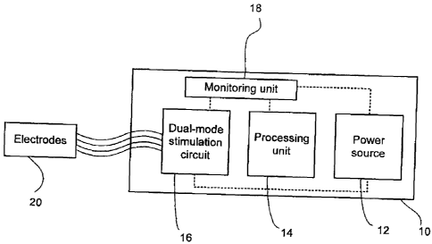
[0011] Figure 1 is a block diagram of an implantable pulse generator
according to an illustrative embodiment of the present invention;
[0012] Figure 2 is a block diagram of a system using the implantable pulse
generator of Figure 1;
[0013] Figure 3 is a block diagram of a prior art H-bridge based current
stimulation circuit;
[0014] Figure 4 is a block diagram of a prior art H-bridge based voltage
stimulation circuit;
[0015] Figure 5 is a block diagram of a first illustrative embodiment of the
dual-mode stimulation circuit of Figure 1;
[0016] Figure 6 is a block diagram of a second illustrative embodiment of the
dual-mode stimulation circuit of Figure 1;
[0017] Figure 7 is a block diagram of a third illustrative embodiment of the
dual-mode stimulation circuit of Figure 1;
[0018] Figure 8 is a block diagram of a fourth illustrative embodiment of the
dual-mode stimulation circuit of Figure 1;
[0019] Figure 9 is a block diagram of a fifth illustrative embodiment of the
dual-mode stimulation circuit of Figure 1;
[0020] Figure 10 is a block diagram of a prior art voltage source with current
feedback;
[0021] Figure 11 is a block diagram of a prior art current source;
[0022] Figure 12 is a block diagram of a prior art unidirectional current
source;
[0023] Figure 13 is a block diagram of a dual-mode source;
[0024] Figure 14 is a block diagram of a saturable current source;
[0025] Figure 15 is a block diagram of a dual-mode source based on the
saturable current source of Figure 14;
CA 02661118 2009-02-19
WO 2008/049199 PCT/CA2007/001787
[0026] Figure 16 is a block diagram of a dual-mode source system based on
the dual-mode source of Figure 14;
10027] Figure 17 is a block diagram of a dual-mode source system based on
the dual-mode source of Figure 15; and
[0028] Figure 18 is a block diagram of the monitoring unit 18 of Figure 1.
DEFINITIONS
[0029] The detailed description and figures refer to the following terms which
are herein defined:
Electrode: any interface such as, for example, an electrode, a lead, a probe,
a
nerve cuff, etc., that may be used to electrically connect a device to
a tissue.
Tissue: any biological tissue such as, for example, muscle, nerve, etc., that
may benefit from therapeutic electrical signals.
DETAILED DESCRIPTION
[0030] Generally stated, non-limitative illustrative embodiments of the
present invention overcome the deficiencies of the prior art implantable pulse
generators (IPG) by providing an IPG which can provide current and/or voltage
stimulation signals to tissues of a subject. This is particularly of interest
as it
precludes using more than one IPG when both current stimulation and voltage
stimuiation are required, or may be required in the future, to dispense
treatment.
[0031] To this end, with reference to Figure 1, an IPG 10 includes a power
source 12 that feeds a processing unit 14, which in turn controls at least one
dual-
mode stimulation circuit 16 that may be connected to at least two electrodes
20 (or
channels on a nerve cuff) adapted to be connected to tissues of a subject (not
shown). The IPG 10 also includes a monitoring unit 18, which provides feedback
signals that relate to the tissue's electrical characteristics from the dual-
mode
stimulation circuit 16 to the processing unit 14 in order to adjust the
stimulation
provided by the dual-mode stimulation circuit 16.
CA 02661118 2009-02-19
WO 2008/049199 PCT/CA2007/001787
6
[0032] As opposed to the prior art, the dual-mode stimulation circuit 16 may
be independently programmed to output various voltage waveforms at various
amplitudes, thus also giving the IPG 10 the capability to perform voltage
steering
during stimulation. The processing unit 14 is used to program, charge and
control
the dual-mode stimulation circuit 16.
[0033] Since impedance measurements imply voltage measurements when
current stimulation is performed and current measurements when voltage
stimulation takes place, the monitoring unit 18 may monitor the required
signals to
provide impedance measurements. This allows the IPG 10 to measure impedance
for both types of stimulation waveforms.
[0034] Alternatively, the power may be supplied transcutaneously from an
external power generator to the IPG 10 using, for example, inductive coupling
between two coils. In this case, the power source 12 may be, for example, a
coil
with associated circuitry.
[0035] Referring to Figure 2, the IPG 10, together with the electrodes 20
may implanted below the skin 1 of a subject and may communicate with an
external control unit 25 that may be used to configure and/or monitor the
operation
of the IPG 10.
[0036] Alternatively, in the case where the IPG 10 power is provided
transcutaneously, the external control unit 25 may be provided-with a power
generator, coil and associated circuitry so as to transmit power to the power
source 12 through the skin of the subject.
Single-mode stimulation circuit
[0037] Referring to Figures 3 and 4, prior art designs of single-mode
stimulation circuits 30 and 40 commonly make use of H-bridge based current or
voltage sources, respectively, to generate biphasic therapeutic stimulation
waveforms. The single-mode stimulation circuits 30 and 40 may also be used to
produce unipolar waveforms, but in this case simpler circuits may be used in
to
reduce the complexity of the associated IPG.
CA 02661118 2009-02-19
WO 2008/049199 PCT/CA2007/001787
7
[0038] In Figure 3, a control circuit (not shown) is used to control single-
mode stimulation circuit 30 such that the control signal lines 31A and 31 D
close or
open associated switches 32A and 32D while the control signal lines 31 B and
31 C
open or close associated switches 32B and 32C. The configuration signal line
35
is used to set the current level the current source 34 outputs. In some cases,
the
configuration signal line 35 carries digital control signals produced by the
processing unit of the IPG (not shown). In other cases, the configuration
signal line
35 carries an analog signal which sets the value of the current the source 34
outputs.
[0039] In such a configuration, it is important to avoid having the control
signal lines 31A and 31B or 31C and 31D activate their associated switches 32A
and 32B or 32C and 32D at the same time, which would result in the shorting of
the output of the current source 34 and cause unnecessary current to flow,
thus
wasting energy. On the other hand, the control signal lines 31B and 31D may be
both safely used to activate their respective switches 32B and 32D to
discharge
the blocking capacitors 33A and 33B and the stray capacitance of the tissue 2.
Similarly, control signal lines 31A and 31C may both safely be used to
activate
their respective switches 32A and 32C to discharge the blocking capacitors 33A
and 33B and the stray resistance/capacitance of the tissue 2. In practice,
common
IPGs may use multiple pairs of electrodes to provide a treatment, in which
case
the same number of single-mode stimulation circuits 30 would be required.
Alternatively, the same number of H-bridges may be used with a shared current
source 34.
[0040] The single-mode stimulation circuit 40 shown in Figure 4 is obtained
by replacing the current source 34 shown in Figure 3 by a programmable voltage
source 44. Instead of having a controlled current to flow in the tissue 2, it
is a
controlled voltage which is applied across the tissue 2. Apart from that, the
operation of the single-mode stimulation circuit 40 shown in Figure 4 is
similar to
the one of the single-mode stimulation circuit 30 shown in Figure 3, the
control
signal lines 41A, 41B, 41C, 41 D, with associated switches 42A, 42B, 42C, 42D,
blocking capacitors 43A, 43B and configuration signal line 45 behaving in a
similar
CA 02661118 2009-02-19
WO 2008/049199 PCT/CA2007/001787
8
fashion as in the case of single-mode stimulation circuit 30. Both single-mode
stimulation circuits 30 and 40 do not require fast responsive sources 34, 44
that
consume more power to invert the direction of the current that flows in the
tissue 2,
as this task is managed by the much more power efficient H-bridge based
circuits.
[0041] Although the single-mode stimulation circuits 30 and 40 shown in
Figures 3 and 4, respectively, share similar architectures, they are not
interchangeable because of the sources 34, 44 they use. Their use is thus
limited
by the type of stimulation they can provide.
Dual-mode stimulation circuit
[0042] Referring now to Figure 5, there is shown a block diagram of a dual-
mode stimulation circuit 50 according to a first illustrative embodiment of
the dual-
mode stimulation circuit 16 of Figure 1. The dual-mode stimulation circuit 50
shares some common features with the single-mode stimulation circuits 30 and
40
shown in Figures 3 and 4, respectively, namely control signal lines 51 A, 51
B, 51 C,
51 D with associated switches 52A, 52B, 52C, 52D, blocking capacitors 53A, 53B
and configuration signal line 55, with the exception that the current source
34 and
voltage source 44 are replaced by a dual-mode source 54. The dual-mode source
54 may be configured to output a programmable current or voltage level using
the
configuration signal line 55. This capability of sourcing either current or
voltage is
an advantage over the prior art as this allows the production of a single IPG
10
having the capability of providing treatment in either mode of operation, i.e.
a
current or voltage based treatment. A dual-mode source that may be used for
the
dual-mode source 54 will be detailed further on.
[0043] This capability of switching at will from one mode of operation to the
other instead having to surgically remove a prior art IPG operating in a given
mode
from a subject's body to replace it with another prior art IPG operating in
another
mode is desirable as it opens the way to treatments that advantageously
combine
the benefits of stimulating current and voltage waveforms to better adapt
itself to
the evolution of the response of the tissue 2 to the therapeutic waveforms.
Furthermore, the capability to control either the current level or the voltage
level of
CA 02661118 2009-02-19
WO 2008/049199 PCT/CA2007/001787
9
the waveforms the dual-mode source 54 outputs allows impedance measurements
that are based on these two types of signals as opposed to what can be done
with
a single-mode source 34, 44. This capability to evaluate the same
characteristics
with two different methods is another advantage over prior art single-mode
stimulation. circuits 30 and 40 as the comparison of the results obtained may
allow
the detection of discrepancies that might have otherwise been undetected.
[0044] Although the dual-mode stimulation circuit 50 of Figure 5 includes a
single dual-mode source 54, it is to be understood that the dual-mode
stimulation
circuit 50 may include a plurality of H-bridges with multiple dual-mode
sources 54
to provide even more flexibility than what is achieved by the current single-
mode
stimulation circuits 30, 40. Thus, a first group of dual-mode sources 54 may
be
configured to provide current stimulation, while a second group may be
configured
to generate stimulating voltage signals. In such cases, a single IPG 10 may
advantageously be used to administrate a plurality of treatments that may have
otherwise required the use of many prior art single-mode iPGs. Furthermore,
the
capability to individually configure the output level and the output mode of
each
dual-mode source 54 of such embodiments enables multi-mode steering of the
resulting treatment.
[0045] A second illustrative embodiment 60 of the dual-mode stimulation
circuit 16 of Figure 1 is shown in Figure 6, which again shares a similar
architecture with the single-mode stimulation circuits 30 and 40 of Figures 3
and 4,
respectively, namely control signal lines 61A, 6113, 61 C, 61D, with
associated
switches 62A, 62B, 62C, 62D and blocking capacitors 63A, 63B, with the
exception that the current source 34 and voltage source 44 are replaced by a
pair
of dual-mode sources 64A and 64B having respective configuration signal lines
65A and 65B_ The architecture of the dual-mode stimulation circuit 60 further
differs from that of single-mode stimulation circuits 30 and 40 in that each
pair of
switches (62A, 62B) and (62C, 62D) connect to the same end of a load formed by
the blocking capacitors 63A, 63B and the tissue 2 and are fed by an associated
dual-mode source 64A, 64B, respectively, thus forming branches 66A and 66B. A
CA 02661118 2009-02-19
WO 2008/049199 PCT/CA2007/001787
dual-mode source that may be used for the dual-mode sources 64A and 64B will
be detailed further on.
[0046] Figure 6 only shows two branches 66A, 66B for clarity but other
embodiments of the dual-mode stimulation circuit 60 may include multiple
branches. The configuration shown in Figure 6 leads to a dual-mode stimulation
circuit 60 architecture which is more complex than that of the dual-mode
stimulation circuit 50 shown in Figure 5 since two dual-mode souroes 64A, 64B
are
required to drive the same number of switches 62A, 62B, 62C, 62D. However, the
advantages that result from the split of the H-bridge into branches 66A, 66B
is
more evident when multiple branches are considered so as to allow steering of
the
produced stimulation. Thus, it results from the use of the two dual-mode
sources
64A, 64B that the outputs of the dual-mode stimulation circuit 60, which are
in
coritact with tissue 2, may be independently controlled instead of being
coupled to
each other as it is the case where a single dual-mode source controls these
outputs. The dual-mode sources 64A and 64B will be detailed further on.
[0047] A third illustrative embodiment 70 of the dual-mode stimulation circuit
16 of Figure 1 is shown in Figure 7, which is derived from the dual-mode
stimulation circuit 60 of Figure 6, having similar components, namely control
signal
lines 71 B, 71 D, with associated switches 72B, 72D, blocking capacitors 73A,
73B,
dual-mode sources 74A, 74B and configuration signal lines 75A, 75B, with the
exception of the top most switches 62A and 62C being replaced by short
circuits.
A dual-mode source that may be used for the dual-mode sources 74A and 74B will
be detailed further on.
[0048] This dual-mode stimulation circuit 70 is less complex than dual-mode
stimulation circuits 50 and 60 as it only includes one switch 72B and 72D per
branch, respectively, instead of two, i.e. (62A, 62B) and (62C, 62D). To
preserve
the functionality of the dual-mode stimulation circuit 70, the control of the
operation
of its sources 74A and 74B must compensate for the removal of the switches,
i.e.
62A and 62C. A current source, when not outputting a current, is seen by the
load
it is connected to as if it was an open circuit. Hence, the dual-mode
stimulation
circuit 70 of Figure 7 may generate the same therapeutic stimulation signals
as the
CA 02661118 2009-02-19
WO 2008/049199 PCT/CA2007/001787
11
dual-mode stimulation circuit 60 of Figure 6 provided that the configuration
signal
line 75B is such that dual-mode source 74B operates as a current source that
outputs no current each and every time the control signal line 71D forces the
opening of the switch 72D. Conversely, configuration signal line 75A should be
such that dual-mode source 74A operates as a current source that outputs no
current each and every time the control signal line 71B forces the opening of
the
switch 72B.
[0049] Alternative embodiments of dual-mode stimulation circuit 70 of
Figure 7 may include more branches 76A, 76B than shown in Figure 7 in order to
provide the same flexibility and the same advantages as mentioned above for
stimulation circuits based on the dual-mode stimulation circuit 60 of Figure
6.
[0050] A fourth illustrative embodiment 80 of the dual-mode stimulation
circuit 16 of Figure 1 is shown in Figure 8, which includes dual-mode sources
84A,
84B and blocking capacitors 83A, 83B, but no switches. A dual-mode source that
may be used for the dual-mode sources 84A and 84B will be detailed further on.
[0051] - A voltage source that produces zero volts across its outputs is seen
as a short circuit by the load it connects to. Hence, the dual-mode
stimulation
circuit 80 of Figure 8 may produce the same therapeutic stimulation signals as
the
dual-mode stimulation circuit 70 of Figure 7 provided that the configuration
signal
line 85B is such that the dual-source source 84B operates.as a voltage source
that
outputs zero volt each and every time the dual-source 84A is configured to
output
current or voltage waveforms. Conversely, the configuration signal line 85A
should
be such that the dual-mode source 84A acts as a voltage source that outputs
zero
volts whenever the dual-source 84B is configured to output current or voltage
waveforms.
[0052] If the dual-mode sources 84A, 84B are configured so as to sink or
source current when they act as current sources, the dual-mode stimulation
circuit
80 is not limited to situations for which a dual-mode source 84A, 84B has to
be
configured to output zero volts when the other dual-mode source 84A, 84B is
active, provided that the currents that enter the dual-mode source 84A, 84B
add
CA 02661118 2009-02-19
WO 2008/049199 PCT/CA2007/001787
12
up to zero at all time. Thus, multiple combinations of mode of operation may
be
used to produce stimulation signals. For example, having a dual-mode source
84A, 84B that outputs 3 V while the other sinks 20 mA of current would be a
possible configuration. On the other hand, making a dual-mode source 84A, 84B
sink 20 mA whilst the other is asked to output 30 mA would not be feasible
since
more current would be entering the tissue 2 than out of it, i.e. the currents
that
enter the dual-mode source 84A, 84B add up to 10 mA. The processing unit 14 of
the IPG 10 of Figure 1 may be programmed to prevent improper configuration of
the dual-mode source 84A, 84B.
[0053] Since it is possible to control the output voltage of a given dual-
source 84A or 84B of the stimulation circuit 80 while the other dual-source
84B or
84A acts as a current source, it becomes possible to minimize the voltage
across
that current source as it stimulates the tissue 2. The stimulation circuit 80
thus
allows power consumption reduction if the processing unit 14 of the IPG 10 of
Figure 1 is also programmed to minimize the voltage across its dual-mode
sources
84A, 84B when they act as current sources.
[0054] Alternative embodiments of dual-mode stimulation circuit 80 of
Figure 8 may include more branches 86 than shown in Figure 8 in order to
provide
the same flexibility and the same advantages as mentioned above for
stimulation
circuits based on the dual-mode stimulation circuit 70 of Figure 7.
[0055] A fifth illustrative embodiment 90 of the dual-mode stimulation circuit
16 of Figure 1 is shown in Figure 9, which may be used when only a single
therapeutic signal is required. The dual-mode stimulation circuit 90 makes use
of a
single dual-mode differential source 94 that may either operate as a
differential
current source or as a differential voltage source, along with blocking
capacitors
93A, 93B. Because of the differential nature of the source 94, there is no
need to
control the direction of the current when the polarity of the output signal
has to
change.
[0056] Since the dual-mode stimulation circuit 90 includes a single dual-
source differential source 94 and no switch, a simplified version of the
processing
CA 02661118 2009-02-19
WO 2008/049199 PCT/CA2007/001787
13
unit 14 of Figure 1 may be used to produce the configuration signal line 95
signals
used to control the dual-mode differential source 94. The configuration signal
line
95 only has to control the modes of operation and the output level of the dual-
mode differential source 94. When the dual-mode stimulation circuit 90 is
required
to produce a multitude of stimulating signals and/or if steering capabilities
are
expected, an aitemative embodiment that includes multiple dual-mode
differential
sources 94 may be used.
[0057] It should be noted that the purpose of the blocking capacitors 33A,
33B, 43A, 43B, 53A, 53B, 63A, 63B, 73A, 73B, 83A, 83B, 93A and 93B is to
prevent DC leakage into the tissue.
Dual-mode source and other circuits
[0058] Referring to Figure 10, there is shown a block diagram of a prior art
voltage source 100 with current feedback. A digital-to-analog converter (DAC)
101,
controlled by configuration signal line 108, feeds the positive input of an
inverting
amplifier formed by operational amplifier 102, feedback resistors 103A, 103B
and
sensing resistor 104. Provided that the value of the sensing resistor 104 is
kept
small when compared to the output impedance of the differential amplifier 105,
the
impact of the sensing resistor 104 on the performances of the voltage source
100
is minimized because the feedback signal originates from its output 106.
[0059] Since the voltage across the sensing resistor 104 is proportional to
the current delivered by the voltage source 100, having a differential
amplifier 105
measure the voltage across the sensing resistor 104 enables impedance
measurements of the load which is connected to the voltage source 100 that are
based on the ratio of the recorded voltages 106 and 107. The voltage source
100
can either sink or source current. It is to be understood that in the
preceding
description of theimpedance measurements it was assumed that the output 106
was connected to grounded tissue. If this is not the case, then the voltage at
output 106 is to be replaced by the voltage drop across the stimulated tissue.
[0060] Referring to Figure 11, there is shown a block diagram of a prior art
current source 110. A DAC 111, controlled by configuration signal line 118,
feeds
CA 02661118 2009-02-19
WO 2008/049199 PCT/CA2007/001787
14
the positive input of an inverting amplifier formed by operational amplifier
112,
feedback resistors 113A and 113B, sensing resistor 114 and differential
amplifier
115. Provided that the value of the sensing resistor 114 is kept small when
compared to the output impedance of the differential amplifier 115, the impact
of
the sensing resistor 114 performances of the current source 110 is minimized
since the feedback signal originates its output 116. The operational amplifier
112
thus performs current regulation because the feedback signal it processes is
proportional to the output current of the current source 110.
[0061] Furthermore, since the voltage across the sensing resistor 114 is
proportional to the current delivered by the current source 110, having the
differential amplifier 115 measure the voltage across the sensing resistor 114
enables impedance measurements of the load which is connected to the current
source 110 that are based on the ratio of the recorded voltages 116 and 117.
The
current source 110 can either sink or source current. It is to be understood
that in
the preceding description of the impedance measurements it was assumed that
the output 116 was connected to grounded tissue. If this is not the case, then
the
voltage at output 116 is to be replaced by the voltage drop across the
stimulated
tissue.
[0062] Referring to Figure 12, there is shown a block diagram of a prior art
unidirectional current source 120. A DAC 121, controlled by configuration
signal
line 128, feeds the positive input of a voltage-to-current converter formed by
operational amplifier 122, feedback resistors 123A and 123B, sensing resistor
124
and transistor 125. Provided that the values of the feedback resistors 123A
and
123B are kept large when compared to the value of the sensing resistor 124,
the
impact of the feedback resistors 123A and 123B on the performances of the
unidirectional current source 120 is minimized since this makes the current
that
flows in the sensing resistor 124 practically equal to the current the
unidirectional
current source 120 sinks. In order to have both of its inputs at the same
voltage,
the operational amplifier 122 will drive the gate of the transistor 125 in a
way that
forces a current proportional to the output of the DAC 121 to flow from the
output
126 of the unidirectional current source 120 through the sensing resistor 124.
CA 02661118 2009-02-19
WO 2008/049199 PCT/CA2007/001787
[0063] Since the voltage across the sensing resistor 124 is proportional to
the current the unidirectional current source 120 sinks, the measure of both
the
voltage across the sensing resistor 124 and the voltage at the output 126 of
the
unidirectional current source 120 enables impedance measurements of the load
which is connected to the unidirectional current source 120 that are based on
the
ratio of the recorded voltages 126 and 127.
[0064] Although the transistor 125 is shown to be a NMOS transistor in
Figure 12, a NPN transistor or equivalent may be used as well to implement the
unidirectional current source 120. More specifically, since the unidirectional
current
source 120 may only make the current flow from its terminal 146 to the ground,
a
PMOS, a NPN transistor or an equivalent circuit may be used for the transistor
125
if there is a need to output current from the terminal 146, provided that the
feedback resistors 123A, 123B and the sensing resistor 124 are connected to
the
power supply of the circuit instead of being connected to the ground.
[0065] Comparing the circuits of voltage source 100 and current source 110
shown in Figures 10 and 11, respectively, reveals a common architecture, apart
from where the feedback is taken, which may be used as a basis for the dual-
mode source.
[0066] Referring now to Figure 13, there is shown block diagram of a dual-
source 130 that may be used for dual-mode sources 54, 64A, 64B, 74A, 74B, 84A
and 84B of Figures 5, 6, 7 and 8. A DAC 131, controlled by configuration
signal
line 138, feeds the positive input of a voltage-to-current converter formed by
operational amplifier 132, feedback resistors 133A and 133B, sensing resistor
134
and differential amplifier 135. The processing unit 14 of the IPG 10, shown in
Figure 1, may control the mode of dual-source 130, i.e. current or voltage
source
mode, using the mode selection signal line 139S, which toggles the mode
selection switch 139 to obtain either of the voltage or current source
configurations
shown in Figures 10 and 11, respectively. The current source mode is selected
when the switch 139 is connected to the output of the differential amplifier
135
while the voltage mode is selected when the switch 139 is connected to the
output
136 of the dual-mode source 130.
CA 02661118 2009-02-19
WO 2008/049199 PCT/CA2007/001787
16
[0067] Since the voltage across the sensing resistor 134 is proportional to
the current delivered by the dual-source 130, having a differential amplifier
135
measure the voltage across the sensing resistor 134 enables impedance
measurements of the load which is connected to the dual-source 130 that are
based on the ratio of the recorded voltages 136 and 137. The dual-mode source
130 may either sink or source current. It is to be understood that in the
preceding
description of the impedance measurements it was assumed that the output 136
was connected to grounded tissue. If this is not the case, then the voltage at
output 136 is to be replaced by the voltage drop across the stimulated tissue.
[0068] In an alternative embodiment, with reference to Figures 6, 7 and 8,
the use of two dual-mode sources 64A, 64B, 74A, 74B, 84A and 84B may not be
required for some applications. For example, an application may push current
or
voltage from one of the dual-mode source 64A, 64B, 74A, 74B, 84A and 84B (for
example in a diagnostic mode) and replace the other one with a simple current
source such as, for example, the unidirectional current source 120 of Figure
12, for
stimulation in order to provide better power performance. Thus, a dual-mode
source allows the identification of the ideal therapy and another source,
having a
simpler circuit, provides stimulation while also providing power economy.
[0069] In a further altemative embodiment, with reference still to Figures 6,
7
and 8, each pair of dual-mode sources 64A, 64B, 74A, 74B, 84A and 84B may be
replaced, respectively, by a voltage source and a current source. The voltage
source and current source may be controlled by the processing unit 14 in order
to
provide either or both voltage and current stimulation.
[0070] It is to be understood that, although the preceding alternative
embodiments make reference to the dual-mode stimulation circuits 60, 70 and 80
of Figures 6, 7 and 8, which respectively include two dual-mode sources 64A,
64B,
74A, 74B, 84A and 84B, the alternative embodiments may also apply to dual-mode
stimulation circuits having a plurality of dual-mode sources and that the
number of
voltage and current sources need not be equal.
CA 02661118 2009-02-19
WO 2008/049199 PCT/CA2007/001787
17
10079] Referring to Figure 14, there is shown a block diagram of a saturable
current source 140 which includes a DAC 141, controlled by configuration
signal
line 148, feeding the positive input of a voltage-to-current converter formed
by
operational amplifier 142, feedback resistors 143A and 143B, sensing resistor
144
and transistor 145.
[0072] When switch 149 is open, the saturable current source 140 operates
similarly to the unidirectional current source 120 of Figure 12. However, when
the
saturation control signal line 149S causes the saturation switch 149 to be
closed,
the operational amplifier 142 does not receive any more feedback signals and
its
output reaches its positive supply rail because of its very high gain. This
output
being connected to the gate of the transistor 145, the high voltage value it
produces when the switch 149 is closed causes saturation of the transistor
145.
This make the transistor 145 behave like a low value resistor which is in
series
with the sensing resistor 144. Provided that the implementation of the
saturable
current source 140 is such that its output impedance is sufficiently low when
the
switch 149 is closed, the saturable current source 140 may be seen to be as a
current source in parallel with a switch. This offers the advantage of making
use of
a simple low power control switch 149 to achieve the same functionality as a
common current source in parallel with a higher power shorting switch.
[0073] Since the voltage across the sensing resistor 144 is proportional to
the current the saturable current source 140 sinks, the measure of both the
voltage
across the sensing resistor 144 and the voltage at the output 146 of the
saturable
current source 140 enables impedance measurements of the load which is
connected to the saturable current source 140 that are based on the ratio of
the
recorded voltages 146 and 147. It is to be understood that in the preceding
description of the impedance measurements it was assumed that the output 146
was connected to grounded tissue. If this is not the case, then the voltage at
output 146 is to be replaced by the voltage drop across the stimulated tissue.
[0074] Referring to Figure 15, the saturable current source 140 of Figure 14
may be connected in parallel with a voltage source 154, controlled by control
signal line 155, that may be disconnected using switch 152 when it sinks a
CA 02661118 2009-02-19
WO 2008/049199 PCT/CA2007/001787
18
controlled current or outputs a controlled voltage, creating a dual-mode
source
150. Such a dual-mode source 150 may be used for the dual-mode sources 54,
64A, 64B, 74A, 74B, 84A and 84B of Figures 5, 6, 7 and 8. Furthermore, a
controlled current flow from the terminal 146 instead of into the terminal 146
may
be achieved by using a PMOS transistor or an equivalent circuit for the
transistor
145 and connecting the feedback resistors 143A, 143B, the sensing resistor 144
and the switch 149 to the power supply of the circuit.
10075] Since the voltage across the sensing resistor 144 is proportional to
the current the dual-mode source 150 sinks, the measure of both the voltage
across the sensing resistor 144 and the voltage at the output 146 of the dual-
mode
source 150 enables impedance measurements of the load which is connected to
the dual-mode source 150 that are based on the ratio of the recorded voltages
146
and 147. It is to be understood that in the preceding description of the
impedance
measurements it was assumed that the output 146 was connected to grounded
tissue. If this is not the case, then the voltage at output 146 is to be
replaced by
the voltage drop across the stimulated tissue.
[0076] Referring to Figure 16, there is shown a block diagram of a dual-
mode source system 160 which includes four dual-mode sources 130, as shown in
Figure 13. However, instead of using one DAC 131 per dual-mode source 130, the
dual-mode source system 160 may use a single DAC 161, which is coupled to a
multiplexer 162 that feeds a multitude of sample-and-hold circuits 164 that
each
connects to an input V1, V2, V3 and V4 of the dual-mode sources 130. Depending
on the commands received from the processing unit 14 of Figure 1, the control
signals SI, S2, S3 and S4 will instruct the dual-mode sources 130 to operate
in
voltage or current mode when required, whereas control signals CtrIDAC 168,
CtrIMUX 163, and CtrIS&H 165 will synchronize the operation of the DAC 161,
the
multiplexer 162 and the sample-and-hold circuits 164, respectively.
[0077] It is to be understood that although the dual-mode source system 160
shown in Figure 16 includes four dual-mode sources 130, the number of dual-
mode sources 130 may vary according to the desired stimulation.
CA 02661118 2009-02-19
WO 2008/049199 PCT/CA2007/001787
19
[0078] Referring to Figure 17, there is shown a block diagram of a dual-
mode source system 170 which includes four saturable current source based dual-
mode sources 150, as shown in Figure 15. Again, instead of using one DAC 141
per dual-mode source 150, the dual-mode source system 170 uses a single DAC
171, which is coupled to a multiplexer 172 that feeds a multitude of sample-
and-
hold circuits 174 that each connects to an input V1, V2, V3 and V4 of the dual-
mode sources 150. Depending on the commands received from the processing
unit 14 of Figure 1, the control signals CFGI, CFG2, CFG3, CFG4, 31, S2, S3
and
S4 will make the sources operate in voltage, current or saturation mode when
required whereas the control signals CtrIDAC 178, CtrIMUX 173, and CtrlS&H 175
wiii synchronize the operation of the DAC 171, the multiplexer 172 and the
sample
& hold circuits 174.
[0079] It is to be understood that although the dual-mode source system 170
shown in Figure 17 includes four dual-mode sources 150, the number of dual-
mode sources 150 may vary according to the desired stimulation.
[0080] Referring finally to Figure 18, there is shown a block diagram of a
monitoring unit 18 (see Figure 1) that may be used with the dual-mode source
systems 160 and 170 of Figures 16 and 17, respectively. The monitoring unit 18
includes a multiplexer 182 connected to the various monitoring points El, E2,
E3,
E4, V1, V2, V3 and V4 of Figures 16 and 17, and an analog-to-digital converter
(ADC) 184 to feed the processing unit 14 (see Figure 1) and allow the
monitoring
of the electrical characteristics of the stimulated tissue. As the processing
unit 14
samples the monitoring points El, E2, E3, E4, V1, V2, V3 and V4, using the
multiplexer 182 and ADC 184 control signals MUXCtrI 183 and CtrIADC 185,
respectively, it may get a voltage value which is proportional to the voltage
at the
output of the selected dual-mode source 130, 150 or a voltage which is
proportional to the current the selected dual-mode source 130, 150 sink or
output.
[0081] Both the ratio of the voltage at the output of a current source over
the
current the source sinks and the ratio of the voltage a voltage source outputs
over
the current through it's sense resistor provide a measure of the impedance of
the
stimulated tissue.
CA 02661118 2009-02-19
WO 2008/049199 PCT/CA2007/001787
[0082] Although the present invention has been described by way of
particular embodiments and examples thereof, it should be noted that it will
be
apparent to persons skilled in the art that modifications may be applied to
the
present particular embodiment without departing from the scope of the present
invention.