Note: Descriptions are shown in the official language in which they were submitted.
CA 02661977 2014-02-14
92499-67
TITLE: HALL SENSOR TEMPERATURE DRIFT CONTROL
[0001]
FIELD OF THE INVENTION
[0002] The present technology relates to utility meters. More
particularly, the
present technology relates to methodologies and corresponding apparatus for
improved controlling of temperature drift in Hall sensors, such as may be
associated with electricity utility meters.
BACKGROUND OF THE INVENTION
[0003] The general object of metrology is to monitor one or more
selected
physical phenomena to permit a record of monitored events. Such basic purpose
of
metrology can be applied to a variety of metering devices used in a number of
contexts. One broad area of measurement relates, for example, to utility
meters. Such
role may also specifically include, in such context, the monitoring of the
consumption
or production of a variety of forms of energy or other commodities, for
example,
including but not limited to, electricity, water, gas, or oil.
[0004] More particularly concerning electricity meters, mechanical
forms of
registers were historically used for outputting accumulated electricity
consumption
data. Such an approach provided a relatively dependable field device,
especially for
the basic or relatively lower level task of simply monitoring accumulated
kilowatt-hour
consumption. Such basic mechanical form of register was typically limited in
its mode
of output, so that only a very basic or lower level metrology function was
achieved.
Subsequently, electronic forms of metrology devices began
1
CA 02661977 2009-02-26
WO 2008/027453 PCT/US2007/019042
to be introduced, to permit relatively higher levels of monitoring, involving
different
forms and modes of data.
[0005] In the context of electricity meters specifically, for a variety
of
management and billing purposes, it has become desirable to obtain more
sophisticated usage data. Solid state devices provided on printed circuit
boards,
for example, utilizing programmable integrated circuit components, have
provided
effective tools for implementing many of such higher level monitoring
functions
desired in the electricity meter context. In addition to the beneficial
introduction of
electronic forms of metrology, a variety of electronic registers have been =
introduced with certain advantages. Still further, other forms of data output
have
been introduced and are beneficial for certain applications, including wired
transmissions, data output via radio frequency transmission, pulse output of
data,
and telephone line connection via such as modems and/or wireless (such as
cellular) linkups.
[0006] The advent of such variety and alternatives has often required
utility
companies to provide data collection mechanisms wherein appropriate data may
be collected in environments that are increasingly hostile to such data
collection.
For example, electrical noise emanating from sources near electricity meter
sensing functions may constitute a source of error in collected data.
Likewise,
different types of metering and/or monitoring components may have various
thermal sensitivities, accounting for which may become more problematic as the
complexity of associated circuitry and thermal environment fluctuations
increase.
[0007] Electricity meters typically include input circuitry for
receiving voltage
and current signals or levels at the electrical service. Input circuitry of
whatever
type or specific design for receiving the electrical service current signals
is referred
to herein generally as current acquisition circuitry, while input circuitry of
whatever
type or design for receiving the electrical service voltage signals is
referred to
herein generally as voltage acquisition circuitry. There are additional issues
related to the measurement of voltage and current that present their own
problems. One such problem relates to the stability and reliability of the
measured
quantities during operation over a dynamic range of conditions, including
ranging
thermal conditions. Under more or less normal operational conditions, thermal
conditions may vary significantly, and for a variety of reasons. Due to such
fact, it
2
CA 02661977 2009-02-26
WO 2008/027453 PCT/US2007/019042
can be difficult to use simple, reliable approaches for accommodating and/or
compensating for, or otherwise preventing deleterious measurement effects due
to, varying thermal conditions.
[0008] Hall sensors are generally known and often used to measure
magnetic
fields in a wide variety of applications such as in position sensing,
contactless
current sensing, and in electricity metering. In general, and as is well known
to
those of ordinary skill in the art, a Hall sensor is a device with at least
four
contacting electrodes. When biased with a current ('bias) through two of such
electrodes, a Hall sensor delivers between its other two electrodes a voltage
that is
proportional both to the component of the magnetic field perpendicular to the
current trajectory, and to the value of the biasing current (lbias).
[0009] It is a common practice that many Hall sensors are fabricated
using thin-
film technologies, at least in some respects similar to techniques and
technologies
as used with semiconductor processing. However, because of changes in electron
population in the active area of such sensors, the magnetic sensitivities of
such
Hall sensors tends to be temperature dependent.
[0010] In view of the foregoing, it is desired to provide a metrology
technology
that permits the collection of accurate data regardless of the environment in
which
the metrology device is installed, and irrespective of the load under which
the
supply source operates, i.e., to provide a metrology device which is
universally
applicable with respect to environment, particularly as to a varying thermal
environment. In the instance of an electricity meter which makes use of Hall
sensor technology, it is desired to provide method and apparatus for
controlling the
sensitivity temperature drift of such Hall sensor technology at any current
bias
(lbias) chosen therefore.
[0011] While various aspects and alternative embodiments may be known
in
the field of utility metering, no one design has emerged that generally
encompasses the above-referenced characteristics and other desirable features
associated with utility metering technology as herein presented.
3
CA 02661977 2014-12-12
=
92499-67
SUMMARY OF THE INVENTION
[0012] In view of the recognized features encountered in the prior
art and
addressed by the present subject matter, it is desirable to provide an
improved
apparatus and corresponding methodology for filtering temperature-dependent
characteristics and/or variations from collected data signals.
[0013] In a broader aspect, a methodology and corresponding apparatus
are
provided for reducing or removing the effects of temperature from sensed
signals of
interest.
[0014] In one of its simpler forms, the present technology may
advantageously
provide control of temperature-related effects which might otherwise cause
signal error
in the form of signal drift in a sensed signal of interest.
[0015] Another advantageous aspect of the present signal filtering
subject
matter may be that it may be provided by reliable techniques yet utilizing a
minimal
number of components while improving the thermal drift of the magnetic
sensitivity of a
Hall sensor.
[0016] Yet another more specific feature of the present technology is
to provide
method and apparatus which may result in a nulling effect on the thermal drift
of the
magnetic sensitivity of a Hall sensor when operating in conjunction with an
otherwise
desired biasing current value.
[0017] In some aspects, the subject technology may be able to improve the
reliability and stability of the magnetic sensitivity of Hall sensor
technology, so that use
of such improved Hall sensor technology in the context of electricity metering
produces
correspondingly more reliable and more stable metrology data based on the
sensing
outputs of such improved Hall sensor technology.
[0018] One present exemplary embodiment relates to a Hall sensor, with
thermal drift control comprising: a planar cross-shaped semiconductive
material having
a central magnetic field responsive active area portion at a relative center
of outer
perimeter crossed arm portions, said central magnetic field responsive active
area
portion having a top surface; a plurality of electrical contacts coupled to
said outer
perimeter crossed arm portions; a gate electrode coupled to and partially
covering a
portion of said top surface of said central magnetic field responsive active
area portion,
4
CA 02661977 2014-12-12
92499-67
said gate electrode having a geometric center located substantially at a
geometric
center of said Hall sensor; and an electrical conductor coupling said gate
electrode to
one of said plurality of electrical contacts. Additional present embodiments
of such
type may involve such an exemplary Hall sensor further combined with the input
of a
meter, for example, such as an electricity meter.
[0018a] In another aspect of the present invention, there is provided
a self-
biasing Hall sensor, comprising: a planar cross-shaped semiconductive material
having a central magnetic field responsive active area portion at a relative
center of
outer perimeter crossed arm portions; a plurality of electrical contacts
coupled to said
outer perimeter crossed arm portions; a gate electrode coupled to and covering
said
central magnetic field responsive active area portion; and a gate control
external to
said planar semiconductive material; wherein said gate control comprises a
resistive
voltage divider having an input portion thereof coupled to a pair of said
plurality of
electrical contacts and an output portion thereof coupled to said gate
electrode such
that said Hall sensor is self-biased by said plurality of electrical contacts
of said Hall
sensor.
[0019] Another present exemplary embodiment relates to a Hall sensor,
with
thermal drift control, comprising: a planar semiconductive material having,
respectively, a central magnetic field responsive active area portion and
outer
perimeter portions; a plurality of electrical contacts coupled to said outer
perimeter
portions; a gate electrode coupled to and covering said central magnetic field
responsive active area portion; and a gate control voltage supply external to
said
planar semiconductive material, said gate control voltage supply comprising an
amplifier having inputs coupled to a pair of said plurality of electrical
contacts and
having an output responsive to a common mode voltage between said amplifier
inputs;
a voltage divider having a pair of inputs and an output, one of said pair of
voltage
divider inputs being coupled to said output of said amplifier, and said output
of said
voltage divider being coupled to said gate electrode. Likewise, additional
present
embodiments of such type may involve such an exemplary Hall sensor further
combined with the input of a meter, for example, such as an electricity meter.
5
CA 02661977 2014-02-14
92499-67
[0020] Still further present exemplary embodiments equally relate to
subject
methodology. One example of such a present methodology relates to a method for
providing a Hall sensor with improved thermal drift characteristics,
comprising:
providing a planar semiconductive material having a central magnetic field
responsive
active area portion and outer perimeter portions; coupling a plurality of
electrical
contacts to the outer perimeter portions; covering a portion of the central
magnetic
field responsive active area portion with a gate electrode such that a
geometric center
of the gate electrode is located substantially at a geometric center for the
Hall sensor;
providing a gate supply voltage; coupling the gate electrode to the gate
supply voltage;
selecting an operating bias current value for the Hall sensor; and varying
effective
characteristics of the gate electrode so that thermal drift characteristics of
the Hall
sensor are substantially annulled when said operating bias current value is
applied to
the Hall sensor. Optionally, such methodology may further include providing
from
such Hall sensor an output connected to the input of a meter, for example,
such as an
electricity meter.
[0021] Still further present exemplary embodiments equally relate to
subject
methodology. One example of such a present methodology relates to a method for
providing a Hall sensor with improved thermal drift characteristics,
comprising:
providing a planar semiconductive material having a central magnetic field
responsive
active area portion and outer perimeter portions; coupling a plurality of
electrical
contacts to the outer perimeter portions; covering at least a portion of the
central
magnetic field responsive active area portion with a gate electrode coupled;
providing
a gate current supply; coupling the gate electrode to the gate current supply;
selecting
a desired operating bias current value for the Hall sensor; and varying
effective gate
electrode characteristics, whereby thermal drift characteristics of the Hall
sensor may
be at least substantially annulled. Optionally, such methodology may further
include
providing from such Hall sensor an output connected to the input of a meter,
for
example, such as an electricity meter.
[0022] Additional objects and advantages of the present subject
matter are set
forth in, or will be apparent to, those of ordinary skill in the art from the
detailed
6
CA 02661977 2014-02-14
92499-67
description herein. Also, it should be further appreciated that modifications
and
variations to the specifically illustrated, referred and discussed features,
elements, and
steps hereof may be practiced in various embodiments and uses of the present
subject matter. Variations may include, but are not limited to, substitution
of equivalent
-- means, features, or steps for those illustrated, referenced, or discussed,
and the
functional, operational, or positional reversal of various parts, features,
steps, or the
like.
[0023] Still further, it is to be understood that different
embodiments, as well as
different presently preferred embodiments, of the present subject matter may
include
-- various combinations or configurations of presently disclosed features,
steps, or
elements, or their equivalents including combinations of features, parts, or
steps or
configurations thereof not expressly shown in the figures or stated in the
detailed
description of such figures.
[0024] Additional embodiments of the present subject matter, not
necessarily
-- expressed in the summarized section, may include and incorporate various
combinations of aspects of features, components, or steps referenced in the
summarized objects above, and/or other features, components, or steps as
otherwise
discussed in this application. Those of ordinary skill in the art will better
appreciate the
features and aspects of such embodiments, and others, upon review of the
remainder
-- of the specification.
6a
CA 02661977 2009-02-26
WO 2008/027453 PCT/US2007/019042
BRIEF DESCRIPTION OF THE DRAWINGS
[0025] A full and enabling disclosure of the present subject matter,
including the
best mode thereof, directed to one of ordinary skill in the art, is set forth
in the
specification, which makes reference to the appended figures, in which:
[0026] Figure 1 illustrates a previously known configuration of a Hall
sensor
wherein a gate is provided over the active area of the Hall sensor;
[0027] Figure 2 illustrates a previously known configuration of a Hall
sensor
wherein a gate is provided over the active area of the Hall sensor, and
wherein
such gate is connected to a low voltage input of the Hall sensor or Hall cell;
[0028] Figure 3A illustrates a previously known configuration of a Hall
sensor
= wherein a gate is provided over the active area of the Hall sensor, and
wherein
such gate is connected in a particular manner to a low voltage input of the
Hall
sensor or Hall cell;
100291 Figure 3B illustrates a previously known configuration of a Hall
sensor
= wherein a gate is provided over the active area of the Hall sensor, and
wherein
such gate is connected in a particular manner to a voltage divider circuit
which is
directly associated with the Hall sensor or Hall cell and fabricated to the
extent
possible from the same material as the Hall device;
[0030] Figure 4 illustrates an exemplary embodiment of a configuration of a
Hall
sensor provided in accordance with the present subject matter, and wherein a
gate
is provided per present subject matter over only a portion of the active area
or
zone of the Hall sensor or cell, and wherein a particular implementation of
control
for such gate is provided in accordance with the present subject matter;
[0031] Figure 5A illustrates a graph referenced in conjunction with
explaining
relationships between biasing currents and temperature sensitivities of Hall
sensor
configurations provided in accordance with the present subject matter versus
previously known Hall sensor configurations;
[0032] Figure 5B illustrates a graph similar to that of Figure 5A
showing that, in
accordance with present subject matter, substantially identical results as
those
_ represented by present Figure 5A may be obtained through adjustments to the
gate bias;
7
CA 02661977 2009-02-26
WO 2008/027453 PCT/US2007/019042
[0033] Figure 6A illustrates a configuration of a Hall sensor provided
in
accordance with the present subject matter, and wherein a gate is provided in
accordance with an alternative embodiment per present subject matter over only
a
portion of the active area or zone of the Hall sensor or cell, and wherein a
particular implementation of control for such gate is provided in accordance
with
the present subject matter;
[0034] Figure 6B illustrates a configuration of a Hall sensor provided
in
accordance with the present subject matter, and wherein a gate is provided in
accordance with another alternative embodiment per present subject matter over
only a portion of the active area or zone of the Hall sensor or cell, and
wherein a
particular implementation of control for such gate is provided in accordance
with
the present subject matter;
100351 Figure 6C illustrates a configuration of a Hall sensor provided
in
accordance with the present subject matter, and wherein a gate is provided in
accordance with yet another alternative embodiment per present subject matter
over only a portion of the active area or zone of the Hall sensor or cell, and
wherein a particular implementation of control for such gate is provided in
accordance with the present subject matter;
[0036] Figure 6D illustrates a configuration of a Hall sensor provided
in
accordance with the present subject matter, and wherein a gate is provided in
accordance with yet still another alternative embodiment per present subject
matter over only a portion of the active area or zone of the Hall sensor or
cell, and
wherein a particular implementation of control for such gate is provided in
accordance with the present subject matter;
[0037] Figure 7A illustrates a configuration incorporating a Hall sensor in
accordance with the present subject matter, wherein a gate is provided over
the
active area of the Hall sensor, and wherein a particular implementation of
control
for such gate is provided in accordance with the present subject matter in
conjunction with external voltage divider circuitry; and
[0038] Figure 7B illustrates a configuration incorporating a Hall sensor in
accordance with the present subject matter, wherein a gate is provided over
the
active area of the Hall sensor, and wherein a particular implementation of
control
for such gate is provided in accordance with the present subject matter in
8
CA 02661977 2009-02-26
WO 2008/027453 PCT/US2007/019042
conjunction with external voltage divider circuitry including common mode
amplification.
[0039] Repeat use of reference characters throughout the present
specification
and appended drawings is intended to represent same or analogous features,
elements, or steps of the present subject matter.
DETAILED DESCRIPTION OF THE PREFERRED EMBODIMENTS
[0040] As discussed in the Summary of the Invention section, the present
subject matter is particularly concerned with corresponding methodology and
apparatus for improving thermal drift characteristics for the magnetic
sensitivity of
Hall sensor devices and, in particular, for annulling the thermal drift for a
desired
biasing current value used with such Hall sensor devices, for the overall
improvement of a measured or sensed particular signal of interest, such as
used
for example in conjunction with an electricity meter.
[0041] Selected combinations of aspects of the disclosed technology
correspond to a plurality of different embodiments of the present subject
matter. It
should be noted that each of the exemplary embodiments presented and
discussed herein should not insinuate limitations of the present subject
matter.
Features or steps illustrated or described as part of one embodiment may be
used
in combination with. aspects of another embodiment to yield yet further
embodiments. Additionally, certain features may be interchanged with similar
devices or features not expressly mentioned which perform the same or similar
function.
[0042] Moreover, it should be appreciated that, whereas the general
discussion
herein relates more specifically to electricity meters using specific sensor
types
including Hall effect sensors, such particular combined use of the Hall effect
sensor technology is not a limitation of the present technology. In general
the
present technology may be applied to any use or application of Hall sensors,
where elimination or reduction of thermal drift of the magnetic sensitivity of
the Hall
sensor device may be desirable.
9
CA 02661977 2009-02-26
WO 2008/027453 PCT/US2007/019042
[0043] Reference will now be made in detail to presently preferred
embodiments of the subject corresponding methodology and apparatus for
improving thermal drift of magnetic sensitivity of a Hall sensor, including
additional
background discussion of prior Hall sensor technology for further contrast
thereof
with the present subject matter.
[0044] Most Hall sensors are planar devices, Le., the conduction of the
electrons occurs in a very thin plane parallel to the surface of the
semiconductor
device. As known to those of ordinary skill in the art, a Hall sensor
typically is a
device with at least four contacting electrodes. In such configurations, the
biasing
current is applied between two opposite contact electrodes and the Hall
voltage is
measured between two other electrodes on each side of the current path.
Information on preferred Hall device shapes and contact locations is well
known,
such as in the well known textbook "Hall Effect Devices, Second Edition" (ISBN
0750308559) by R. S. Popovic.
[0045] As is also well known to those of ordinary skill in the art, the
output of a
Hall sensor for various voltage biasing conditions reads:
VH =G ,u,, = Vbas.
where G denotes a geometric coefficient related to the aspect ratio
(width/length)
of the Hall sensor, pn is the electron mobility, and B is the magnetic
induction to be
measured.
[0046] Since the electron mobility põ is known to always have a
relatively large
temperature variation, voltage biasing should be avoided when one wants to
obtain
precision magnetic measurements. Therefore, it is understood by those of
ordinary skill in the art that the preferred implementation for precision
magnetic
measurements is controlled current biasing ('bias) conditions, for which the
voltage
output of a Hall sensor is known to read:
VI/ = KH = Ibias'Bz
where KH denotes the so-called cross-sensitivity.
100471 The cross-sensitivity KH is related to ns , the sheet electron
concentration in the current channel at the location between the Hall
contacts, by:
ICH =ye n,
where e is the electron charge.
CA 02661977 2009-02-26
WO 2008/027453 PCT/US2007/019042
[0048] Practically, the temperature dependence of rig, and hence of KH,
can be
made lower than a few 100 ppm/ C for a particular design of the device
parameters. Using, for example, a stabilized biasing current 'bias' the
absolute
magnetic sensitivity is represented by:
vii/ez = KH = I bias.
[0049] Such absolute magnetic sensitivity will show a thermal drift
amounting to
the same amount as that of the cross-sensitivity Kg. However, for some
applications, such remaining thermal drift is still too high as compared to
the
desired or required measurement precision specifications in the considered
temperature range. However, practice of the subject matter otherwise presently
disclosed will, in contrast, provide improvement of the thermal drift of the
magnetic
sensitivity of a Hall sensor, and more peculiarly a method for annulling the
thermal
drift for a desired biasing current value.
[0050] One previously known method for seeking to control the remaining
thermal drift of the magnetic sensitivity is to implement a metal gate over
the active
area of the sensor and adjust the value of the control gate voltage as a
function of
temperature in order to compensate for the thermal drift of the electron
population
in the active area. The intended result is a constant magnetic sensitivity
over
temperature variations. Such a methodology has been mentioned previously in
the scientific literature. See, for example, R. Kyburz, J. Schmid, R.S.
Popovic, H.
Melchior, "High Performance InGaAs/InP Hall Sensors With Low Temperature
Coefficient of the Sensitivity', ESSDERC 93 Proceedings, 655-658 (1993).
[0051] Figure 1 illustrates such a previously known configuration of a
Hall
sensor generally 10, having four representative contacting electrodes
generally 12,
14, 16, and 18, wherein a gate generally 20 is provided over the active area
of the
Hall sensor 10. In practicing such a method with such a Hall sensor
configuration,
the method requires knowledge of the carrier concentration behavior versus
temperature as well as ambient temperature measurement data. In addition,
there
must be provided an external feedback circuit (not shown in Figure 1) used for
correspondingly adjusting (that is, fine tuning) the gate voltage (applied
with
representative element 22) as a function of the ambient temperature data.
11
CA 02661977 2009-02-26
WO 2008/027453 PCT/US2007/019042
Therefore, such known method is relatively complicated, apparatus intensive,
and
somewhat cumbersome to implement.
Figure 2 illustrates a previously known configuration of a Hall sensor
generally 10, wherein a gate generally 20 is provided over the active area of
the
Hall sensor, and wherein in accordance with an alternative prior methodology,
such gate 20 is connected via element 22 to a low voltage input (generally 12)
of
the Hall sensor or Hall cell 10. Such previously known gate-control technique
amounts to a self-biasing of the gate 20 at the "Low" voltage of the Hall
sensor 10.
Such technique allows a good control of the sensitivity versus temperature
without
the need of an external biasing circuit. In FET-like devices, this can be
written as.,
1 VD
¨VT
2
Where VG is the gate voltage, VT an equivalent threshold voltage, and Nips the
voltage drop across the Hall sensor, with:
VDS = Rin x bias
where Rin is the Hall sensor input resistance. By tying the gate to the low
voltage
input of the Hall cell, there is a specific value of current for which the
temperature
dependence of (VG-Vps/2) cancels out the temperature dependence of VT. This is
represented by the "Fully gated sensor" curve in Figure 5A.
[00521 The prior technique represented in conjunction with Figure 2
provides a
relatively good control of sensitivity versus temperature without the need of
an
external biasing circuit (that is, the portion of the circuitry represented by
the free
end of element 22 of Figure 1). However, one limitation of such alternative
technique is that it establishes or sets a unique supply current for which the
magnetic sensitivity is temperature independent. Such zero-drift current value
is
inherently determined by the physical properties of the device and cannot be
chosen independently.
100531 Such limitation on the established zero-drift supply current
value is a
drawback because it may not be the best choice when considering other
properties
or requirements of the sensor. For example, it has been found that such value
12
CA 02661977 2009-02-26
WO 2008/027453 PCT/US2007/019042
may be about 70 microampere for Hall sensors if used in certain electricity
meter
configurations, and such value may be contrary to other needs of such
configuration (for example, too low). Still within previously known solutions,
efforts
have been made to overcome such drawback of the limited bias current approach.
Present Figures 3A and 3B are intended to represent several of such attempted
solutions. Figure 3A illustrates a previously known configuration of a Hall
sensor
generally 10 wherein a gate generally 20 is provided over the active area of
the
Hall sensor 10, and wherein such gate 20 is connected in a particular manner
relative to a low voltage input generally 12 of the Hall sensor or Hall cell
10. More
specifically, instead of connecting the gate at the "Low" contact (the
"Source" if
using field-effect transistor (FET) terminology), Figure 3A shows such
connection
being made at an intermediate point of the channel. In other words, the
connection is made at some intermediate position between the Source and the
Hall sensor arm, as represented by present Figure 3A.
[0054] In such an arrangement as in present Figure 3A, the zero-drift
current
value advantageously will be higher than when otherwise contacting the gate to
the Source. However, such an arrangement requires an extra contact, which
might
destroy the balance of the Hall sensor and create or result in accuracy
problems.
[0055] Representative of another attempt to address such drawback of
the
limited bias current approach, Figure 3B illustrates a previously known
configuration of a Hall sensor generally 10 wherein a gate generally 20 is
provided
over the active area of the Hall sensor 10, and wherein such gate 20 is
connected
in a particular manner to a voltage divider circuit which is directly
associated via
element 22 with the Hall sensor or Hall cell 10, and which is fabricated to
the
extent possible from the same material as the Hall device 10. More
specifically,
the resistors 24 and 26 are used relative to input side connections 12 and 14
of
Hall sensor 10 in a manner well understood by those of ordinary skill in the
art, to
create a bias input for gate 22. To avoid or limit the effects of differential
reactions
to changing thermal conditions, the material for the separate resistors 24 and
26 of
the circuitry illustrated is made in the same material as that of the Hall
sensor 10.
By such an approach to biasing gate 22, the overall thermal drift of the
magnetic
sensitivity of the Hall sensor generally 10 may be improved, but such prior
13
CA 02661977 2009-02-26
WO 2008/027453 PCT/US2007/019042
approach clearly increases the complexity of the configuration and its
associated
implementation.
[00561 Therefore, while the two prior methodologies represented by
present
Figures 3A and 3B provide a relatively acceptable level of improvement to the
'thermal drift characteristics of an associated Hall sensor device, they
create the
drawback of increased overall complexity of the resulting Hall device.
100571 In accordance with present technology, a methodology has been
developed whereby the effect imparted by a gate electrode may be varied to
annul
thermal effects within the Hall sensor. In some embodiments of the present
subject matter, the gating effect may be varied by physically varying the gate
electrode. In other embodiments the gating effect may be varied by varying the
control voltage applied to the gate electrode. In further embodiments,
combinations of the first and second embodiments may be employed.
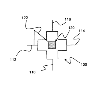
[0058J Figure 4 illustrates an exemplary embodiment of a configuration
of a Hall
sensor generally 100 provided in accordance with the present subject matter,
and
wherein a gate generally 120 is provided per present subject matter over only
a
portion of the active area at the center of the Hall sensor or cell 100 cross,
and
wherein a particular implementation of control for such gate is provided per
element 122 in accordance with the present subject matter.,, The exemplary
embodiment of present Figure 4 makes use of a gate-control technique that
amounts to a self-biasing of the gate 120 associated with the low voltage
input
generally 112 of the Hall sensor 100. While incorporating such particular gate-
control technique, the gate control is itself in an overall combination with a
gate
120 that is fundamentally different from the gate 20 of present Figure 2. As a
result, the Figure 4 illustrated embodiment in accordance with the present
subject
matter is free from the limitation on the drift canceling bias current value
that is a
substantial drawback to the prior approach represented by such Figure 2. In
addition, the present subject matter of Figure 4 results in the advantage of
relatively more simple and robust implementation.
[0059] In comparison with the gate 20 of the Figure 2 prior configuration,
the
present subject matter of Figure 4 makes use instead of a gate 120 which may
be
thought of from one perspective as a partial gate, i.e., a gate 120 covering
only a
14
CA 02661977 2009-02-26
WO 2008/027453 PCT/US2007/019042
fractional portion of the active area at the relative center of the crossed
elements
forming the Hall device, as represented in such present Figure 4.
[0060] The graphs of present Figures 5A and 5B assist to illustrate
pertinent
present aspects of temperature sensitivity control for present versus prior
Hall
sensor configurations. As represented in such Figure 5A graph, temperature
sensitivity ST is displayed in units of PPM (parts per million) per degree
Centigrade
versus operating bias current 'bias in units of microamperes. For clarity, the
three
response lines shown on the graph of present Figure 5 are not additionally
labeled
with numbers but are with descriptions.
[0061] Those of ordinary skill in the art will understand that one of the
response
lines of Figure 5A (labeled "Standard gateless sensor") has no slope while two
of
such lines do have a slope. The line without any slope has a single
intersection
point on the vertical axis, which is a number offset from zero (in this
instance,
significantly below zero). While the other two lines do have a slope, one
(labeled
"Fully gated sensor") has a slope in this instance much higher than the other
(labeled "Partially gated sensor").
[0062] The graphic illustrations of present Figure 5A represent that a
standard
(that is, prior art) gateless Hall sensor can be operated at any bias current
'bias, but
with no control over ST. In comparison, a Hall sensor gated in accordance with
the
prior art (that is, a "Fully gated sensor" but without other features in
accordance
with the present subject matter) has a single operating bias current !bias for
which
ST = 0. In contrast with both such prior art arrangements, an arrangement in
accordance with at least one exemplary embodiment of the present subject
matter
(in other words, a "Partially-gated" Hall sensor) will also have a single
operating
point for which Si = 0, but such value advantageously corresponds to a
relatively
higher bias current 'bias than that of the above-referenced "Fully gated
sensor."
10063] As an additional feature in accordance with the present subject
matter,
such bias current 'bias operating point of the present "Partially gated" Hall
sensor
embodiments can advantageously be chosen (that is, specified) by tuning the
fraction of the active area that is gated. Therefore, the descriptive language
included on present Figure 5A reflects that "Partially gated" Hall sensor
embodiments in accordance with the present subject matter have a "Tunable
CA 02661977 2009-02-26
WO 2008/027453 PCT/US2007/019042
operating point" while the prior art arrangements of the "Fully gated sensor'
approach have a "Fixed operating point."
[0064] In such present "Partially gated" Hall sensor embodiments, the
overall
temperature dependence of the Hall sensor is now the average of the gated and
ungated zones. Changing by design the fraction of gate coverage, the unique
zero-
thermal-drift supply current can therefore be set as desired, or as needed for
a
particular embodiment or set of design criteria. Therefore, in accordance with
present apparatus and methodology, those of ordinary skill in the art
practicing the
present subject matter may now first determine and select a supply current
optimized per the overall needs of the implementation, and then subsequently
adjust or tune the coverage size of the gate surface over and relative to the
active
area of the Hall sensor, in order to have a magnetic sensitivity that is
independent
of temperature, even while operating at the optimum supply current. Therefore,
the present methodology and corresponding apparatus has the advantage of
simplicity over prior methods (that is, no extra components or circuits
required),
even if for the same or similar final results.
[0065] With reference now to Figures 5B and 7A, a second embodiment of
the
present subject matter will be described. As may be seen from a comparison of
Figures 5A and 5B, the illustrated curves are substantially identical with the
exception of notations. Where, for example, in Figure 5A, one of the curves is
labeled "Fully gated sensor," a corresponding curve in Figure 5B is labeled
agate
biased at low input voltage. Likewise, the curve labeled "Partially gated
sensor" in
Figure 5A finds its corresponding curve in Figure 5B listed as "gate biased
using a
voltage divider." The illustration of such two Figures shows that
substantially the
same results may be obtained for the two embodiments of the present subject
matter by employing slightly different techniques for arriving at the same
effective
operating point.
[0066] In other words, the first embodiment of the present subject
matter
provides a tunable operating point based on adjustments in the coverage area
of
the gating electrode. In the second embodiment of the present subject matter,
the
coverage area of the gating electrode may be fixed and the voltage applied may
be
varied to achieve a preselected tunable operating point. Of importance to the
second method, however, is the source of the voltage applied to the gating
16
CA 02661977 2009-02-26
WO 2008/027453 PCT/US2007/019042
electrode, as will be explained more fully with reference to Figure 7A. It
should, of
course, be appreciated by those of ordinary skill in the art that a
combination of the
first and second embodiments could be provided so that fine tuning of
individual
sensors could be achieved by a combination of voltage adjustment and gating
electrode trimming.
[0067] Figures 6A through 6D illustrate various exemplary
configurations of Hall
sensors provided in accordance with the present subject matter, and wherein
respective gates are provided in accordance with respective alternative
embodiments per present subject matter over only a portion of the active area
or
zone of the Hall sensor or cell, and wherein a particular implementation of
control
for such gate is provided in accordance with the present subject matter. As in
Figure 4, corresponding aspects (albeit different in part from the prior art
to present
embodiments) are shown by reference characters which use their own hundred-
series designation, as will be understood by those of ordinary skill in the
art. While
reference characters for Figure 4 were the hundred series, Figures 6A through
6D
are the two hundred series through five hundred series, respectively.
Similarly,
Figures 7A and 7B reference characters are the six hundred series and seven
hundred series, respectively. In view of the foregoing, repetitive discussion
of
reference characters is reduced for the convenience of the reader.
[0068] In the exemplary embodiment of present Figure 6A, gate 220 has an
alternative shape in the form of the letter "X", or that of a cross-shape
which is
partially rotated in top view, such as by about 45 degrees. In the exemplary
embodiment of present Figure 6B, gate 320 is cross-shaped, and overlapping
with
the generally cross-shaped active area or region portion of Hall device
generally
300. However, as illustrated, gate 320 is generally smaller that the cross-
shaped
active area of Hall device 300, so that that gate only partially covers such
active
area, in keeping with the features of the present embodiments also represented
in
present Figures 4 and 6A. In the exemplary embodiment of present Figure 6C,
gate 420 assumes yet another alternative shape in accordance with the present
subject matter. In this instance, such gate 420 assumes several or plural,
additionally partial gate components, collectively only partially covering the
active
area of Hall device 400 (again in accordance with such present exemplary
embodiments). In the exemplary embodiment of present Figure 6D, gate 520
17
CA 02661977 2014-02-14
92499-67
assumes yet still another alternative shape in accordance with the present
subject
matter, although still generally cross-shaped as in Figures 6A and 6B. In this
instance,
gate 520 more nearly resembles gate 220 of Figure 6A but provides a more
nearly star
or multi-triangular shaped formation, allowing yet still another exemplary
variation in
active area coverage area.
[0069] While the exemplary embodiments of such Figures 6A through 6D,
respectively, illustrate various optimized gate designs, different variations
may be
practiced. It is believed, however, that the better performing of such
alternative
designs per the present subject matter, symmetrical gate designs are
preferred, and
the active area of the corresponding Hall device should preferably be
completely
partitioned by the gate component or components.
[0070] Figure 7A illustrates a configuration incorporating a Hall
sensor generally
600 in accordance with yet another exemplary embodiment of the present subject
matter. In such exemplary arrangement, a gate generally 620 is provided over
the
entirety of the active area of the Hall sensor 600. However, a particular
implementation of control for such gate 620 is provided in accordance with the
present
subject matter. In accordance with such present subject matter, such gate
control is
provided in conjunction with external voltage divider circuitry generally 628.
[0071] While Figure 7A makes uses of a gate-control voltage-divider
solution
somewhat similar to the prior arrangement of prior Figure 3B, such present
arrangement is nonetheless different from the prior arrangement. For example,
the
voltage-divider subject matter generally 628 of present Figure 7A is external
to the
chip or component within which Hall device 600 (as otherwise illustrated by
separate
designation of chip 628') is otherwise implemented. Such voltage-divider
subject
matter generally 628 of present Figure 7A, having its own resistors 624 and
626, is
also a relatively high resistance implementation (at least as compared with
the
resistors 24 and 26 more directly implemented with Hall sensor 10 in the
previously
existing arrangement of present Figure 3B).
[0072] Such combined present features of present Figure 7A, inclusive
of the
use of relatively very high resistances, avoids the constraint or drawback of
the prior
art of attempting to establish the same temperature coefficient for the
voltage-
18
CA 02661977 2009-02-26
WO 2008/027453 PCT/US2007/019042
divider circuitry as that of the Hall cell resistance. The resulting high
resistance
arrangement of present Figure 7A makes the current flowing through the voltage-
divider 628 negligible, and therefore any difference in temperature
coefficients is
removed as a consideration of any importance.
[0073] With reference now to Figure 7B, a further embodiment of the present
subject matter will be described. As may be seen by comparison of Figures 7A
and 7b the two Hall sensor configurations are substantially similar except for
at
least two features. The first such feature is readily apparent from the
schematic
illustrations and corresponds to the inclusion of an amplifier 752. The second
feature is less apparent and resides in the fact that in the embodiment of
Figure
7A, resistors 724, 726 forming voltage divider 728 are constructed separately
from
the Hall sensor while in the embodiment of Figure 7B resistors 744, 746 may be
included on the Hall sensor chip.
[0074] With respect to the embodiment of Figure 7B, it will be
appreciated that
amplifier 752 is configured to provide a signal at its output line 758 based
on a
common mode voltage at input terminals 754, 756 derived from the input
voltages
to the Hall sensor at its terminals 718, 716. An important aspect of such
configuration resides in the fact that, with the inclusion of amplifier 752,
the device
requires no trimming of either the gating electrode or the voltage divider,
but rather
the adjustment function is automatically carried out by adjustment of the
voltage
divider input voltage as a result of the common mode operation associated with
amplifier 752.
While the present subject matter has been described in detail with respect
to specific embodiments thereof, it will be appreciated that those skilled in
the art,
upon attaining an understanding of the foregoing may readily produce
alterations
to, variations of, and equivalents to such embodiments. For example, the
embodiments illustrated and described with respect to Figures 7A and 7B may
also
be further modified using the techniques disclosed with respect to Figures 6A-
6D.
Further, it should be noted that the technology herein disclosed is not
incompatible
with known spinning current methodologies used to remove effects of offset and
noise in certain Hall sensor configurations. Accordingly, the scope of the
present
disclosure is by way of example rather than by way of limitation, and the
subject
disclosure does not preclude inclusion of such modifications, variations
and/or
19
CA 02661977 2009-02-26
WO 2008/027453
PCT/US2007/019042
additions to the present subject matter as would be readily apparent to one of
ordinary skill in the art.