Note: Descriptions are shown in the official language in which they were submitted.
CA 02662202 2009-02-27
FP07-0197-00
DESCRIPTION
CONDUCTIVE ADHESIVE FILM AND SOLAR CELL MODULE
Technical Field
[0001] The present invention relates to a conductive adhesive film and
to a solar cell module.
Background Art
[0002] Solar cell modules have a construction wherein a plurality of
photovoltaic cells are connected in series and/or in parallel via wiring
members that are electrically connected to their surface electrodes.
Solder has traditionally been used for connection between photovoltaic
cell surface electrodes and wiring members during the fabrication of
such solar cell modules (see Patent documents 1 and 2, for example).
Solder is widely used because of its excellent connection reliability,
including conductivity and anchoring strength, low cost and general
applicability.
[0003] Wiring connecting methods that do not employ solder are
known, such as connecting methods using conductive adhesives and
connecting methods using conductive films (see Patent documents 3-6,
for example).
[0004] [Patent document 1] Japanese Unexamined Patent Publication
No. 2004-204256
[Patent document 2] Japanese Unexamined Patent Publication No.
2005-050780
[Patent document 3] Japanese Unexamined Patent Publication No.
2000-286436
[Patent document 4] Japanese Unexamined Patent Publication No.
1
CA 02662202 2012-05-10
27986-87
2001-357897
[Patent document 5] Japanese Patent Publication No. 3448924
[Patent document 6] Japanese Unexamined Patent Publication No.
2005-101519
Disclosure of the Invention
[0005] When connecting photovoltaic cell surface electrodes and wiring
members using solder, given a solder melting temperature of generally
about 230-260 C, the high temperature of connection and the volume
shrinkage of the solder adversely affect the photovoltaic cell
semiconductor structure, often resulting in deteriorated characteristics of
the photovoltaic cells.
[0006] In addition, due to the properties of solder with solder
connections, it is difficult to control the thickness at the connection
interface with the adherend, and this has been an obstacle to sufficient
dimensional precision for packages. When sufficient dimensional
precision cannot be achieved, product yield tends to be reduced during
the packaging process.
[0007] Even when connection is established between the photovoltaic
cell surface electrodes and wiring members using a conductive adhesive
as described in Patent documents 3-5, adequate connection reliability is
not always achieved and the characteristics can undergo significant
deterioration with time under high-temperature, high-humidity
conditions.
[0008] Furthermore, although bonding can be achieved at low
temperature when a conductive film is used for connection between the
2
CA 02662202 2012-05-10
27986-87
photovoltaic cell surface electrodes and wiring members and described in
Patent
document 6, thus minimizing the adverse effects on photovoltaic cells that
result
when solder is used, the connection reliability is not always sufficient
because effects
of the surface condition of the adherend are not taken into account.
[0009] The present invention provides a conductive adhesive film which is
used for connection of photovoltaic cells on a single-crystal, polycrystalline
or
amorphous silicon wafer or compound semiconductor wafer via wiring members,
which allows connection between the photovoltaic cell surface electrodes and
wiring
members to be established without adversely affecting the photovoltaic cells
and
which allows satisfactory connection reliability to be achieved, as well as a
solar cell
module employing it.
[0010] The invention provides a conductive adhesive film for electrical
connection between photovoltaic cell surface electrodes and wiring members,
which
comprises an insulating adhesive and conductive particles and has a (t/r)
value in the
range of 0.75-17.5, where r ( m) is the mean particle size of the conductive
particles
and t ( m) is the thickness of the conductive adhesive film, wherein the
content of
conductive particles is 1.7-15.6 vol% based on the total volume of the
conductive
adhesive film.
[0011] The conductive adhesive film of the invention having such a
construction allows connection to be established between photovoltaic
3
CA 02662202 2009-02-27
FP07-0197-00
cell surface electrodes and wiring members without adversely affecting
the photovoltaic cells, and can provide satisfactory connection
reliability.
[0012] The insulating adhesive in the conductive adhesive film of the
invention preferably contains a rubber component at 9-34 mass% based
on the total mass of the insulating adhesive.
[0013] The elastic modulus of the conductive adhesive film of the
invention is preferably 0.5-4.0 GPa.
[0014] Also, the shapes of the conductive particles in the conductive
adhesive film of the invention are preferably burr-shaped or spherical.
[0015] The invention further provides a solar cell module having a
construction with a plurality of photovoltaic cells with surface
electrodes connected via wiring members electrically connected to their
surface electrodes, wherein the surface electrodes and wiring members
are connected by a conductive adhesive film according to the invention.
[0016] Since this type of solar cell module has photovoltaic cell surface
electrodes and wiring members connected using a conductive adhesive
film of the invention as described above, there is no adverse effect on
the photovoltaic cells and sufficient connection reliability is achieved.
Effect of the Invention
[0017] According to the invention it is possible to provide a conductive
adhesive film which allows connection to be established between
photovoltaic cell surface electrodes and wiring members without
adversely affecting the photovoltaic cells, and can provide satisfactory
connection reliability, as well as a solar cell module employing the same.
Brief Description of the Drawings
4
= CA 02662202 2009-02-27
FP07-0197-00
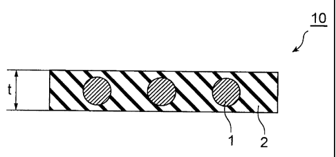
[0018] Fig. 1 is a schematic cross-sectional view showing an
embodiment of a conductive adhesive film according to the invention.
Fig. 2 is a set of illustrations showing the states of connection between
adherends when using conductive adhesive films with different (t/r)
values.
Fig. 3 is a schematic view of the essential portion of a solar cell module
according to the invention.
Fig. 4 is a graph showing the relationship between the ratio of the film
thickness t of the conductive adhesive film and the mean particle size r
of the conductive particles ((film thickness t/particle size r), and the
change in fill factor (F.F.) after 500 hours in an 85 C, 85% RH
atmosphere {F.F.(500 h)/F.F.(0 h)}.
Explanation of Symbols
[0019] 1: Conductive particles, 2: insulating adhesive, 3: surface
electrode, 3a: bus electrode (surface electrode), 3b: bus electrode
(surface electrode), 4: wiring member, 6: semiconductor wafer, 7: finger
electrode, 8: rear electrode, 10: conductive adhesive film, 100: solar cell
module.
Best Mode for Carrying Out the Invention
[0020] Preferred embodiments of the invention will now be explained
in detail, with reference to the accompanying drawings. Identical or
corresponding parts in the drawings will be referred to by like reference
numerals and will be explained only once.
[0021] Fig. 1 is a schematic cross-sectional view showing an
embodiment of a conductive adhesive film according to the invention.
As shown in Fig. 1, the conductive adhesive film 10 of the invention
5
CA 02662202 2009-02-27
FP07-0197-00
comprises at least conductive particles 1 and an insulating adhesive 2.
[0022] The conductive adhesive film 10 of the invention serves to
connect photovoltaic cell electrodes and wires (wiring members) used to
link the solar cells in series and/or in parallel. Electrodes (surface
electrodes) are formed on the front and back sides of the photovoltaic
cell to withdraw energy.
[0023] The surface electrodes may be made of known materials capable
of electrical conduction, and as examples there may be mentioned
common silver-containing glass paste, or silver paste, gold paste, carbon
paste, nickel paste or aluminum paste obtained by dispersing conductive
particles in adhesive resins, and ITO formed by firing or vapor
deposition. Silver-containing glass paste electrodes are preferred
among these from the viewpoint of heat resistance, conductivity,
stability and cost.
[0024] Photovoltaic cells generally have an Ag electrode and an Al
electrode each formed as surface electrodes by screen printing or the
like, on a substrate composed of at least one or more Si single-crystal,
polycrystal or amorphous materials.
[0025] The electrode surfaces usually have irregularities with a surface
roughness (ten-point average surface roughness Rz) of 3-30 pm. In
most cases, the electrodes formed on the photovoltaic cells are rough,
with a surface roughness Rz of 8-18 m. As a result of much ardent
research, the present inventors have found that the connection reliability
deteriorates in conventional conductive adhesive compositions and
conductive films because of these irregularities.
[0026] That is, without small conductive particle sizes and suitable
6
CA 02662202 2009-02-27
FP07-0197-00
contents in electrode surfaces with irregular shapes, the particles
become embedded in the recesses of the electrode surfaces resulting in
inadequate conductivity. Moreover, when the thickness of the coated
film formed using a conductive adhesive composition or conductive
film is smaller than the difference in elevation of the irregularities on
the electrode surface, it becomes impossible to obtain sufficient
adhesion with adherends and the connection reliability is thus reduced.
[0027] Furthermore, an excessive coated film thickness with respect to
the conductive particle sizes interferes with sufficient elimination of the
resin of the conductive particles surface during thermocompression
bonding, thus reducing the conductivity. If the ratio of the mean
particle size r (pm) of the conductive particles and the thickness t (1.tm)
of the coated film that is formed (coated film thickness t/conductive
particle mean particle size r) is less than 0.75, filling with the adhesive
component becomes insufficient and poor connectivity is likely to result.
[0028] The present inventors have found that sufficient connection
reliability between adherends is largely dependent on the ratio between
the particle sizes (mean particle size) of the conductive particles
dispersed in the insulating adhesive component and the thickness of the
coated film that is formed (the conductive adhesive film thickness)
between the conductive adhesive film and the irregularities on the
electrode surface.
[0029] The thickness of the conductive adhesive film specified
according to the invention may be measured using a micrometer. The
mean particle size of the conductive particles may be the average of the
particle sizes of 20 measured particles when the conductive particles are
7
CA 02662202 2009-02-27
FP07-0197-00
observed at 3,000x using a scanning electron microscope (SEM).
[0030] The conductive adhesive film 10 of the invention must have a
ratio between the mean particle size r (pm) of the conductive particles in
the conductive adhesive film 10 and the thickness t (gm) of the
conductive adhesive film 10 (film thickness t/mean particle size r) of
0.75-17.5, and the content of the conductive particles 1 in the
conductive adhesive film 10 must be 1.7-15.6 vol% based on the total
volume of the conductive adhesive film 10.
[0031] If the ratio between the mean particle size r of the conductive
particles 1 and the thickness t of the conductive adhesive film 10 (t/r) is
0.75-17.5 and the content of the conductive particles 1 is 1.7-15.6 vol%
based on the total volume of the conductive adhesive film 10,
conductivity will be achieved between the particles even if one of the
conductive particles becomes buried in a recess on the adherend surface,
thus helping to ensure sufficient electrical connection between the
adherends.
[0032] Fig. 2 is a set of illustrations for explanation of connection
between adherends when using conductive adhesive films. Figs. 2(a)
to (d) show connection states when using conductive adhesive films
with different (fir) values, and specifically when using a conductive
adhesive film 20 with a (fir) value of 1-17.5 (Fig. 2(a)), a conductive
adhesive film 30 with a (fir) value of at least 0.75 and less than 1 (Fig.
2(b)), a conductive adhesive film 40 with a (fir) value of less than 0.75
(Fig. 2(c)) and a conductive adhesive film 50 with a (fir) value of
greater than 17.5 (Fig. 2(d)). The adherends used were a photovoltaic
cell surface electrode 3 and a wiring member 4 for connection between
8
CA 02662202 2009-02-27
FP07-0197-00
photovoltaic cells, and the surface electrode 3 had irregularities on the
surface. Fig. 2 also shows a case where the conductive adhesive film
is situated between the adherends and connection is established by
thermocompression bonding.
[0033] When using the conductive adhesive film 20 shown in Fig. 2(a),
the irregularities on the surface electrode 3 can be sufficiently filled
with the conductive particles 1 and bonding and electrical connection
between the surface electrode 3 and wiring member 4 can be
satisfactorily established. When using the conductive adhesive film 30
shown in Fig. 2(b), the conductive particles 1 become deformed and
embedded in the surface electrode and the irregularities on the surface
electrode 3 can be sufficiently filled with the conductive particles 1, so
that bonding and electrical connection between the surface electrode 3
and wiring member 4 can be satisfactorily established.
[0034] When using the conductive adhesive film 40 shown in Fig. 2(c),
on the other hand, the mean particle size of the conductive particles 1 is
too large with respect to the thickness of the film, and therefore even
with deformation of the conductive particles 1 or their embedding into
the surface electrode, the insulating adhesive 2 and wiring member 4
fail to come into contact and bonding cannot be achieved. When using
the conductive adhesive film 50 shown in Fig. 2(d), the mean particle
size of the conductive particles 1 is too small with respect to the
thickness of the film, and therefore the conductive particles 1 fill the
recesses of the surface electrode 3, making it impossible to ensure
electrical connection.
[0035] Thus, limiting the value of (t/r) for the conductive adhesive film
9
CA 02662202 2009-02-27
FP07-0197-00
to within the range of 0.75-17.5 can guarantee satisfactory connection
between adherends. From the viewpoint of obtaining even more
satisfactory connection between adherends, the value of (t/r) is
preferably 1.0-12.0 and more preferably 2.0-9Ø
[0036] The conductive adhesive film 10 of the invention comprises at
least an insulating adhesive component 2 and conductive particles 1.
There are no particular restrictions on the insulating adhesive
component 2, but a thermosetting resin is preferably used from the
viewpoint of connection reliability.
[0037] Any publicly known thermosetting resin may be used, examples
of which include epoxy resins, phenoxy resins, acrylic resins, polyimide
resins, polyamide resins, polycarbonate resins and the like, although one
or more from among epoxy resins, phenoxy resins and acrylic resins are
preferred from the viewpoint of obtaining more adequate connection
reliability.
[0038] From the viewpoint of the resin flow property and control of the
physical properties of the film, the conductive adhesive film 10
preferably contains a rubber component as the insulating adhesive
component 2. Any publicly known rubber component may be used,
examples of which include acrylic rubber, butyl rubber, silicone rubber,
urethane rubber, fluorine rubber and the like, although acrylic rubber is
preferred from the viewpoint of miscibility with the thermosetting resin,
and adhesiveness with the adherends.
[0039] The rubber component content is preferably 9-34 mass% based
on the total mass of the insulating adhesive component 2. A rubber
component content of 9-34 mass% based on the total mass of the
10
CA 02662202 2009-02-27
FP07-0197-00
insulating adhesive component 2 will result in excellent adhesiveness
between the conductive adhesive film 10 and adherends, while also
providing a satisfactory shape following property for physical variation
in the adherend due to environmental changes, and sufficient
minimization of defective connections between adherends.
[0040] There are no particular restrictions on the conductive particles 1,
and for example, gold particles, silver particles, copper particles, nickel
particles, gold-plated particles, copper-plated particles and nickel-plated
particles may be mentioned. The conductive particles 1 are preferably
burr-shaped or spherical from the viewpoint of sufficiently filling the
surface irregularities of the adherend during bonding and adequately
ensuring electrical connection between adherends. Specifically, burr-
shaped or spherical conductive particles 1 are preferred because they
can sufficiently fill irregularities even on adherend surfaces with
complex irregular shapes, and because the shape following property of
such conductive particles 1 is higher for variation caused by vibration or
expansion after connection.
[0041] The mean particle size r of the conductive particles 1 is not
particularly restricted so long as it is a mean particle size such that the
value of (t/r) is in the range of 0.75-17.5, but it is preferably 2-30 pm
and more preferably 10-20 p.m. It will be possible to achieve more
satisfactory adhesion and conduction between adherends especially
when the adherend surface roughness Rz is in the range of 3-30 pm
(more preferably 8-18 pm) and the mean particle size of the conductive
particles 1 is within the aforementioned range. The mean particle size
r of the conductive particles 1 with respect to the surface roughness of
11
CA 02662202 2009-02-27
FP07-0197-00
the adherend is preferably at least 1/2 Rz, more preferably at least Rz
and even more preferably at least Ry (ten-point average surface
roughness: Rz, maximum height: Ry).
[0042] The content of the conductive particles 1 in the conductive
adhesive film 10 must be 1.7-15.6 vol% based on the total volume of
the conductive adhesive film 10, but it is preferably 2-12 vol% and
more preferably 3-8 vol% from the viewpoint of achieving more
satisfactory adhesion and conduction between adherends. With a
conductive particle 1 content of 1.7-15.6 vol%, the conductive adhesive
film 10 will be capable of exhibiting anisotropic conductivity.
[0043] The conductive adhesive film 10 of the invention may also
contain, in addition to the components mentioned above, modifying
materials such as silane-based coupling agents, titanate-based coupling
agents or aluminate-based coupling agents in order to improve the
adhesion or wettability between the curing agent, curing accelerator and
substrate, dispersing agents such as calcium phosphate or calcium
carbonate in order to improve the dispersibility of the conductive
particles, and chelate materials to prevent silver or copper migration.
[0044] The conductive adhesive film 10 of the invention has excellent
dimensional precision of film thickness and pressure distribution during
contact bonding, compared to paste-like conductive adhesive
compositions. The conductive adhesive film 10 may be fabricated by,
for example, coating a release film such as a polyethylene terephthalate
film with a coating solution comprising the aforementioned materials
dissolved or dispersed in a solvent, and then removing the solvent.
The film thickness of the conductive adhesive film 10 can be controlled
12
CA 02662202 2009-02-27
FP07-0197-00
by adjusting the nonvolatile component in the coating solution, or by
modifying the gap adjustment of the applicator or lip coater.
[0045] The elastic modulus of the conductive adhesive film 10 is
preferably 0.5-4.0 GPa. If the elastic modulus is less than 0.5 GPa the
film strength may be weakened, thus reducing the adhesive force, while
if it is greater than 4.0 GPa the film will tend to be hard, leading to poor
stress-relaxation of the adherends.
[0046] The thickness t of the conductive adhesive film 10 is not
particularly restricted so long as it is a thickness such that the value of
(t/r) is in the range of 0.75-17.5, but it is preferably 5-50 gm and more
preferably 10-35 gm. It will be possible to achieve more satisfactory
adhesion and conduction between adherends, especially when the
adherend surface roughness Rz is in the range of 3-30 gm (more
preferably 8-18 gm) and the thickness of the conductive adhesive film
10 is within the aforementioned range. The thickness t of the
conductive adhesive film 10, with respect to the surface roughness of
the adherend, is preferably at least Rz and more preferably at least Ry
(ten-point average surface roughness: Rz, maximum height: Ry).
[0047] The conductive adhesive film 10 of the invention is most
preferably applied in a photovoltaic cell. The solar cell may be used as
a solar cell module comprising a plurality of photovoltaic cells
connected in series and/or in parallel and sandwiched between tempered
glass or the like for environmental resistance, and provided with
external terminals wherein the gaps are filled with a transparent resin.
The conductive adhesive film 10 of the invention is preferably used for
connection between wiring members serving to connect a plurality of
13
CA 02662202 2009-02-27
FP07- 0197-00
photovoltaic cells in series and/or in parallel and solar cell surface
electrodes.
[0048] The solar cell module of the invention has a construction with a
plurality of photovoltaic cells with surface electrodes connected via
wiring members that are electrically connected to their surface
electrodes, wherein the surface electrodes and wiring members are
connected by a conductive adhesive film according to the invention.
[0049] Fig. 3 is a schematic drawing showing the essential parts of a
solar cell module according to the invention, as an overview of a
structure with reciprocally wire-connected photovoltaic cells. Fig. 3(a)
shows the front side of the solar cell module, Fig. 3(b) shows the rear
side, and Fig. 3(c) shows an edge view.
[0050] As shown in Figs. 3(a)-(c), the solar cell module 100 has
photovoltaic cells, with finger electrodes 7 and bus electrodes (surface
electrodes) 3a formed on the front sides of semiconductor wafers 6 and
rear electrodes 8 and bus electrodes (surface electrodes) 3b formed on
the rear sides, the photovoltaic cells being reciprocally connected by
wiring members 4. The wiring members 4 have one end connected to
a bus electrode 3a as a surface electrode and the other end connected to
a bus electrode 3b as a surface electrode, via conductive adhesive films
10 according to the invention.
[0051] Since the solar cell module 100 having this construction has the
surface electrodes and wiring members connected using a conductive
adhesive film of the invention as described above, there is no adverse
effect on the photovoltaic cells and sufficient connection reliability is
achieved.
14
CA 02662202 2009-02-27
FP07-0197-00
Examples
[0052] The present invention will now be explained in greater detail
based on examples and comparative examples, with the understanding
that the invention is in no way limited to the examples.
[0053] <Measurement of physical properties>
(1) Film thickness of conductive adhesive film: This was measured
using a micrometer (ID-C112 by Mitsutoyo Corp). When 0- was less
than 1, a focal depth gauge was used to measure the film thickness at a
section without conductive particles.
[0054] (2) Surface roughness of adherend (ten-point average surface
roughness Rz, maximum height Ry): A laser three-dimensional profile
microscope (VK-8510 by KEYENCE) was used for observation and
image computation and analysis software (VK-H1A7 by KEYENCE)
was used for calculation. Recording of the ten-point average surface
roughness Rz and maximum height Ry was according to JIS B0601-
1994.
[0055] (3) Elastic modulus of conductive adhesive film: The conductive
adhesive composition was coated onto a polyethylene terephthalate film
with a silicone-treated surface using an applicator (Yoshimisu) and then
dried in an oven at 170 C for 20 minutes. The polyethylene
terephthalate film was then released to obtain a 35 Rm-thick conductive
adhesive film. A 5 mm-wide, 35 mm-long strip was cut out from the
obtained conductive adhesive film, and the elastic modulus was
measured at 25 C using a dynamic viscoelasticity meter (SOLIDS
ANALYZER by Rheometric Scientific, chuck distance: 2 cm).
[0056] (4) Peel strength measurement (MPa): After fabricating a
15
CA 02662202 2009-02-27
FP07-0197-00
photovoltaic cell with tab wires, the ends of the tab wires were bent
perpendicular and anchored in the chuck of a peel strength tester (STA-
1150 by Orientech), for measurement of the peel strength with a pull
rate of 2 cm/s. Generation of cracking in the wafer prior to peeling of
the tab wires may be considered to indicate sufficient peel strength.
[0057] (5) Wafer warpage (%): A photovoltaic cell with tab wires was
placed on a smooth surface with its convex side (the side opposite the
tab-wired side) in contact with the smooth surface, one edge thereof (an
edge against the lengthwise direction of the tab wires) was fixed to the
smooth surface, any raised areas of the opposite edge from the smooth
surface were measured at 5 points using a focal depth gauge, and the
average value was calculated. The proportion of the average value of
the measured raised areas with respect to the length of one side of the
photovoltaic cell was calculated as the wafer warpage (%).
[0058] (6) F.F.(500 h)/F.F.(0 h): The IV curve of the photovoltaic cell
with tab wires was measured using a solar simulator (WXS-155S-10,
AM1.5G) by Wacom Electric Co., Ltd., and the initial F.F. (fill factor)
and the F.F. after standing for 500 hours in an atmosphere of 85 C, 85%
RH were determined. The value of the F.F. after 500 hours divided by
the initial F.F. was also determined, as F.F.(500 h)/F.F.(0 h). The
relationship between the value of t/r and the value of F.F.(500 h)/F.F.(0
h) is shown in the graph in Fig. 4. From Fig. 4 it can be discerned that
connection reliability is insufficient when the value of the F.F.(500 h)
after 500 hours /F.F.(0 h) is 0.98 or smaller.
[0059] (7) Cell yield: The condition of 10 photovoltaic cells after tab
wiring was observed, and the proportion (%) of cells without cracking
16
CA 02662202 2009-02-27 FP07-0197-00
or peeling was determined as the yield.
[0060] (Examples 1-1 to 1-3)
First, acrylic rubber obtained by copolymerizing 40 parts by mass of
butyl acrylate, 30 parts by mass of ethyl acrylate, 30 parts by mass of
acrylonitrile and 3 parts by mass of glycidyl methacrylate was prepared
(KS8200H, product of Hitachi Chemical Co., Ltd., molecular mass:
850,000). Next, 125 g of this acrylic rubber and 50 g of a phenoxy
resin (PKHC, product of Union Carbide Corp., weight-average
molecular weight: 45,000) were dissolved in 400 g of ethyl acetate to
obtain a 30% solution. After then adding 325 g of a liquid epoxy
containing a microcapsule-type latent curing agent (NOVACURE HX-
3941HP, product of Asahi Kasei Chemicals Corp., epoxy equivalents:
185) to the solution, the mixture was stirred to obtain an adhesive
composition. The contents of the materials in the adhesive
composition are shown in Table 1.
[0061] [Table 1]
Material Content
(parts by mass)
Phenoxy resin 50
Acrylic rubber 125
Ethyl acetate 400
Curing agent-containing epoxy 325
[0062] Conductive particles with a mean particle size of 2 m (spherical
conductive particles obtained by forming a Ni and Au layer each to a 0.1
17
CA 02662202 2009-02-27
FP07-0197-00
gm thickness on the surfaces of 1.8 gm-diameter polystyrene-based
nuclei; specific gravity: 2.8) were dispersed in the adhesive composition
to obtain a conductive adhesive composition. The conductive particles
were combined to a content of 5 vol% based on the total volume of the
conductive adhesive composition solid portion. The mean particle size
of the conductive particles was determined by measuring the particle
sizes of 20 arbitrary conductive particles when observing the conductive
particles under 3000x magnification with a SEM (S-510 by Hitachi,
Ltd.), and calculating the average value. The conductive particle
content was calculated from the particle specific gravity.
[0063] The obtained conductive adhesive composition was coated onto
a polyethylene terephthalate film using an applicator (product of
Yoshimisu) and dried on a hot plate at 70 C for 3 minutes to fabricate
conductive adhesive films having film thicknesses of 15 gm (Example
1-1), 25 gm (Example 1-2) and 35 gm (Example 1-3). The film
thickness was adjusted by varying the applicator gap. The gap was
adjusted to obtain the desired film thickness, based on a relational
fonnula for the gap and the post-drying thickness.
[0064] Each of the obtained conductive adhesive films was cut to the
width (2 mm) of electrode wiring (material: silver glass paste, 2 mm X
12.5 cm, Rz = 10 gm, Ry = 14 gm) formed on a photovoltaic cell (125
mm X 125 mm, 310 gm width), and placed between TAB wires by
Hitachi Cable, Ltd. (A-TPS, product of Hitachi Cable, Ltd.) serving as
the wiring members and the solar cell surface electrode. Next, a
contact bonding tool (AC-S300, product of Nikka Equipment &
Engineering Co., Ltd.) was used for contact bonding at 170 C, 2 MPa
18
CA 02662202 2009-02-27 FP07-0197-00
for 20 seconds, to establish connection between the electrode wiring
(surface electrode) on the front side of the photovoltaic cell and the TAB
wires (wiring members) via the conductive adhesive film, as shown in
Fig. 3. The obtained photovoltaic cells with tab wires were evaluated
by verification of outer appearance (presence of cell cracking or tab
wire peeling), and measurement of the peel strength and the F.F.(500
h)/F.F.(0 h) of the solar cells. The outer appearance was visually
examined, and an evaluation of A was assigned if no cell cracking or tab
wire peeling occurred, or B if cracking occurred in part of the cell.
The evaluation results are shown in Tables 2 and 3.
[0065] (Examples 2-1 to 2-3)
The same materials were used as in Examples 1-1 to 1-3, with the same
procedure as in Examples 1-1 to 1-3 and the same evaluation as in
Examples 1-1 to 1-3, except that the conductive particles used were
conductive particles with a mean particle size of 5 1.un (spherical
conductive particles obtained by forming a Ni and Au layer each to a 0.1
pm thickness on the surfaces of 4.8 p.m-diameter polystyrene-based
nuclei; specific gravity: 2.8). The evaluation results are shown in
Tables 2 and 3.
[0066] (Examples 3-1 to 3-3)
The same materials were used as in Examples 1-1 to 1-3, with the same
procedure as in Examples 1-1 to 1-3 and the same evaluation as in
Examples 1-1 to 1-3, except that the conductive particles used were
conductive particles with a mean particle size of 10 jam (spherical
conductive particles obtained by forming a Ni and Au layer each to a
0.1 im thickness on the surfaces of 9.8 pm-diameter polystyrene-based
19
CA 02662202 2009-02-27 FP07-0197-00
nuclei; specific gravity: 2.8). The evaluation results are shown in
Tables 2 and 3.
[0067] (Examples 4-1 to 4-3)
The same materials were used as in Examples 1-1 to 1-3, with the same
procedure as in Examples 1-1 to 1-3 and the same evaluation as in
Examples 1-1 to 1-3, except that the conductive particles used were
conductive particles with a mean particle size of 20 gm (spherical
conductive particles obtained by foiniing a Ni and Au layer each to a
0.1 gm thickness on the surfaces of 19.8 gm-diameter polystyrene-based
nuclei; specific gravity: 2.8).
The evaluation results are shown in Tables 2 and 3.
[0068] (Examples 5-1 to 5-3)
The same materials were used as in Examples 1-1 to 1-3, with the same
procedure as in Examples 1-1 to 1-3 and the same evaluation as in
Examples 1-1 to 1-3, except that the conductive particles used were
conductive particles with a mean particle size of 12 gm (burr-shaped
nickel particles; specific gravity: 3.36). The evaluation results are
shown in Tables 2 and 3.
[0069] (Examples 6-1 to 6-3)
The same materials were used as in Examples 1-1 to 1-3, with the same
procedure as in Examples 1-1 to 1-3 and the same evaluation as in
Examples 1-1 to 1-3, except that the conductive particles used were
conductive particles with a mean particle size of 8 gm (spherical
conductive particles obtained by forming a Ni and Au layer each to a
0.1 gm thickness on the surfaces of 7.8 gm-diameter polystyrene-based
nuclei; specific gravity: 8.6). The evaluation results are shown in
20
CA 02662202 2009-02-27FP07-0197-00
Tables 2 and 3.
[0070] (Comparative Example 1)
TAB wires (A-TPS, product of Hitachi Cable, Ltd.) and a photovoltaic
cell were solder-connected by heat-fusing the TAB wires with a lamp
heater. The obtained photovoltaic cell with tab wires was evaluated in
the same manner as Examples 1-1 to 1-3. The evaluation results are
shown in Tables 2 and 3.
[0071] [Table 2]
21
= CA 02662202 2009-02-27
FP07-0197-00
Conductive adhesiveConductive particles
film
Adhesive
form Film Elastic Content Specific Mean
particle
thickness modulus Type Shape size
(pm) (GPa) (vol%) gravity (11m)
Example 1-1 15 Gold-
Example 1-2 Film 25 1.4 5 plated Spherical 2.8
2
Example 1-3 35 plastic
Example 2-1 15 Gold-
Example 2-2 Film 25 1.4 5 plated Spherical 2.8
5
Example 2-3 35 plastic
Example 3-1 15 Gold-
Example 3-2 Film 25 1.4 5 plated Spherical 2.8
10
Example 3-3 35 plastic
Example 4-1 15 Gold-
Example 4-2 Film 25 1.4 5 plated Spherical 2.8
20
Example 4-3 35 plastic
Example 5-1 15
Example 5-2 Film 25 1.4 5 Nickel Burr- 3.36
12
Example 5-3 35 shaped
Example 6-1 15 Gold-
Example 6-2 Film 25 1.4 5 plated Spherical 8.6
8
Example 6-3 35 plastic
Comp. Ex. 1 Solder -
22
CA 02662202 2009-02-27
FP07-0197-00
[0072] [Table 3]
Peel strength F.F. (500h) Wafer warpage Cell yield
Appearance t/r
(MPa) /FF. (Oh) (/0) (V0)
_ ,
Example 1-1 A Wafer breakage 7.5 0.997 <0.3 100
Example 1-2 A Wafer breakage 12.5 0.995 <0.3 100
Example 1-3 A Wafer breakage 17.5 0.991 <0.3 100
Example 2-1 A Wafer brealcage = 3 0.998 <0.3 100
Example 2-2 A Wafer breakage 5 0.995 <0.3 100
Example 2-3 A Wafer breakage 7 0.997 <0.3 100
_
Example 3-1 A Wafer breakage 1.5 0.999 <0.3 100
Example 3-2 A Wafer breakage 2.5 0.996 <0.3 100
Example 3-3 A Wafer breakage 3.5 0.995 <0.3 100
Example 4-1 A Wafer breakage 0.75 0.987 <0.3 100
Example 4-2 A Wafer breakage 1.25 0.997 <0.3 100
Example 4-3 A Wafer breakage 1.75 0.996 <0.3 100
Example 5-1 A Wafer breakage 1.25 0.995 <0.3 100
Example 5-2 A Wafer breakage 2.1 0.996 <0.3 100
Example 5-3 A Wafer breakage 2.9 0.997 <0.3 100
Example 6-1 A Wafer breakage 1.9 0.995 <0.3 100
- _
Example 6-2 A Wafer breakage 3.1 0.998 <0.3 100
Example 6-3 A Wafer breakage 4.4 0.998 <0.3 100
-
Cracking in cell,
Comp. Ex. 1 B Wafer breakage - 3 80
unmeasurable
23
CA 02662202 2009-02-27FP07-0197-00
Industrial Applicability
[0073] As explained above, it is possible according to the invention to
provide a conductive adhesive film which allows connections to be
established between photovoltaic cell surface electrodes and wiring
members without adversely affecting the photovoltaic cells, and can
provide satisfactory connection reliability, as well as a solar cell module
employing the same.
24