Note: Descriptions are shown in the official language in which they were submitted.
CA 02663126 2009-04-16
NANOPARTICLE ARRAY SENSORS
BACKGROUND OF THE INVENTION
FIELD OF THE INVENTION
This invention relates to a sensor for use in an indicator to provide a
warning
of exposure to a toxic gas, and to a method of producing such a sensor.
DESCRIPTION OF RELATED ART
Personal badge-type exposure indicators are critical components of next
generation protective gear. Ideally, such indicators not only warn of an
exposure
event but also quantify the extent of exposure and provide a stream of data in
real
time so that informed decisions can be made regarding ambient toxicity.
The inventors have determined that a film of naked nanoparticles on a non-
conductive substrate such as glass or polyethylene is a suitable sensor for
use in an
indicator of the type for use with protective gear.
The current flow between metal nanoparticles interconnected by molecules is
a fundamental process underlying single electron transistors and much of the
field of
molecular electronics. When the distance between nanoparticles is greater than
2
nm and the barrier to charge transfer greater than 1 eV, current flow between
particles occurs via single-electron tunneling. Under these conditions, the
residence
time of the electron on a nanoparticle is relatively long and electric current
flow
occurs via a series of discrete tunneling "hops" of electrons from
nanoparticle to
nanoparticle. In this regime, the rate of current flow depends on a number of
factors
including the bias applied, the electronic structure of the interparticle
molecules, the
goodness of the electrical contact between the molecules and the surface of
the
nanoparticies, the distance between nanoparticles and the charging energy of
the
nanoparticles.
1
CA 02663126 2009-04-16
Current flow through monolayers of close-packed metal nanoparticles have
been extensively studied. Examples studied to date include films of thiol-
capped 2.7
- 4.8 nm diameter Ag nanoparticles, and monolayer-protected gold
nanoparticles.
The nanoparticles in such films are typically encapsulated in monolayer
coatings,
which prevent particle coalescence as well as retain a constant and well
defined
interparticle spacing. The formation of films from the coated nanoparticies
occurs via
self-assembly. The resulting bilayer of molecules between the nanoparticies in
such
films provides a barrier to direct charge transport between particles,
ensuring that
interparticle, single-electron tunneling of charge across the molecular bridge
between the nanoparticies is the dominant charge transfer mechanism. In this
configuration, the conduction characteristics of the nanoparticle film are
expected to
be especially sensitive to the nature of the molecular bridge. Self-assembly
methods, however, are not ideally suited for study of the molecular bridge
because
changing the type of bridge also changes the interparticle spacing so the
results are
convoluted.
BRIEF SUMMARY OF THE INVENTION
To circumvent the above mentioned problem the inventors focused on films of
naked nanoparticles. Using a gas-phase deposition approach, monolayers of
ligand-
free nanoparticles can be generated in which the average interparticle
distance is
controllable. When the interparticle distance is small enough, these naked
nanoparticle films also display conduction behaviors characteristic of single-
electron
tunneling through the spaces between the particles. Because the electrons
necessarily tunnel through the interparticle space, the addition of molecular
material
to these spaces (most likely as an adsorbate on the nanoparticle surfaces)
impacts
2
CA 02663126 2009-04-16
the tunneling rate and current flow observed. Thus, the medium, through which
the
electron tunnels, can be changed without changing the interparticle spacing.
As mentioned above, the inventors have determined that a film of naked metal
nanoparticies on a glass or polyethylene substrate is a suitable sensor for
use in an
indicator of the type for use with protective gear. As a specific example, the
resistance across an Ag nanoparticle film changes when the film is exposed to
a
toxic gas such as 2-chloroethyl ethyl sulfide (CIEES), which is a simulant for
mustard
gas. The same is true when the film is exposed to sulfur mustard gas or HCN
warfare agent.
In accordance with one aspect, the present invention provides a method of
producing a sensor for use as an indicator of exposure to a toxic gas
comprising the
steps of: generating nanoparticles of a conductive metal; depositing the
nanoparticles on a non-conductive inert substrate to yield a two-dimensional
film of
nanoparticies, wherein the spacing between the nanoparticies is small enough
to
permit electron tunneling between particles and a current can be made to flow
across the film; and connecting an electrode to each end of the film, whereby,
when
an electrical current is passed through the film and the sensor is exposed to
a toxic
gas, changes in the electrical resistance of the film will provide an
indication of the
presence of such toxic gas.
In accordance with a second aspect, the present invention provides a sensor
for use as an indicator of exposure to a toxic gas comprising: a non-
conductive, inert
substrate; a two-dimensional film of nanoparticles of a conductive metal on
said
substrate, wherein the spacing between the nanoparticies is small enough to
permit
electron tunneling between particles and a current can be made to flow across
the
film, whereby, when an electrical current is passed through the film and the
sensor is
3
CA 02663126 2009-04-16
exposed to a toxic gas, changes in the electrical resistance of the film will
provide an
indication of the presence of such toxic gas.
Using the above defined method, arrays of naked nanoparticies have been
made with interparticle spacing small enough that electrons can tunnel between
particles and a current can be made to flow through the nanoparticle film. The
rate
of electron tunneling across the film is extremely sensitive to the nature of
the
material between the nanoparticles. Adsorption of any species on or near the
nanoparticies causes a large change in conductance of the interparticle gaps.
The
measured resistance of the film or tunneling current is a sensitive means of
sensing
the presence of adsorbate.
The particles are naked and the particle spacing is controlled. Because the
particles are naked, there is dependence on matrix material, and tailor-
designing
matrices that respond to specific chemicals is not required. Any gases that
adsorb to
the nanoparticies can be detected, and it should be possible to determine the
nature
of the adsorbed gas from changes in conductance characteristics of the film.
BRIEF DESCRIPTION OF THE DRAWINGS
The invention is described in greater detail below with reference to the
accompanying drawings, wherein:
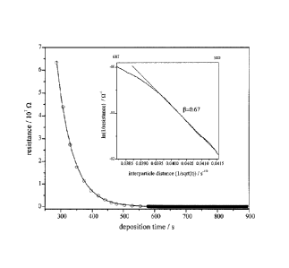
Figure 1 is a plot of resistance between two Ag electrodes on a polyethylene
(PE) film versus deposition time;
Figure 2 is a plot of resistance between two Ag electrodes on a PE film versus
time of exposure to CIEES;
Figure 3 is a plot of resistance across an Ag nanoparticle film as a function
of
exposure time to CIEES; and
4
CA 02663126 2009-04-16
Figures 4 and 5 are plots of absorbance of the Ag nanoparticle film as a
function of exposure time to CIEES and wavelength, respectively, the
absorbance
data being acquired simultaneously with the resistance data shown in Fig. 3.
DETAILED DESCRIPTION OF THE INVENTION
The inventors deposited nanoparticies on a substrate using a deposition
apparatus described elsewhere (see Pedersen, D.B. et al, J. Phys. Chem. C.,
111
(15), 5592-5598). Nanoparticles were first generated in the gas phase using a
magnetron DC-sputtering source. Application of a 280 V bias between an anode
cap
and a metal target caused a discharge in the 0.17 Torr pressure of Ar gas
maintained between them. The current flow to the discharge was kept to 200 mA.
Any Ar+ ions generated in the discharge were accelerated toward the negatively
biased metal target which they struck with force, thus liberating metal atoms
to the
gas phase. These atoms were swept up in the flow of Ar leaving the discharge
region. Upon leaving the sputtering region the atoms passed through an
aggregation zone where the collision frequency between metal atoms was high,
and
formation of nanoparticies occurred. The nanoparticies thus generated them
moved
downstream into the expansion zone, which was evacuated by a 500 L s' turbo
pump (Varian V-550). The nanoparticles then passed through an orifice into the
neighboring deposition chamber where a pressure of <10-4 Torr was maintained
during deposition by a 300 L s'1 turbo pump (Varian TV-301). The size of the
nanoparticles could be varied by varying parameters such as Ar and He gas flow
rates, aggregation zone length and discharging current. A substrate
(polyethylene or
glass) with painted silver electrodes positioned in front of the orifice
collected the
nanoparticles which deposited as 2D films of naked nanoparticles. The distance
between the particles varied with deposition time pseudo-continuously; at
longer
5
CA 02663126 2009-04-16
times more particles reside on the surface and the average interparticle
distance is
decreased accordingly. The resistance between electrodes was monitored during
deposition with an Agilent digital multimeter (34401A) connected to a computer
via
HPIB interface.
Exposure experiments were conducted in a fume hood. A nanoparticle-
coated polyethylene film was placed on a stand. Light exiting an optic fiber
connected to a halogen lamp passed through the sample and was collected by a
collimating lens attached to a second optic fiber, on the other side of the
sample, that
carried the light to the CCD array of a UV-vis spectrometer (Ocean Optics
SD2000).
In this configuration, the resistance between electrodes and the spectrum of
the
nanoparticies between electrodes could be monitored simultaneously during
exposure of the nanoparticle film to CIEES. Exposure was effected by opening a
bottle of CIEES (Aldrich, 98%) 5 cm from the film and letting the vapors
diffuse in the
fume hood.
The nanoparticle sensor was also exposed to sulfur mustard gas and HCN
warfare agent, and the sensor responded well to both. The sensor was exposed
to
CO and there was no response which demonstrates some selectivity.
The deposition of Ag nanoparticles generated by the sputtering source onto
substrates yielded two dimensional arrays of nanoparticles. A sample scanning
tunneling microscope (STM) image of a film deposited on highly ordered
pyrolitic
graphite (HOPG) revealed particles appearing as white shapes against a darker
background. The outline of each particle is discernible and the size easily
determined. From such images the 2D nature of the films was established and
the
diameter of the nanoparticles was found to be 2.8 0.5 nm. The distance
between
particles could be varied by varying the deposition time. The distance between
the
6
CA 02663126 2009-04-16
nanoparticles was found to be >10 nm but smaller interparticle separation was
possible by increasing the deposition time. In general, the interparticle
separation
has a well defined average value because the deposition is a random process.
It is
straightforward to show that a random deposition yields an average
interparticle
separation that varies inversely with tl'~, where t is the deposition time.
Accordingly,
plots of the interparticle distance versus the inverse of the square root of
the
deposition time are linear (see Pedersen et al supra). The linearity combined
with
STM data and trends in the optical properties of such films establish that the
films
are 2D arrays of nanoparticles with interparticle distances that decrease
steadily as
deposition time is increased.
For a 15 min deposition of Ag nanoparticies on a glass slide or polyethylene
film, the average interparticle distance is small enough that current can flow
between
two silver electrodes situated at either end of the nanoparticle film. When
the
particle density is low enough, such current is expected to flow via tunneling
of
electrons across the interparticle gaps. Controlling the distance between
adjacent
nanoparticles affords an opportunity to examine the distance dependence of the
through-space tunneling current between nanoparticles. A plot of the
resistance,
measured between two silver electrodes spaced 3 mm apart on the surface of a
polyethylene film, versus t is shown in Fig. 1. The resistance data were
obtained
between two Ag electrodes painted onto a 5 pm thick polyethylene film. The
electrodes were 3 mm apart. For each point in the early part of the
deposition, the
sputtering source was turned off so that the current flow associated with the
deposition of the 3.2 0.5 nm diameter Ag nanoparticle ions onto the
polyethylene
film did not affect the resistance measured. After 580 s, data were obtained
continuously with the source on because this effect was negligible. In the
inset, the
7
CA 02663126 2009-04-16
portion of the curve where In (resistance") versus the deposition time is
linear is
shown. A fit to the tunneling expression is shown as a solid, straight line.
These
data were collected in situ during deposition of the nanoparticles on the
polyethylene
surface. Similar results were obtained on glass. Early on in the deposition
the
resistance is infinite. As the particle density in the film increases it
eventually
reaches a critical value where a resistance and current flow is measurable.
The
average spacing between nanoparticles (i.e. outer edge to outer edge) at this
time is
6.0 0.5 nm, as determined by scanning tunneling microscopy (STM) imaging of
nanoparticies deposited on highly oriented pyrolytic graphite (HOPG) under
identical
conditions. At this distance, there is no direct, conducting path for
electrons to follow
and current flow occurs via tunneling of electrons between adjacent
nanoparticles.
As the distance between particles decreases further the tunneling rate
increases and
the resistance measured between electrodes decreases, as seen in Fig. 1.
The tunneling current, or rate of tunneling, is given by
1 =1oe"ad
where lo is the pre-exponential factor, d is the interparticle separation, and
9 is the
fall-off or attenuation factor. A fit of this equation to the inverse of the
resistance is
shown in the inset of Fig. 1. In the 26 - 150 k'S2 region the fit is good
indicating that
the tunneling distance between adjacent nanoparticles decreases steadily
during this
stage of the deposition. To establish a fit requires determining the
proportionality
factor A for d = At -y, which was done by measuring interparticle distance d
at
specific time t using STM imaging of Ag nanoparticies on HOPG. The value of A
obtained is expected to hold over a certain range of deposition times.
Accordingly,
the fit is good in the 26 - 150 k"f2 region but not elsewhere. From such fits
to a
number of data sets, the value of 13 obtained is 0.67 A-'. This value compares
well
8
CA 02663126 2009-04-16
with literature values that are typically 0.6 - 1.0 A"' (see Adams, D.M. et
al, J. phys.
Chem. B, 107 (28), 663-6997). The good comparison indicates that tunneling is
the
dominant mechanism of charge transport in the nanoparticle films with
comparable
interparticle separations.
The addition of molecules to the interparticle spaces is expected to change
the rate of tunneling and thus the resistance of the nanoparticle film. To
effect such
change, the nanoparticies were exposed to CIEES. A sample of the change in
film
resistance that resulted during the exposure is shown in Fig. 2. As seen,
within 1
min of opening a bottle of CIEES positioned 5 cm away, in a fume hood through
which air was flowing at a rate greater than 500 ft3 min-' with the electrodes
3 mm
apart, the resistance across the film had changed. Furthermore, the resistance
decreased from 6 MS2 to 160 kf2 within 8 min. The large change suggests high
sensitivity.
To gauge the sensitivity, the change in resistance and the change in the
optical properties of some nanoparticle films were monitored simultaneously.
Some
sample results of the optical and resistance data obtained are shown in Figs.
3 to 5.
Fig. 3 shows the resistance data across an Ag nanoparticle film. The
resistance
data were acquired simultaneously with the absorbance data shown in Figs. 4
and 5.
Lines A and B in Fig. 4 show changes in the absorbance measured at 700 and 650
nm, respectively as a function of exposure time t. In Fig. 5, the absorbance
spectrum is shown before (line C) and after (line D) the exposure.
Following exposure to CIEES, the resistance of the nanoparticle films
decreased significantly, as seen in Fig. 3, and stayed there. The effect was
irreversible. Heating of the films was not possible because the polyethylene
melts
and swells at relatively low temperatures, which would drastically alter the
9
CA 02663126 2009-04-16
interparticle spacing and conduction characteristics of the nanoparticle film.
Letting
the films off-gas by leaving the films to sit for several days had no effect;
CIEES
irreversibly adsorbed to the nanoparticies. In this context, the nanoparticle
films
function as cumulative sensors. Exposure of such sensors to trace amounts of
toxic
chemicals such as CIEES results in a steady build up of the toxic chemical on
the
surfaces of the nanoparticles. Eventually, the build up causes a change in
resistance large enough to be measured. The disadvantage of cumulative sensing
is
that the sensor is destroyed in the process. The advantage is that cumulative
sensors can detect trace quantities of toxic gas well below the detection
threshold of
concentration-based, one-time sampling techniques. Furthermore, the cumulative
sensor response changes steadily with time thus providing a continuous readout
related to the total amount of toxic chemical that the sensor has encountered
over
the total period of exposure. Accordingly, the sensor reading is directly
related to
concentration-time (CT) values used in determining the toxicity effect on
personnel
exposed to warfare agents and other toxic chemicals. In light of these sensing
properties and the highly portable nature of the nanoparticle films,
measurements of
resistance across these films is useful as a portable sensor platform suitable
for use
as personal exposure indicators and other related devices.
The method described above has been used to deposit copper nanoparticles
on an inert substrate, i.e. glass and polyethylene. Sensors can also be
produced
using any noble metal such as gold, platinum and palladium. The particle size
and
spacing of the nanoparticies are listed hereinbefore as 3.2 and 6.0,
respectively.
However, it has been determined that the particle size can be 1-100 nm and
preferably 2-50 nm, and the edge to edge spacing can be 4 to 50 nm and
preferably
5 to 25 nm.