Note: Descriptions are shown in the official language in which they were submitted.
CA 02663267 2009-03-12
WO 2008/033546 PCT/US2007/020081
IMPLANTABLE ELECTRODES WITH POLYOXOMETALATES
Technical Field
The present disclosure relates to biomaterials containing polyoxometalate
(POM) structures. More particularly, the disclosure relates to implantable
electrodes having POM structures.
Background
Implantable electrodes for electrical stimulation and sensing can be quite
small. One driving force for the reduction in electrode size is the increase
in
possible locations for implanting the electrode. In addition, the smaller
electrode
size also can lower stimulation thresholds and increase power supply (e.g.
battery) longevity. As can be appreciated, extending battery life allows for a
longer potential service life of the implanted device (e.g., pacemaker).
However,
with reduction of the size of the electrode (e.g., a reduction in the
geometric
surface area of the electrode) there is an increase in ctirrent density across
the
electrode. This increase in current density can increase the possibility to
exceed
safe electrical charge limits, which could result in electrode material
dissolution,
electrolyte redox reactions, and/or the production of toxic chemicals.
In an effort to control the current density various options have been
suggested and used to increase the actual electrode surface area without
increasing the overall physical -dimensions of the electrode. Examples of such
options include porous electrode materials, sintered microspheres, fractal
electrode surface morphology, and fractally coated electrodes. There, however,
continues to be a need for large actual electrode surface area while not
increasing
the overall physical dimensions of the electrode.
Summarv
Embodiments of the present disclosure provide for implantable
electrodes that include polyoxometalate (POM). In the various embodiments,
the POM may provide the implantable electrode with an electrochemically active
and flexible low polarization pseudo-capacitive electrode surface. Electrode
surfaces that include POM may be suitable for delivering low to high voltage
stimulation pulses, for example up to 10 volts, without exceeding a safe
charge
I
CA 02663267 2009-03-12
WO 2008/033546 PCT/US2007/020081
injection limit and electrochemical potential window. In addition, implantable
electrodes that include POM may also display reduced polarization losses at
the
electrode/tissue interface.
As used herein, "polyoxometalate" or "POM" includes metal-oxide or
metal-oxygen ions (e.g., anions), clusters or cages in their various forms,
including metal oxide cluster anions. In various embodiments, the POM may be
included in a film on the electrode surface. Alternatively, the POM may be
included as a doping ion in a polymer matrix to make an electrically active
polymer. In addition, the POM may help to increase the charge storage capacity
of the implantable electrode in which they are used due to POM redox
properties
(e.g., POM provides electroactive species with several oxidation states that
allow
for Faradaic redox transitions at the electrode/tissue interface). The pseudo-
capacitance property of the POM can include a combination of porosity, the
electro-active area (double layer) and Faradaic redox stages that POMs can go
through. As used herein, a "film" refers to a layer of an electrically
conductive
substance which is deposited, directly and/or indirectly, on a surface of an
implantable electrode.
Method embodiments for the present disclosure also include
incorporating the POM into a polymerizable mixture and forming a film of the
polymerizable mixture having the POM entrapped therein on the surface of the
electrode. Examples of such methods include, but are not limited to, chemical
or
electrochemical generation of the polymer from a solution where the POM is
present. The film formed during the electrochemical polymerization may
include homogeneously entrapping the POM in the film.
Other deposition techniques are also possible. For example, the film that
includes POM may be introduced into the film by an acid-base doping process
after the film is formed. As will be appreciated, other processes may also be
used to form the film, such as co-forming the film with the POM using a sol-
gel
process or other co-deposition process. Other deposition techniques include
adsorption, self-assembly through electrostatic interactions, layer-by-layer
deposition, and the Langmuir-Blodgett (LB) technique, among others.
The chemical composition and structures of the POM may also be
adjusted according to various embodiments to alter electrical performance of
the
film on the surface of the electrode. For example, selection and use of the
POM
2
CA 02663267 2009-03-12
WO 2008/033546 PCT/US2007/020081
and additional doping anions incorporated in the film can be used to control
the
capacitance and impedance of the resulting implantable electrode. The
electrode
surface may further be porous to allow for an additional increase in effective
surface area.
In addition to the POM acting as an electrical conductor, the film can
also be formed of a conductive polymer that is doped with the POM. Examples
of such conductive polymers include, but are not limited to, poly(pyrrole)s,
poly(thiophene)s, polynaphthalenes, poly(acetylene)s, poly(aniline)s,
poly(fluorene)s, polyphenylene, poly(p-phenylene sulfide), poly(para-phenylene
vinylene)s, and polyfurane.
Embodiments of the implantable electrodes having POM may be suitable
for use with wireless and wired electrodes. As used herein, an "electrode"
includes an electrically conductive structure (e.g., an electrode body) that
can be
used to provide and/or sense an electrical potential to and from biological
tissue.
Examples of such electrodes include, but are not limited to, electrodes used
for
sensing and pacing cardiac tissue (e.g., pacing electrodes), sensing and
delivering defibrillation energy to cardiac tissue (e:g., defibrillation
electrodes),
sensing electrical signals from and providing stimulation pulses to the
nervous
system including the brain, spinal cord, ear, and providing stimulation pulses
to
the vasculature system, to blood, and/or the urinary system. Such electrodes
can
have a coil configuration, a semi-hemispherical configuration, annular and/or
semi-annular ring electrodes, all with or without active anchoring mechanisms
(e.g., helical screw and/or tines).
In various embodiments, the electrode having the POM may be in the
form of a lead having a lead body, a conductor in the lead body, and the
electrode on the lead body having a surface that includes the POM. As
discussed
herein, the POM can be included in a film on the surface of the electrode. In
an
alternative embodiment, a wireless electrode may include a first and second
electrode having a surface with the POM and an induction coil coupled between
the first and the second electrode. The first and the second electrode may be
used to produce an electrical potential discharge from energy (e.g., radio
frequency energy) received with the induction coil. In addition, the wireless
electrode can further include a battery coupled to the induction coil, where
the
battery may be rechargeable with current generated from the induction coil
that
3
CA 02663267 2009-03-12
WO 2008/033546 PCT/US2007/020081
receives radio frequency energy from an external transmitter. The wireless
electrode may further include a storage capacitor coupled to the induction
coil to
store and deliver an electrical potential between the first electrode and the
second electrode.
Brief Description of the Drawings
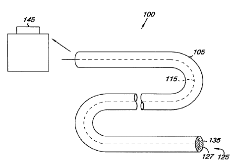
Figure 1 illustrates an embodiment of a lead having an electrode, where
the electrode has a film with a polyoxometalates (POM) according to the
present
disclosure.
Figure 2 illustrates an embodiment of a wireless electrode with
electrodes, where the electrodes have a film with POM according to the present
disclosure.
Figure 3 illustrates an additional embodiment of a wireless electrode with
electrodes, where the electrodes have a film with POM according to the present
disclosure.
Detailed Descrintion
The Figures herein follow a numbering convention in which the first
digit or digits correspond to the drawing Figure number and the remaining
digits
identify an element or component in the drawing. Similar elements or
components between different Figures may be identified by the use of similar
digits. For example, 110 may reference element "10" in Figure 1, and a similar
element may be referenced as 210 in Figure 2. It should also be apparent that
the
scaling on the figures does not represent precise dimensions of the various
elements illustrated therein.
The present disclosure provides for the incorporation of a metal oxide(s)
into an electrode surface, thereby forming a nanocomposite structure. In
particular, the present disclosure allows for polyoxometalates (POM), a class
of
metal oxide "clusters," or compounds, to be incorporated into an electrode
surface to allow for an increase in the electrochemically active and pseudo-
capacitive surface area of the electrode without increasing the overall
physical
dimensions of the electrode.
POM displays a similarity in redox properties to pseudo-capacitive
pacing electrodes such as iridium oxide (IrOx). Like IrOx, POM has the ability
4
CA 02663267 2009-03-12
WO 2008/033546 PCT/US2007/020081
to undergo a reversible multi-electrode redox process. POM can also provide
electroactive species with several oxidation states that allow for Faradaic
redox
transitions at an electrode/tissue interface. And like electrodes with IrOx,
electrodes having POM may have lower polarization, higher capacitances, lower
sensing impedance, and lower voltage thresholds.
According to the present disclosure, POMs may provide versatility in
terms of structural, electrochemical, and photophysical properties of the
resulting
electrode surfaces. Electrode surfaces having POM incorporated therein help to
reduce polarization losses of the electrode, while maintaining a satisfactory
potential window for electrical stimulation delivered using the electrode. POM
also displays good electrocatalytic activity in hydrogen peroxide and nitrogen
oxide reductions which is beneficial for electrode applications. Electrode
surfaces having the incorporated POM may also allow for charge transfer from
the electrode without a significant loss of energy.
Generally, POM compounds recited in the present disclosure can be
represented by the formula (I):
A,, [LiIvIR,J,Oy] (1)
where A is at least one ion selected from the group consisting of Group 1-17
(IUPAC) elements, sodium (Na), potassium (K), ammonium, alkyl ammonium,
alkyl phosphonium, and alkyl arsonium. L is at least one element selected from
the group consisting of hydrogen and Group 13-17 elements. M is at least one
metal selected from the group consisting of Group 4 and 7-12 metals. J is at
least one metal selected from the group consisting of Group 5-6 metals. The
subscript a is a number which when multiplied by the valence of A will balance
the charge on the POM complex within the brackets. The subscript 1 is a number
ranging from zero to about 20, the subscript m is a number ranging from zero
to
about 20, the subscript z is a number ranging from about 1 to about 50, and
the
subscript y is a number ranging from about 7 to about 150.
In one embodiment, L is at least one element of the group phosphorous
(P), arsenic (As), silicon (Si), aluminum (Al), hydrogen (H), germanium (Ge),
gallium (Ga), and boron (B); M is at least one element of the group zinc (Zn),
titanium (Ti), manganese (Mn), iron (Fe), cobalt (Co), nickel (Ni), rhodium
(Rh),
5
CA 02663267 2009-03-12
WO 2008/033546 PCT/US2007/020081
zirconium (Zr), iridium (Ir), ruthenium (Ru), copper (Cu), and rhenium (Re);
and
J is at least one metal of the group molybdenum (Mo), tungsten (W), chromium
(Cr), tantalum (Ta), and vanadium (V). In addition, subscript I ranges from
zero
to about 4; subscript m ranges from zero to about 6; subscript z ranges from
about 6 to about 24; and subscript y ranges from about 18 to about 80.
Examples of POM compounds include, but are not limited to
hexametalate anions [M,,,J6.,,,Oy], the Keggin anions [Li or2MmJ12.,,,Oy], and
the
Dawson anions [L2 to 4MmJ18_,,,Oy]. A specific example of a
heteropolyoxometalate is the compound H3PWr2040 which exhibits a typical
molecular structure of a Keggin anion. Other examples of
heteropolyoxometalates having the same structure include H4SiW12O40,
H3PMo12040, H5PMoioVZO40 and H4PMoiIV040. It is understood that these
examples are merely illustrative of heteropolyoxometalates and not intended to
be limitative of the class of heteropolyoxometalates.
According to embodiments of the present disclosure, POM may be
incorporated into the electrode surface. As discussed herein, this may be
accomplished by forming a film that includes the POM on the electrode surface.
The POM may then help to increase the electrochemically active surface area
and the capacitance of existing conductive electrode materials without having
to
increase the size of the implantable device. The increase in active surface
area
and capacitance may even allow for a reduction in physical size of the
implantable electrode, which would be beneficial in that it would promote ease
of delivery and reduced tissue trauma. The use of POM in the electrode surface
may also help to reduce polarization losses while remaining within a suitable
potential window for electrical stimulation.
According to the present disclosure, a variety of imniobilization
techniques may be useful in incorporating POM with the electrode. For
example, the POM may be bulk-entrapped in a polymer film that grows from a
solution containing dissolved monomer and the POM during a chemical or
electrochemical polymerization process. For example, during an
electrochemical polymerization process, the monomer may be electrochemically
oxidized at a polymerization potential giving rise to free radicals. These
radicals
can be adsorbed onto the electrode surface and subsequently undergo a wide
variety of reactions leading to the polymer network that, while forming,
entraps
6
CA 02663267 2009-03-12
WO 2008/033546 PCT/US2007/020081
the POM. As the polymerization occurs locally on the electrode surface the
POM would be entrapped in close proximity to the electrode surface. This is
particularly suitable for the coating of electrode surfaces.
Other polymerizable conditions are also possible. These can include
adsorption of the POM to the polymer film, chemical deposition, layer-by-layer
(LBL) self-assembly of the POM on the polymer film through electrostatic
interactions. Other LBL deposition techniques could also be used in
incorporating the POM into the polymer film. In addition, sol-gel processing
could be used to form films containing POM on electrodes. The Langmuir-
Blodgett (LB) technique could also be used to form films (e.g., lamellar
films) of
the POM on the polymer film.
Control over the composition, structure, thickness, functional properties
and orientation of a film that includes the POM can be influenced by the
deposition technique and the conditions under which the film is produced. For
example, the growth of a polymer film that includes the POM may depend on the
electrical character of the polymer. In addition, polymer film generated by
cycling the potential (e.g. potentiodynamically) or by generating at a fixed
potential (e.g. potentiostatically) may also allow for a more precise control
of the
film thickness and its growth.
As discussed herein, the POM may also be incorporated into an
implantable electrode by forming films of conductive polymers doped with POM
anions onto the electrode surface. As used herein, a conductive polymer may
include an organic polymer semiconductor that includes a band structure that
allows for eIectrical conductivity. Exemplary conductive polymers include, but
are not limited to, poly(pyrrole)s, poly(thiophene)s, polynaphthalenes,
poly(acetylene)s, poly(aniline)s (leuco-emeraldine-base, emeraldine-base, and
pernigraniline-base forms), poly(fluorene)s, polyphenylene, poly(p-phenylene
sulfide), poly(para-phenylene vinylene)s, polyfurane, and their derivatives.
The
film may, for example, be grown by electropolymerization.
Additional examples of conductive polymers and/or doping ions that may
be used with POM include those of a biological nature, those that display
supercapacitive properties, trans- and cis-polyacetylene, and/or polyvinyl
sulfonate (doping ion). For example, one embodiment of electrochemical
polymerization on a positive anode substrate is to mix solutions of pyrrole,
7
CA 02663267 2009-03-12
WO 2008/033546 PCT/US2007/020081
sodium polyvinyl sulfonate, and potassium polyoxymetalate and apply a
potential of 0.4 volts (V) to 1.2 V to the anode. The desired doping level of
the
potassium POM anions may then be adjusted with the polymeric dopant of
sodium polyvinyl sulfonate and/or polystyrene sulfonate. In one embodiment
the POM is an isopoly anion of the form [M,,,Oy]p- or a heteropoly anion of
the
form [MmJ,O']Q" where M and J are as described herein.
Films of conductive polymers may also be formed by a Iayer-by-layer
(LBL) self-assembly process which enables a layer-by-layer growth of films and
the control of the composition, thickness, and orientation of each layer at
the
molecular level. As discussed, the LBL assembly process includes alternate
adsorption of oppositely charged species via electrostatic attraction that can
produce thin multilayer film structures. Also, the LBL self-assembly process
can be used with POMs and diazoresin. In this case, the POM complexes with
the diazopolymer were the usual ionic bonds formed between the compounds
may be switched into covalent bonds, making a very stable thin film useful for
long term applications in the body.
By way of example, multilayer films that include POM can by formed by
the LBL process generally through a series of coating steps in aqueous
solutions.
During the coating steps, an electrode substrate can be dipped into a cationic
aqueous solution containing a conductive polymer (e.g., polyaniline) and then
into an anionic aqueous solution containing a POM. Molar concentrations of the
solutions can be small (e.g. 0.1M, 0.01M or 0.001M) with an acidic pH (e.g.,
less than about pH=5). Such multilayer films can be formed by alternately
immersing the desired electrode surface into the solutions of the cationic
conductive polymer and the anionic POM for a predetermined time with
intermediate water washing and drying.
In a further embodiment, POM may be incorporated at the electrode
surface after polymerization of the film by acid-base doping. For example, the
electrode surface can be made basic by the physical adsorption of a base, or
chemical modification of the electrode surface with a base. A POM anion can
then be introduced to the basic activated electrode surface to react with the
base
so as to form an adsorbed ion pair comprising POM anion and the protonated
base. There may also be direct coordination by a donor atom to a peripheral
8
CA 02663267 2009-03-12
WO 2008/033546 PCT/US2007/020081
heteroatom in a POM compound that possesses an-open site or a weakly.bound
exchangeable ligand.
In additional embodiments, the concentration of POM anions in the
electrode surface can be adjusted by co-incorporation of other doping anions.
Other doping anions can be selected from the group consisting of biomolecules,
including, but not limited to, tripolyphosphate, citrate, cyanate groups,
heparin,
or sulphate groups, for example. Use of the additional doping anions with the
POM anions can allow for the electrode capacitance and impedance to be
controlled and tailored by varying the chemical composition and doping level
of
the POM anions.
The electrode surfaces of the present disclosure can also have different
physical configurations. For example, the electrode surfaces for receiving the
conductive film can be porous, sintered, and/or patterned. Examples of
suitable
porous electrode surfaces include those materials selected from the group of
platinum (Pt) and conductive ceramics such as iridium oxide, tungsten carbide,
silicone carbide, titanium oxide-iridium oxide (Ti0z-IrO2), iridium oxide -
tantalum dioxide (Ir02-Ta02), tin oxide, indium oxide, and fullerene. These
materials can be made porous by sputtering, electrodeposition, or sol-gel
processes. On the other hand, the porous electrode surfaces can also be co-
formed with POM anions using a process selected from the group of sol-gel
processes, various methods of co-depositing (layer-by-layer self-assembly),
and
reactions with pendant surface ligands.
Additional electrode surfaces useful with the present disclosure include,
but are not limited to, activated carbon, carbon aerogels, carbon foams
derived
from polymers, oxides, hydrous oxides, nitride ceramics such as TiN, carbides,
nitrides and other conducting polymers. Examples of oxides and hydrous oxides
include Ru02, IrOa, NiO, Mn02, VO,,, Pb02 and Ag20. Also, examples =of
carbides and nitrides include MoQ,, MOaN, WC x and WNc.
As discussed herein, immobilized POM anions in the electrode surface
can increase the number of conductive surface sites and the capacitance of the
resulting electrode. For example, by adjusting the chemical composition of the
POM anions structure (e.g., various combinations of ternary and binary mixed
oxide combinations) the capacitance, polarization, electrochemical
performance,
and stability of the resulting electrode can be modified. Also, providing a
larger
9
CA 02663267 2009-03-12
WO 2008/033546 PCT/US2007/020081
surface area for the electrode through the use of the POM anions as described
herein can decrease the current density and increase capacitance, all while
the
geometric surface area of the electrode remains substantially unchanged.
Besides providing for a larger surface area, POM can also provide a
combination
of porosity, the electro-active area (double layer) and Faradaic redox stages
that
POMs can go through, as discussed herein.
Examples of such electrodes include, but are not limited to, electrodes
used for sensing and pacing cardiac tissue, sensing and delivering
defibrillation
energy to cardiac tissue, sensing electrical signals from and/or providing
stimulation pulses to the cells of the nervous and neurological system
including
the brain, spinal cord, ear, and providing stimulation pulses to the
vasculature
system, to blood, and/or the urinary system.
Embodiments of the electrode surfaces having the POM can be used with
lead electrodes and/or with wireless electrodes. In various embodiments, the
lead electrodes having the POM include a lead body, a conductor in the lead
body, and an electrode on the lead body having a surface with the POM. In an
alternative embodiment, the wireless electrode has a first and second
electrode
having a surface with the POM and an induction coil coupled between the first
and the second electrode. The first and the second electrode can produce an
electrical potential discharge from radio frequency energy received with the
induction coil. In addition, the wireless electrode can further include a
battery
coupled to the induction coil, where the battery is rechargeable with current
generated from the induction coil that receives radio frequency energy from an
extemal transmitter. The wireless electrode can further include a storage
capacitor coupled to the induction coil to store and deliver an electrical
potential
between the first electrode and the second electrode.
Figure 1 provides an illustration of a lead 100. As shown, the lead 100
includes a lead body 105 with a conductor 115 in the lead body 105. The
conductor 115 is shown coupled to an electrode 125 having surface 127. A pulse
generator (e.g., a pacemaker) 145 is also shown, where the lead 100 can be
releasably attached to the pulse generator 145 via a header structure. In one
embodiment, the pulse generator 145 can include electronic components to
perform signal analysis, processing and control. Such electronic components
can include one or more microprocessors to provide processing and evaluation
of
CA 02663267 2009-03-12
WO 2008/033546 PCT/US2007/020081
sensed cardiac signals to determine and control delivery of electrical shocks
and/or pulses of different energy levels and timing for ventricular
fibrillation,
atrial fibrillation, cardioversion, and/or pacing (dual or single chamber) to
the
heart in response to cardiac arrhythmias including fibrillation, tachycardia
and
bradycardia. The pulse generator 145 can also include a power supply, such a
battery, a capacitor(s), and other components.
According to the present disclosure, the surface 127 of electrode 125
includes a film 135 having the POM formed according the embodiments of the
present disclosure. Examples of materials for the electrode 125 are also
according the embodiments of the present disclosure discussed herein. For
example, material for the electrode 125 can include, but is not limited to,
platinum (Pt), gold (Au), and iridium (Ir).
In an additional embodiment, the conductor 115 in the lead body 105 can
also be formed, at least partially, from a polymer doped with the POM anions
according to the present disclosure. For this embodiment, the polymer doped
with the POM anions can be deposited, cast or extruded to form the conductor
115. In addition, it would be possible to co-extrude the POM anions doped
polymer forming the conductor 115 with the surrounding lead body 105.
Material selection for the lead body 105 can be from materials known in the
art.
In a further embodiment, the lead 100 can be configured to be
biodegradable. For example, the conductor 115 can be formed from deposited
layers of POM around which is formed a lead body 105 of a biodegradable
polymer. One way to form the biodegradable conductor 115 is to use the LBL
self-assembly approach, creating layers of anionic POM with any suitable
cationic counter molecule. For example, chitosan layers incorporated with POM
can form ionic bonds between the layers, which can be slowly eroded by various
salt ions in the body. Further examples of biodegradable polymers can include,
but are not limited to, polycarboxylic acid, polyanhydrides including maleic
anhydride polymers; polyorthoesters; poly-amino acids; polyethylene oxide;
polyphosphazenes; polyactic acid, polyglycolic acid and copolymers and
copolymers and mixtures thereof such as poly(L-lactic acid) (PLLA), poly (D,L,-
lactide), poly(lactic acid-co-glycolic acid), 50/50 (DL-lactide-co-glycolide);
polydioxanone; polypropylene fumarate; polydepsipeptides; polycaprolactone
and co-polymers and mixtures thereof such as poly(D,L-lactide-co-caprolactone)
11
CA 02663267 2009-03-12
WO 2008/033546 PCT/US2007/020081
and polycaprolactone co-butylacrylate; polyhydroxybutyrate valerate and
blends;
polycarbonates such as tyrosine-derived polycarbonates and arylates,
polyiminocaronates, and polydimethyl-trimethylcarbonates; cyanoacrylate;
calcium phosphates; polyglycosaminoglycans; macromolecules such as
polysaccharides (including hyaluronic acid, cellulose, and hydroxypropylmethyl
cellulose; gelatin; starches; dextrans; alginates and. derivatives thereof),
proteins
and polypeptides; and mixtures and copolymers of any of the foregoing. The
biodegradable polymer may also be a surface erodable polymer such as
polyhydroxybutyrate and its copolymers, polycaprolactone, polyanhydrides
(both crystalline and amorphous), and maleic anhydride copolymers.
In addition, the electrode 125, including the film 135 can be also be
formed of a biodegradable conductive polymer doped with POM anions formed
thereon according to the present disclosure. In this embodiment, the electrode
125 can be formed of a material prone to oxidation, such as iron (Fe) and/or
magnesium (Mg).
Figure 2 provides an illustration of a wireless electrode 210 according to
the present disclosure. The wireless electrode 210 includes a first electrode
220
and a second electrode 240, with an induction coil 250 coupled between the
electrodes 220, 240. One or both of the surfaces of the first and second
electrodes 220, 240 can further include the film 235 having the POM according
to the present disclosure. The induction coil 250 receives energy 260 that
intersects the induction coil 250 at a parallel angle to produce an electrical
potential discharge between the electrodes 220, 240.
In yet another embodiment, the wireless electrode 210 can be configured
to be biodegradable. For example, the induction coil 230 can be made by
building up layers of POM then insulating the POM with a biodegradable
polymer insulator sheath. In addition, the electrodes 220 and 240 can be
formed
from one or more biodegradable polymers and/or the oxidizing metals, as
discussed herein.
Figure 3 provides an additional embodiment of the wireless electrode 310
that further includes a battery 370 and a storage capacitor 380 coupled to the
induction coil 350 as well as an f1C/DC converter (not shown). The battery 370
is rechargeable with current generated from the induction coi1250 from
received
RF energy 360 from an external transmitter. The storage capacitor 380 coupled
12
CA 02663267 2009-03-12
WO 2008/033546 PCT/US2007/020081
to the induction coil 350 can then be used to store and deliver an electrical
potential between the first electrode 320 and the second electrode 340.
Examples of such wireless electrodes are provided in a commonly assigned U.S.
Patent Application entitled "Leadless Cardiac Stimulation System" (BSCI
Docket #04-0229), which is incorporated herein by reference in its entirety.
An additional embodiment of the present disclosure is to provide
electrical stimulation to the surface of an implanted medical device having
the
POM anions to enhance healing of the surrounding tissues. For example,
electrode surfaces having the POM anions as discussed herein can be integrated
into surfaces of implants such as vascular grafts, synthetic heart valves, and
left
ventricular assist device (LVAD) surfaces where stimulation pulses are
delivered
to tissues adjacent the implant by an implanted or remote energy source. The
voltage amplitude of the pulses must be adequate to stimulate cells, yet be
below
the threshold for noxious reactions at the electrode surface. This may be
achieved in part by applying the films containing the POM to the electrodes
that
increase the electrode surface area without increasing the geometric surface
area
of the implant as described in the embodiments herein. Examples of such
medical devices are provided in a commonly assigned U.S. Patent Application
entitled "Stimulation of Cell Growth at Implant Surfaces " (BSCI Docket #04-
0062), which is incorporated herein by reference in its entirety.
The invention has been described with reference to various specific
embodiments and described by reference to examples. It is understood,
however, that there are many extensions, variations, and modification on the
basic theme of the present invention beyond that shown in the examples and
detailed description, which are within the spirit and scope of the present
invention.
The complete disclosures of the patents, patent documents, and
publications cited herein are incorporated by reference in their entirety as
if each
were individually incorporated. Various modifications and alterations to this
disclosure will become apparent to those skilled in the art without departing
from the scope and spirit of this disclosure. It should be understood that
this
disclosure is not intended to be unduly limited by the illustrative
embodiments
and examples set forth herein and that such examples and embodiments are
13
CA 02663267 2009-03-12
WO 2008/033546 PCT/US2007/020081
presented by way of example only with the scope of the disclosure intended to
be limited only by the claims set forth herein as follows.
In the foregoing Detailed Description, various features are grouped
together in several embodiments for the purpose of streamlining the
disclosure.
This method of disclosure is not to be interpreted as reflecting an intention
that
the embodiments of the disclosure require more features than are expressly
recited in each claim. Rather, as the following claims reflect, inventive
subject
matter lies in less than all features of a single disclosed embodiment. Thus,
the
following claims are hereby incorporated into the Detailed Description, with
each claim standing on its own as a separate embodiment.
14