Note: Descriptions are shown in the official language in which they were submitted.
CA 02664502 2009-04-28
TITLE: TRANSCEIVER ARCHITECTURE
FIELD OF THE INVENTION
[0001] The present invention relates to wireless data equipment, and more
particularly to radio modems that operate across a wide range of frequency
bands, for
example, license and/or free frequency bands.
BACKGROUND OF THE INVENTION
[0002] In the art, there are radio modems with known receiver architectures
for
demodulating a signal.
[0003] Superheterdyne double conversion receivers are a known architecture and
deliver adequate performance. Such receivers, however, are expensive and are
only able
to receive signals in a narrow frequency range, for example, when good RF
blocking
(interference immunity) and phase noise performance are required. Transmitters
known
in the art also have a limited frequency range of operation in order to
achieve good phase
noise performance and to meet tight regulatory emission masks (e.g. FCC Part
90). In
order to cover a wide frequency range (i.e. different frequencies of
operation), a
manufacturer needs to make and support numerous models of superheterdyne
double
conversion receivers.
[0004] Low and zero intermediate frequency (IF) receivers are also known in
the
art but suffer from different limitations. These receivers suffer from low
interference
blocking and/or lower adjacent channel rejection which allows unwanted signals
to
contaminate the desired passband signal. The rejection of the interfering
signal can be
optimized by calibrating the in-phase (I) and quadrature (Q) receiver
components,
however, the calibration process increases installation and production costs.
Furthermore, to achieve a high dynamic frequency range the receivers typically
use
higher order analog to digital conversion circuits, which further increases
the cost and/or
power consumption of the circuit.
CA 02664502 2009-04-28
-2-
[0005] In view of at least these deficiencies, a need remains in the art for
improvements in radio modem and wireless communication systems design.
BRIEF SUMMARY OF THE INVENTION
[0006] The present invention comprises embodiments of a transceiver
architecture and embodiments for an improved radio modem.
[0007] According to a first aspect, there is provided a radio modem
comprising: a
transmitter module and a receiver module; a transducer, the transducer having
an input
port coupled to said transmitter module and an output port coupled to the
receiver
module; the receiver module including a receiver stage having an input port
coupled to
the output port of the transducer and including a receiver stage output port,
an
intermediate frequency stage having an input port coupled to the receiver
stage output
port and including an intermediate frequency stage output port, a channel
selection stage
having an input port coupled to the intermediate frequency stage output port,
and a
demodulation and output stage having an input port coupled to the intermediate
frequency stage output port; and the transmitter module including a transmit
signal
modulation stage and a transmitter stage, the transmit signal modulation stage
having an
input port for receiving a transmit signal input and being configured to
generate a
transmit signal output on an output port coupled to the transmitter stage, and
the
transmitter stage having a transmit signal output port coupled to the input
port of the
transducer.
[0008] According to another aspect, there is provided a receiver module for a
communication device, the receiver module comprises: a receiver stage having
an input
port for receiving a receive signal from a transducer and a receiver stage
output port; an
intermediate frequency stage having an input port coupled to the receiver
stage output
port and including an intermediate frequency stage output port; a channel
selection stage
having an input port coupled to the intermediate frequency stage output port
and
including a channel selection stage output port; a demodulation and output
stage having
CA 02664502 2009-04-28
-3-
an input port coupled to the channel selection stage output port and an output
port for a
receive output signal and the intermediate frequency stage is configured to at
least
partially down-convert a receive input signal from the receiver stage to
produce a receive
signal having a lower frequency, and the intermediate frequency stage is
configured to be
responsive to one or more control signals generated by a controller.
[0009] According to another aspect, there is provided a transmitter module
suitable for a communication device, and the transmitter module comprises: a
transmit
signal modulation stage, the transmit signal modulation stage having an input
port for
receiving a transmit signal input and being configured to generate a transmit
signal output
on an output port; and a transmitter stage having an input port coupled to the
output port
of the transmit signal modulation stage, and being configured to generate a
transmit
signal on an output port coupled to the input port of the transducer.
[00010] Other aspects and features of the present invention will become
apparent
to those ordinarily skilled in the art upon review of the following
description of
embodiments of the invention in conjunction with the accompanying figures.
BRIEF DESCRIPTION OF THE DRAWINGS
[00011] Reference is made to the accompanying drawings which show, by way of
example, embodiments of the present invention, and in which:
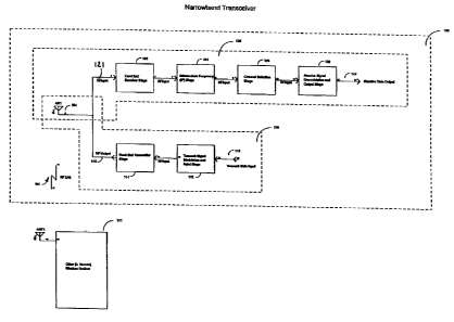
[00012] Fig. 1 shows in block diagram form a radio modem according to an
embodiment of the present invention;
[00013] Fig. 2 shows in schematic form a receiver circuit for the radio modem
according to an embodiment; and
[00014] Fig. 3 shows in schematic form a transmitter circuit for the radio
modem
according to an embodiment.
CA 02664502 2009-04-28
-4-
[00015] In the drawings, like references indicate like elements or components.
DETAILED DESCRIPTION OF AN EMBODIMENT
[00016] Reference is made to Fig. 1, which shows in block diagram form a radio
modem according to an embodiment of the present invention and indicated
generally by
reference 100. The radio modem 100 as described is suitable to either a
license
frequency band or a free frequency band environment or application. It will be
appreciated that the invention or aspects of the invention may be applicable
to other types
of radio modems or wireless communication applications.
[00017] As depicted in Fig. 1, the radio modem 100 provides a communication
(e.g. wireless) link 102, comprising a transmit channel and/or a receive
channel, for
sending to and/or receiving information from other radio or wireless devices,
indicated
generally by reference 101. The other device 101 includes, for example, a
radio modem,
a wireless network router, and a wireless handheld communication device such
as a
cellular phone or a BlackberryTM device. The channels in the communication
link 102 are
implemented utilizing optical communication or radio communication techniques.
[00018] As depicted in Fig. 1, the radio modem 100 includes a transducer 104,
for
example, a radio antenna. The radio modem 100 comprises a transmitter circuit
110 and
a receiver circuit 120. In one exemplary implementation, the transmitter
circuit 110
comprises a transmit data input and modulation stage 112, and a transmitter
front-end
stage 114. In known manner, the transmitter circuit 110 is configured to
convert transmit
information, e.g. digital data, applied at a transmit data input 111 into a
wireless (e.g.
FM) signal, which is transmitted by the antenna 104.
[00019] Referring to Fig. 1, the receiver 120 comprises a front-end receiver
stage
or module 122, an intermediate frequency (IF) stage 124, a channel selection
stage 126,
and a receive signal demodulation and output stage 128. The front-end receiver
stage
122 inputs a radio signal 121 (e.g. from the receive channel in the
communication link
CA 02664502 2009-04-28
-5-
102) from the antenna 104 which converts the wireless signal to the radio
signal 121.
The intermediate frequency (IF) stage 124 down-converts (for example,
partially) the
signal, as will be described in more detail below with reference to Fig. 2.
The channel
selection stage 126 is configured to allow input signals within a certain
(e.g. "tuned")
frequency range to continue to the receive signal demodulation and output
stage 128.
The receive signal demodulation and output stage 128 is configured to receive
the output
from the channel selection stage 126 and convert (e.g. demodulate) the signal
into receive
data (e.g. digital data stream). The digital stream data is outputted at a
receive data output
129 for further processing by an electronic device, for example, a mobile
communication
device or a computer, and/or an application program (e.g. web browser), for
example, as
indicated generally by reference 103 in Fig. 3.
[00020] According to an embodiment, the functionality associated with the
receive
signal demodulation and output stage 128 of the receiver 120 and the transmit
signal
modulation and input stage 112 of the transmitter 110 is implemented and
performed in
one component or module, for example, a narrowband transceiver, such as Analog
Devices ADF7021 transceiver device). According to an embodiment, a
microprocessor
(for example, as shown in Figs. 2 and 3 and is indicated generally by
reference 280) is
configured (for example, under stored program control) to control whether the
radio
modem is operating in "transmit mode" or "receive mode" as will be within the
understanding of one skilled in the art. To transmit information, the
microprocessor 280
(for example, as shown in Fig. 3) is configured (e.g. operates or executes
instructions in
firmware and/or software) to actuate an antenna switch 214 (Fig. 3) to close
the transmit
circuit 110 and allow the RF output signal 115 to continue to its intended
destination via
the RF link 102, as described in more detail below with reference to Fig. 3.
To receive
information, the microprocessor (for example, as shown in Fig. 2) is
configured to
execute instructions (for example, in firmware and/or software) to actuate the
antenna
switch 214 (Fig. 2) to close the receive circuit 120 and allow the RF input
signal 121 that
is received via the communication link 102 to continue along the receive
circuit 120, as
described in more detail below with reference to Fig. 2.
CA 02664502 2009-04-28
-6-
[00021] Reference is next made to Fig. 2 which shows in schematic form an
embodiment of the receiver channel module or circuit, which is indicated
generally by
reference 200. According to an embodiment, the receiver channel circuit 200 is
configured to partially convert, i.e. "down-convert", a receive signal 202
(i.e. the RF
input signal 121 in Fig. 1) from the antenna 104 into a lower or intermediate
frequency
(IF) signal, which is then subjected to further processing as described in
more detail
below. According to an embodiment and as shown in Fig. 2, the receiver channel
circuit
200 comprises a front end receiver stage 210, an intermediate frequency (IF)
mixer stage
220, and a receive signal demodulation and output stage 260. According to an
embodiment, the receiver channel circuit 200 includes a channel selection
stage indicated
generally by reference 240 in Fig. 2. According to another aspect, the
receiver channel
circuit 200 includes microprocessor 280. The microprocessor 280 operates under
stored
program control, for example, software or firmware stored in non-volatile or
program
memory and indicated generally by reference 282, and is configured to execute
instructions in the firmware 282 to provide the functionality and operations
associated
with the receiver, as described in more detail below.
[00022] As shown in Fig. 2, the front-end receiver stage 210 includes a pre-
scalar
filter 212, an antenna switch 214, a low noise amplifier (LNA) 216, and a
bandpass filter
218. The intermediate frequency (IF) stage 220 includes an IF mixer 222 and a
frequency
synthesizer component or device 224. The IF mixer 222 is configured to receive
an input
from the bandpass filter 218 and another input from the frequency synthesizer
224. The
channel selection stage 240 includes a channel selector 242 and an
intermediate
frequency (IF) amplifier 244. The receive signal demodulation and output stage
260
comprises a narrowband transceiver, indicated generally by reference 262.
[00023] Referring again to Fig. 2, the receive signal (i.e. RF input signal
121 in
Fig. 1) 202 is fed into the pre-scalar filter 212 which has a low noise figure
(for example,
in the range of 0.5 dB to 1.5 dB). The pre-scalar filter 212 may be
implemented using
various technologies, such as, helical, ceramic, a tuned LC network, micro-
strip, cavity or
waveguides, as will be within the understanding of one skilled in the art.
According to
I
CA 02664502 2009-04-28
-7-
another aspect, the pre-scalar filter 212 provides a filtering function and
depending on the
radio architecture is configured as a lowpass, bandpass, highpass or bandstop
filter. The
output of the pre-scalar filter 212 is fed to the antenna switch 214 and
switched or routed
(for example, under control of the microprocessor 280, i.e. executing an
algorithm or
instructions in software or firmware 282) to an output 215 which is coupled to
the input
of the low noise amplifier 216. The low noise amplifier 216 is configured to
amplify the
output signal from the pre-scalar filter 212, while introducing minimum noise
figure (e.g.
in the range of 0.5 dB to 1 dB). According to an embodiment, the low noise
amplifier 216
is configured or implemented to provide a gain in the range of 14 to 20 dB.
The amplified
output signal from the low noise amplifier 216 is next passed through the
bandpass filter
218. According to an embodiment, the bandpass filter 218 is implemented with a
passband or bandwidth of the entire desired frequency operating range (e.g.
400 MHz
to 480 MHz).
[00024] As shown in Fig. 2, the output from the bandpass filter 218 is fed to
one
input of the IF mixer 222. The IF mixer 222 has another input which receives a
frequency
signal which is generated by a frequency synthesizer indicated generally by
reference
224. According to an embodiment, the frequency synthesizer 224 generates an IF
frequency signal (i.e. local oscillator or LO signal) 221 having a frequency,
for example,
in the range 70 MHz to 150 MHz. The IF mixer 222 is configured to mix the
signal from
frequency synthesizer 224 with the signal from the bandpass filter 218 to
produce a lower
intermediate frequency (IF) signal 223 at the output of the IF mixer 222.
According to an
embodiment, the Frequency Synthesizer 224 is configured to be responsive, e.g.
tunable
with high resolution (e.g. 100 Hz), in response to one or more control signals
generated
by the microprocessor 280. According to an embodiment, the firmware 282
includes one
or more algorithms, functions, objects or code components configured to
program the
operational or desired receive frequency of the radio modem using a serial
peripheral
interface (SPI) port. The programming sequence of the frequency synthesizer
224 will be
defined by the manufacture of the device as will be within the understanding
of one
skilled in the art. According to another embodiment, the function(s) performed
by the
CA 02664502 2009-04-28
-8-
microprocessor 280 and/or firmware 282 may be implemented in hardware, in a
programmable or configurable hardware device and/or a hardware/software
combination.
[00025] According to an embodiment of the present invention, the frequency
synthesizer 224 is implemented with a plurality of tuning elements and the
tuning
elements are configured to be selectable in response to control signals
generated by the
microprocessor 280 in order to generate a local oscillator (LO) signal 221
having a
desired frequency for input to the IF mixer 222. According to an aspect, the
receiver 200
is configurable for operation over a wide frequency range by controlling or
setting the
local oscillator (LO) signal 221 to the IF mixer 222 with the frequency
synthesizer 224.
In a typical application, the RF frequency signal (i.e. the local oscillator
signal 221)
generated by the Frequency Synthesizer 224 and applied as the second input to
the IF
mixer 210 is in the range of 300 MHz to 420 MHz.
[00026] According to an embodiment of the present invention, the
software/firmware 282 is configured to re-program or reconfigure the local
oscillator
(LO) signal 221 while the radio modem is operational in the field without
interruption to
the communication link. In such a case, the radio modem can be modified to
receive
signals in a different frequency band. According to an embodiment, the
software/firmware 282 is configured to allow the receiver 200 to receive
multiple
channels of wireless information by programming or configuring the frequency
registers
inside the frequency synthesizer 224, as will be within the understanding of
one skilled in
the art.
[00027] Referring again to Fig. 2, the mixed output signal 223 generated by
the IF
mixer 222 is fed into the channel selection stage 240. As described above, the
channel
selection stage 240 comprises the channel selector 242 and the intermediate
frequency
(IF) amplifier 244. According to an embodiment, the channel selector 242 is
implemented
in the form of a highly selective bandpass filter that allows signals in a
narrow frequency
range or passband to continue along the receiver circuit. For example, the
channel
selector 242 may comprise a crystal, saw, baw, helical, lumped element or
quartz filter or
CA 02664502 2009-04-28
-9-
any other suitable device. According to an embodiment, the passband frequency
range is
typically in the range 12 kHz to 30 kHz with a center frequency from 70 MHz to
150
MHz. The channel selector 242 prevents signals that are outside of the desired
frequency
range from continuing along the path of the circuit, for example, by
sufficiently
attenuating them to be effectively negligible. As shown, the output from the
channel
selector 242 is fed into the intermediate frequency (IF) amplifier 244.
According to an
embodiment, the IF amplifier 244 is configured to amplify the signal with a
gain in the
range of 10dB to 20dB.
[00028] As depicted in Fig. 2, the output from the intermediate frequency (IF)
amplifier 244 is fed into the narrowband transceiver 262 in the receive signal
demodulation and output stage 260, after the noise and undesired signals are
removed by
the channel selector 242. The narrowband transceiver 262 is configured or
controlled by
the microprocessor 280 (i.e. under stored program control) to provide a
constant IF
frequency (e.g. 90 MHz), and demodulation bandwidth (e.g. 18.5 kHz) and signal
type (2
level FSK) in order to demodulate/convert the processed receive signal into
receive data,
for example, in the form of a digital data stream. The narrowband transceiver
262
receives the desired signal at the IF frequency. As described above and
according to an
embodiment, the IF frequency is substantially constant. According to another
aspect, the
IF frequency is not changed, i.e. re-tuned, on a channel-by-channel basis, but
is rather
tuned through the frequency synthesizer 224. According to an embodiment, the
microprocessor 280 executes an algorithm or function (in firmware or software
282) to
generate control signals 265a and 265b and actuate switches 267 which
activate/deactivate inductors 263a and 263b coupled to the oscillator 261. The
inductors
are configured to modify the tuning range of the narrowband transceiver in
order to
support the required IF frequency for demodulation. According to an
embodiment, the
microprocessor will not actuate 265a or 265b in order to achieve the IF tuning
range in
receive mode (e.g. 90 MHz).
[00029] The output of the narrowband transceiver 262 is coupled to an input
port
on the microprocessor 280. The firmware 282 executed by the microprocessor 280
CA 02664502 2009-04-28
-10-
includes a function, object or other type of code component, which is executed
to convert
or "re-package" the digital data stream into a format that can be understood
by other types
digital devices (e.g. a bit stream is re-packaged into groups of 8 bits to
represent a byte of
data). The re-packaged digital stream is outputted by the microprocessor 280,
i.e. as a
digital data output 284, to the digital device, for example, a mobile
communication
device or a computer 103 (Fig. 3).
[00030] Reference is next made to Fig. 3 which shows in schematic form an
embodiment of the transmitter channel module or circuit, which is indicated
generally by
reference 300. The transmitter channel circuit 300 comprises a transmit data
input and
modulation stage 310 and a front end transmission stage 320.
[00031] As shown, the transmit data input and modulation stage 310 comprises a
narrowband transceiver 312. According to an embodiment, narrowband transceiver
312
corresponds to the narrowband transceiver 262 of Fig. 2, and is configured to
directly
modulate a transmit input signal 311 across a wide frequency range. The
narrowband
transceiver 312 includes a local oscillator or LO (indicated generally by
reference 314).
According to an embodiment, the oscillator 314 is configured to be responsive
to control
signals generated by the microprocessor 280 operating under stored program
control, e.g.
a function or code component in the firmware 282. According to an embodiment,
the
microprocessor 280 executes an algorithm or instructions in firmware or
software 282 to
program or configure the local oscillator (LO) 314 to the desired frequency
for
transmission.
[00032] According to an embodiment, the local oscillator 314 is referenced
from
the maximum allowable input clock rate in order to achieve the best phase
noise
performance to meet regulatory emission mask (e.g. FCC Part 90 emission mask
D)
[00033] According to an embodiment, the microprocessor 280 executes a function
or instructions in firmware or software 282 to generate control signals on
outputs 316a,
316b and 316c, for example, using a serial peripheral interface or SPI. The
control signals
CA 02664502 2009-04-28
-11-
316a to 316c (e.g. the control signals may be data, clock and chip select)
according to an
embodiment configure the narrowband transceiver 312 into transmit mode and set
the
modulation characteristics and the transmission frequency. According to an
embodiment,
the narrowband transceiver 312 is implemented using an ADF7021 device from
Analog
Devices and includes registers for configuring the operation and/or functions
associated
with the device. The particular settings/configurations are detailed in the
device datasheet
and will be within the understanding of one skilled in the art. According to
an
embodiment, the microprocessor 280 generates control signals 317a and 317b to
actuate
diode switches 318, which activate/deactivate inductors 319 coupled to the
oscillator 314.
The inductors are configured to extend the tuning range of the narrowband
transceiver
312 by changing the resonating frequency range of the oscillator 314, and
thereby the
transmitter 300 to a specific transmit frequency, for example, in the range
350 MHz to
390 MHz when 317a is actuated and 317b is not actuated and 390 MHz to 430 MHz
when 317a is not actuated and 317b is actuated.
[00034] According to another aspect, the software/firmware 282 or selected
code
modules or functions are configurable locally, remotely, or autonomously to
send various
control signals to the narrowband transceiver 312 so that the radio uses
different
frequencies over a given time period (for example frequency hopping). This
allows a user
to adjust the transmit frequency of the radio modem 100, for example, even
while the
radio modem is operational in a field environment and without user
intervention.
[00035] The narrowband transceiver 312 is configured to perform direct
modulation of the RF transmit input signal 311. According to an embodiment,
the
narrowband transceiver also demodulates the signal after filtering by the
channel selector
filter 242 (Fig.2) and amplification at the intermediate frequency (IF) and
the IF amplifier
244 (Fig. 2) of the receiver 200 (Fig. 2) as described above.
[00036] The front-end transmission stage 320 comprises a pre-amplifier 322, a
power splitter 328, a power amplifier 323, a phase matcher 332 and a power
combiner
334, configured as shown in Fig. 3. According to an implementation, the power
amplifier
CA 02664502 2009-04-28
-12-
323 is configured as a parallel cascaded power amplifier comprising amplifiers
324 and
330. According to an aspect, the parallel power amplifier configuration
increases the RF
transmission power while operating at low supply voltage, for example,
Skyworks
Solutions Inc. SKY65116-21 components are paralleled to provide 37 dBm of RF
power
at a supply voltage of 3.6volts to 4.5volts.
[00037] In operation, the narrowband transceiver 312 generates a modulated
signal
at RF output 313, which is fed to the pre-amplifier 322 and according to an
embodiment
the pre-amplifier may be substituted for an attenuator depending on the
required gain of
the power amplifiers 324 and 330. According to an embodiment, the power
splitter 328
provides power to both amplifiers 324 and 330 with approximately 3.5 dB
coupling loss.
According to an embodiment, the amplifiers 324 and 330 in the power amplifier
323 are
configured to provide a gain in the range of 27 dB to 33 dB (e.g. SKY65116-
21). The
output signal from the power amplifier 330 is phase matched such that the
superposition
of the signal from the amplifiers 324 and 330 in the power combiner 334 is
constructive
and increases the output power. According to an embodiment, the front-end
transmission
stage 320 includes a low pass filter 326 to remove the harmonics. According to
an
embodiment, the low pass filter 326 is configured with a cutoff frequency in
the range of
approximately 550 MHz to 600 MHz. The signal from the power combiner 334 is
filtered
by the low pass filter 326 and fed to a second terminal (i.e. input) 217 on
the antenna
switch 214. In transmit mode, the microprocessor 280 is configured to actuate
the
antenna switch 214 to route the input (i.e. the RF signal) on the second
terminal 217 to
the pre-scalar filter 212. The pre-scalar filter 212 is configured to provide
a filtering
function and depending on the radio architecture can comprise a lowpass,
bandpass,
highpass or bandstop filter. From the pre-scalar filter 212, the filtered RF
signal is passed
to the transducer, e.g. the antenna 104, and transmitted by the antenna 104 to
other
wireless devices such as radio modems or mobile communication devices, for
example,
as indicated by reference 101 in Fig. 1.
[00038] The present invention may be embodied in other specific forms without
departing from spirit or essential characteristics thereof. Certain
adaptations and
CA 02664502 2009-04-28
-13-
modifications of the invention will be obvious to those skilled in the art.
Therefore, the
presently discussed embodiments are considered to be illustrative and not
restrictive, the
scope of the invention being indicated by the appended claims rather than the
foregoing
description, and all changes which come within the meaning and range of
equivalency of
the claims are therefore intended to be embraced therein.